


SGS Thomson Microelectronics LM348N, LM348D, LM348, LM248D, LM248 Datasheet
...LM148
LM248 - LM348
FOUR UA741 QUAD BIPOLAR OPERATIONAL AMPLIFIERS
.LOW SUPPLY CURRENT : 0.53mA/AMPLIFIER
.
CLASS AB OUTPUT STAGE : NO CROSS-
.OVER DISTORTION
.PIN COMPATIBLE WITH LM124
.LOW INPUT OFFSET VOLTAGE : 1mV
.LOW INPUT OFFSET CURRENT : 2nA
.LOW INPUT BIAS CURRENT : 30nA
.GAIN BANDWIDTH PRODUCT : 1.3MHz HIGH DEGREE OF ISOLATION BETWEEN
.AMPLIFIERS : 120dB
OVERLOAD PROTECTION FOR INPUTS AND OUTPUTS
N |
D |
DIP14 |
SO14 |
(Plastic Package) |
(Plastic Micropackage) |
ORDER CODES
Part Num- |
Temperature |
Package |
|
ber |
Range |
N |
D |
|
|
||
LM148 |
±55oC, +125oC |
• |
• |
LM248 |
±40oC, +105oC |
• |
• |
LM348 |
0oC, +70oC |
• |
• |
Example : LM348D
DESCRIPTION
The LM148 consists of four independent,high gain internally compensated, low power operational amplifiers which have been designed to provide functionalcharacteristics identical to those of the familiar UA741 operational amplifier. In addition the total supply current for all four amplifiers is comparable to the supply current of a single UA741 type op amp. Other features include input offset current and input bias current which are much less than those of a standard UA741. Also, excellent isolation between amplifiers has been achieved by independently biasing each amplifier and using layout techniques which minimize thermal coupling.
The LM148 can be used anywhere multiple UA741 type amplifiers are being used and in applications where amplifier matching or high packing density is required.
PIN CONNECTIONS (top view)
Ou tpu t 1 |
1 |
1 4 |
O u t p u t 4 |
In ve rt i n g i n p u t 1 |
2 |
1 3 |
I n v e r ti n g i n p u t 4 |
N o n -i n ve r t i n g i n p u t 1 |
3 |
1 2 |
N o n -i n v e r t i n g i n p u t 4 |
V + |
4 |
1 1 |
- |
VC C |
|||
C C |
|
|
|
N o n - i n v e r t i n g i n p u t 2 |
5 |
1 0 |
N o n -i n v e r t i n g i n p u t 3 |
I n v e r ti ng i n p u t 2 |
6 |
9 |
I n ve r ti n g i n p u t 3 |
O u t p u t 2 |
7 |
8 Ou tp u t 3 |
|
November 1997 |
1/9 |

LM148 - LM248 - LM348
SCHEMATIC DIAGRAM
V CC
25 Ω
Non-inverting inpu t |
Inverting |
|
Input |
||
|
12k Ω
Output
350k Ω
7.4pF |
25 Ω |
2.5 k Ω
V CC
V CC
60k Ω
340 Ω
60k Ω
36k Ω
V CC
ABSOLUTE MAXIMUM RATINGS
Symbol |
Parameter |
LM148 |
LM248 |
LM348 |
Unit |
VCC |
Supply Voltage |
± 22 |
± 22 |
± 22 |
V |
Vid |
Differential Input Voltage |
±44 |
± 44 |
± 44 |
V |
Vi |
Input Voltage (note 1) |
± 22 |
± 22 |
± 22 |
V |
Ptot |
Power Dissipation |
500 |
500 |
500 |
mW |
|
Output Short-circuit Duration (note 2) |
|
Infinite |
|
|
Toper |
Operating Free-air Temperature Range |
±55, +125 |
±40, +105 |
0, +70 |
oC |
Tstg |
Storage Temperature Range |
±65, +150 |
±65, +150 |
±65, +150 |
oC |
No tes : 1. |
F or suppl y volt age less than maxi mum value, t he absol ut e maxi mum i nput volt age i s equal to t he suppl y |
|
volt age. |
2. |
Any of the ampl if i er output s can be short ed to ground i ndefi nit ely ; however, more than one s houl d not be |
|
si mult aneousl y shorted as the maxi mum juncti on t emperature wi l l be exceeded. |
2/9
LM148 - LM248 - LM348
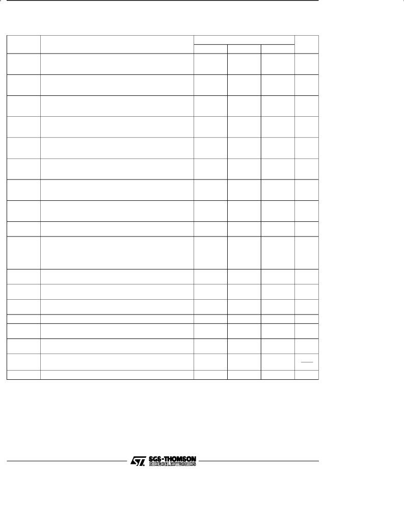
ELECTRICAL CHARACTERISTICS
VCC = ±15V, Tamb = 25oC (unless otherwise specified)
Symbol |
|
|
Parameter |
|
LM148 - LM248 - LM348 |
||
|
|
|
Min. |
Typ. |
Unit |
||
|
|
|
|
|
Max. |
||
Vio |
Input Offset Voltage (RS ≤ 10kΩ) |
|
|
|
mV |
||
|
Tamb |
= 25oC |
|
|
|
1 |
5 |
|
Tmin. |
≤ Tamb |
≤ Tmax. |
|
|
|
6 |
Iio |
Input Offset Current |
|
|
|
nA |
||
|
Tamb |
= 25oC |
|
|
|
2 |
25 |
|
Tmin. |
≤ Tamb ≤ Tmax. |
|
|
|
75 |
|
Iib |
Input Bias Current |
|
|
|
nA |
||
|
Tamb |
= 25oC |
≤ Tmax. |
|
|
30 |
100 |
|
Tmin. |
≤ Tamb |
|
|
|
300 |
|
Avd |
Large Signal Voltage Gain (Vo = ±10V, RL = 2kΩ) |
|
|
V/mV |
|||
|
Tamb |
= 25oC |
|
|
50 |
160 |
|
|
Tmin. |
≤ Tamb |
≤ Tmax. |
|
25 |
|
|
SVR |
Supply Voltage Rejection Ratio (RS ≤ 10kΩ) |
|
|
dB |
|||
|
Tamb |
= 25oC |
≤ Tmax. |
|
77 |
100 |
|
|
Tmin. |
≤ Tamb |
|
77 |
|
|
|
ICC |
Supply Current, all Amp, no Load |
|
|
|
mA |
||
|
Tamb |
= 25oC |
≤ Tmax. |
|
|
2.1 |
3.6 |
|
Tmin. |
≤ Tamb |
|
|
|
4.8 |
|
Vicm |
Input Common Mode Voltage Range |
|
|
V |
|||
|
Tamb |
= 25oC |
|
|
±12 |
|
|
|
Tmin. |
≤ Tamb |
≤ Tmax. |
|
±12 |
|
|
CMR |
Common Mode Rejection Ratio (RS ≤ 10kΩ) |
|
|
dB |
|||
|
Tamb |
= 25oC |
|
|
70 |
110 |
|
|
Tmin. |
≤ Tamb |
≤ Tmax. |
|
70 |
|
|
IOS |
Output Short-circuit Current |
|
|
|
mA |
||
|
Tamb = 25oC |
|
|
10 |
25 |
35 |
|
± Vopp |
Output Voltage Swing |
|
|
|
V |
||
|
Tamb = 25oC |
|
RL = 10kΩ |
12 |
13 |
|
|
|
|
|
|
RL = 2kΩ |
10 |
12 |
|
|
Tmin. ≤ Tamb ≤ Tmax. |
RL = 10kΩ |
12 |
|
|
||
|
|
|
|
RL = 2kΩ |
10 |
|
|
SR |
Slew Rate (VI = ±10V, RL = 10kΩ, CL = 100pF, |
0.25 |
0.5 |
V/μs |
|||
|
unity Gain) |
|
|
|
|||
tr |
Rise Time (VI = ±10V, RL = 10kΩ, CL = 100pF, |
|
|
μs |
|||
|
unity Gain) |
|
|
|
0.3 |
|
|
KOV |
Overshoot (VI = ±10V, RL = 10kΩ, CL = 100pF, |
|
5 |
% |
|||
|
unity Gain) |
|
|
|
|
||
RI |
Input Resistance |
|
0.8 |
2.5 |
MΩ |
||
GBP |
Gain Bandwidth Product (VI = 10 mV, RL = 10kΩ, |
|
|
MHz |
|||
|
CL = 100pF, f = 100kHz) |
|
0.7 |
1.3 |
|
||
THD |
Total Harmonic Distortion (f = 1kHz, Av = 20dB, |
|
|
% |
|||
|
RL = 10kΩ, CL = 100pF, Vo = 2Vpp) |
|
|
0.08 |
|
||
en |
Equivalent Input Noise Voltage |
|
|
|
nV |
||
|
(f = 1kHz, Rs = 100Ω) |
|
|
40 |
√```Hz |
||
Vo1/Vo2 |
Channel Separation |
|
|
120 |
dB |
||
3/9
 Loading...