


SGS Thomson Microelectronics LM393AD, LM393, LM293D, LM293, LM193N Datasheet
...
|
LM193 - LM293 |
|
LM393 |
|
LOW POWER DUAL VOLTAGE COMPARATORS |
.WIDE SINGLE SUPPLY VOLTAGE RANGE OR
DUAL SUPPLIES +2V TO +36V OR ±1V TO
.±18V
VERY LOW SUPPLY CURRENT (0.4mA) INDEPENDENT OF SUPPLY VOLTAGE
.(1 mW/comparator at +5V)
.LOW INPUT BIAS CURRENT : 25nA TYP
.LOW INPUT OFFSET CURRENT : ±5nA TYP
.LOW INPUT OFFSET VOLTAGE : ±1mV TYP
INPUT COMMON-MODE VOLTAGE RANGE
.INCLUDES GROUND
LOW OUTPUT SATURATION VOLTAGE :
.250mV TYP. (IO = 4mA)
DIFFERENTIAL INPUT VOLTAGE RANGE
.EQUAL TO THE SUPPLY VOLTAGE
TTL, DTL, ECL, MOS, CMOS COMPATIBLE OUTPUTS
N |
D |
DIP8 |
SO8 |
(Plastic Package) |
(Plastic Micropackage) |
P
TSSOP8
(Thin Shrink Small Outline Package)
DESCRIPTION
These devices consist of two independent low power voltage comparators designed specifically to operate from a single supply over a wide range of voltages. Operation from split power supplies is also possible.
These comparators also have a unique characteristic in that the input common-mode voltage range includesground even thoughoperatedfrom a single power supply voltage.
PIN CONNECTIONS (top view)
ORDER CODES
Part |
Temperature |
|
Package |
|
Number |
Range |
N |
D |
P |
|
|
|||
LM193 |
±55, +125oC |
• |
• |
• |
LM293 |
±40, +105oC |
• |
• |
• |
LM393 |
0, +70oC |
• |
• |
• |
Example : LM393D
1 |
|
|
8 |
1 |
- Output 1 |
|
|
|
|
|
2 |
- Inverting input 1 |
|
2 |
- |
|
7 |
3 |
- Non-inverting input 1 |
|
|
4 |
- |
||||
|
|
|
|
- VCC |
||
3 |
+ |
- |
6 |
5 |
- Non-inverting input 2 |
|
6 |
- Inverting input 2 |
|||||
|
|
|
|
|||
4 |
|
+ |
5 |
7 |
- Output 2 |
|
|
8 |
+ |
||||
|
|
|
|
- VCC |
June 1998 |
1/10 |

LM193 - LM293 - LM393
SCHEMATIC DIAGRAM (1/2 LM193)
VCC
μ |
μ |
μ |
μ |
3.5 A |
100 A |
3.5 A |
100 A |
Non-inverting
Input
VCC |
VO |
VCC |
Inverting
Input
VCC
ABSOLUTE MAXIMUM RATINGS
Symbol |
Parameter |
LM193 |
LM293 |
LM393 |
Unit |
VCC |
Supply Voltage |
±18 or 36 |
±18 or 36 |
±18 or 36 |
V |
Vid |
Differential Input Voltage |
±36 |
±36 |
±36 |
V |
Vi |
Input Voltage |
±0.3 to +36 |
±0.3 to +36 |
±0.3 to +36 |
V |
|
Output Short-circuit to Ground ± (note 1) |
|
Infinite |
|
|
Ptot |
Power Dissipation |
|
830 |
|
mW |
Toper |
Operating Free-air TemperatureRange |
±55 to +125 |
±40 to +105 |
0 to +70 |
oC |
Tstg |
Storage Temperature Range |
±65 to +150 |
±65 to +150 |
±65 to +150 |
oC |
Notes : 1. Short-ci rcuit from the output to VC C+ can cause excessi ve heat ing and eventual destruction. T he maximum output current is approxi mately 20mA, independent of the magnitude of VCC+.
2/10
LM193 - LM293 - LM393
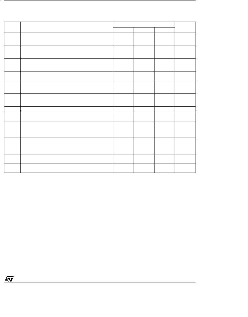
ELECTRICAL CHARACTERISTICS
VCC+ = +5V, VCC± = 0V, Tamb = 25oC (unless otherwise specified)
Symbol |
|
Parameter |
LM193 - LM293 - LM393 |
|
Unit |
||
|
Min. |
Typ. |
Max. |
||||
|
|
|
|
||||
Vio |
Input Offset Voltage ± (note 2) |
|
|
|
|
mV |
|
|
Tamb = |
+25oC |
|
1 |
5 |
|
|
|
Tmin. ≤ |
Tamb ≤ Tmax. |
|
|
9 |
|
|
Iib |
Input Bias Current ± (note 3) |
|
|
|
|
nA |
|
|
Tamb = |
+25oC |
|
25 |
250 |
|
|
|
Tmin. ≤ Tamb ≤ Tmax. |
|
|
400 |
|
||
Iio |
Input Offset Current |
|
|
|
|
nA |
|
|
Tamb = |
+25oC |
|
5 |
50 |
|
|
|
Tmin. ≤ |
Tamb ≤ Tmax. |
|
|
150 |
|
|
Avd |
Large Signal Voltage Gain |
|
|
|
|
V/mV |
|
|
VCC = 15V, RL = 15kΩ, Vo = 1 to 11V |
50 |
200 |
|
|
|
|
ICC |
Supply Current (all comparators) |
|
0.4 |
1 |
|
mA |
|
|
VCC = |
5V, no load |
|
|
|
||
|
VCC = 30V, no load |
|
1 |
2.5 |
|
||
Vicm |
Input Common Mode Voltage Range - (note 4) |
|
|
VCC+ -1.5 |
V |
||
|
Tamb = |
+25oC |
0 |
|
|
||
|
Tmin. ≤ |
Tamb ≤ Tmax. |
0 |
|
VCC+ |
-2 |
|
Vid |
Differential Input Voltage - (note 6) |
|
|
VCC |
+ |
V |
|
|
|
|
|||||
Isink |
Output Sink Current |
|
|
|
|
mA |
|
|
(Vid = -1V, VO = 1.5V) |
6 |
16 |
|
|
|
|
VOL |
Low Level Output Voltage |
|
|
|
|
mV |
|
|
(Vid = -1V, Isink = 4mA) |
|
|
|
|
|
|
|
Tamb = |
25oC |
|
250 |
400 |
|
|
|
Tmin. ≤ |
Tamb ≤ Tmax |
|
|
700 |
|
|
IOH |
High Level Output Current |
|
|
|
|
|
|
|
(Vid = 1V, VCC = VO = 30V) |
|
|
|
|
|
|
|
Tamb = |
25oC |
|
0.1 |
|
|
nA |
|
Tmin. ≤ |
Tamb ≤ Tmax |
|
|
1 |
|
μA |
tre |
Response Time |
|
|
|
|
μs |
|
|
(RL = 5.1kΩ to VCC+) ± (note 5) |
|
1.3 |
|
|
|
|
trel |
Large Signal Response Time |
|
|
|
|
ns |
|
|
(Vi = TTL, Vref = +1.4 V, RL = 5.1kΩ to VCC+) |
|
300 |
|
|
|
|
No tes : |
2. At out put switch point, VO ≈ 1.4V, RS = 0Ω with VC C+ from 5V to 30V and over the full input common-mode range |
||||||
|
(0V to VCC+ 1.5V). |
|
|
|
|
|
|
3.The direct ion of the input current is out of the IC due to the PNP i nput stage. T his current is essent ial ly const ant, independent of the state of the output, so no loadi ng charge exists on the reference or input l ines.
4. |
The input common-mode volt age of either input signal vol tage shoul d not be all owed to go negat ive by more than |
|
0.3V . |
|
The upper end of the common-mode vol tage range is VC C+ ±1.5V , but either or bot h inputs can go to +30V wi thout |
|
damage. |
5. |
The response ti me specifi ed is for a 100mV i nput step wit h 5mV overdrive. For l arger overdrive signal s 300ns |
|
can be obtained. |
6. |
Posit ive excursions of i nput voltage may exceed the power suppl y level. A s l ong as the other voltage remai ns |
|
within the common-mode range the comparator wil l provide a proper output state. The low input voltage state must |
|
not be less than ±0.3V (or 0.3V below the negat ive power supply, if used). |
3/10
 Loading...