


SGS Thomson Microelectronics LM339D, LM339AN, LM339AD, LM339, LM339N Datasheet
...
|
LM139,A |
|
LM239,A-LM339,A |
|
LOW POWER QUAD VOLTAGE COMPARATORS |
.WIDE SINGLE SUPPLY VOLTAGE RANGE OR DUAL SUPPLIES FOR ALL DEVICES : +2V TO
.+36V OR ±1V TO ±18V
VERY LOW SUPPLY CURRENT (1.1mA) INDEPENDENT OF SUPPLY VOLTAGE
.(1.4mW/comparator at +5V)
.LOW INPUT BIAS CURRENT : 25nA TYP
.LOW INPUT OFFSET CURRENT : ±5nA TYP
.LOW INPUT OFFSET VOLTAGE : ±1mV TYP
INPUT COMMON-MODE VOLTAGE RANGE
.INCLUDES GROUND
LOW OUTPUT SATURATION VOLTAGE :
.250mV TYP. (IO = 4mA)
DIFFERENTIAL INPUT VOLTAGE RANGE
.EQUAL TO THE SUPPLY VOLTAGE
TTL, DTL, ECL, MOS, CMOS COMPATIBLE OUTPUTS
DESCRIPTION
Thesedevices consist of fourindependentprecision voltage comparators with an offset voltage specifications as low as 2mV max for LM339A, LM239A and LM139A. All these comparators were designed specifically to operate from a single power supply over a wide range of voltages. Operation from split power supplies is also possible.
These comparators also have a unique characteristic in that the input common-mode voltage range includesground even thoughoperatedfrom a single power supply voltage.
PIN CONNECTIONS (top view)
Output 2 |
1 |
Output 1 |
2 |
V + |
3 |
CC |
|
Invertinginput 1 |
4 |
Non-inverting input 1 |
5 |
Invertinginput 2 |
6 |
Non-inverting input 2 |
7 |
N |
D |
DIP14 |
SO14 |
(Plastic Package) |
(Plastic Micropackage) |
P
TSSOP14
(Thin Shrink Small Outline Package)
ORDER CODES
Part |
Temperature |
Package |
||
Number |
Range |
N |
D |
P |
|
|
|||
LM139,A |
-55, +125oC |
• |
• |
• |
LM239,A |
-40, +105oC |
• |
• |
• |
LM339,A |
0, +70oC |
• |
• |
• |
Example : LM139AN
14 |
Output 3 |
13 |
Output 4 |
12 |
VCC- |
11 |
Non-invertinginput 4 |
10 |
Inverting input 4 |
9 |
Non-invertinginput 3 |
8 |
Inverting input 3 |
June 1998 |
1/10 |

LM139,A - LM239,A - LM339,A
SCHEMATIC DIAGRAM (1/4 LM139)
VCC
μ |
μ |
μ |
μ |
3.5 A |
100 A |
3.5 A |
100 A |
Non-inverting
Input
VO
Inverting
Input
VCC
ABSOLUTE MAXIMUM RATINGS
Symbol |
Parameter |
LM139,A |
LM339,A |
Unit |
|
LM239,A |
|||||
|
|
|
|
||
VCC |
Supply Voltage |
±18 to 36 |
±18 to 36 |
V |
|
Vid |
Differential Input Voltage |
±36 |
±36 |
V |
|
VI |
Input Voltage |
-0.3 to +36 |
-0.3 to +36 |
V |
|
|
Output Short-circuit to Ground - (note 1) |
Infinite |
|
||
Ptot |
Power Dissipation |
570 |
570 |
mW |
|
Toper |
Operating Free-air Temperature Range |
-55, +125 |
0, +70 |
oC |
|
|
LM239,A |
-40, +105 |
|
|
|
Tstg |
Storage Temperature Range |
-65, +150 |
-65, +150 |
oC |
|
Notes : 1. S hort-circui t f rom t he output t o VC C+ can cause excessive heat i ng and eventual dest ruct i on. T he maxi mum output current is approxi mat el y 20mA, i ndependent of t he magni tude of VCC + .
2/10
LM139,A - LM239,A - LM339,A
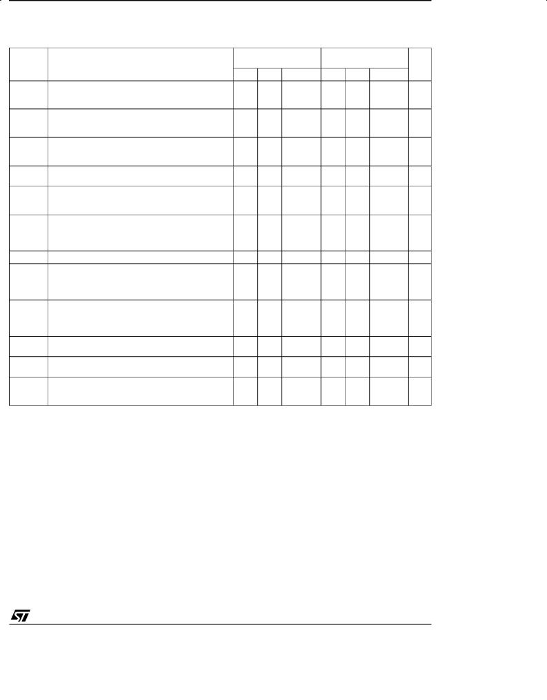
ELECTRICAL CHARACTERISTICS
VCC+ = +5V, VCC- = GND, Tamb = 25oC (unless otherwise specified)
|
|
LM139A - LM239A |
LM139 - LM239 |
||||
Symbol |
Parameter |
|
LM339A |
|
LM339 |
||
|
|
Min. |
Typ. |
Max. |
Min. |
Typ. |
Max. |
Vio |
Input Offset Voltage ± (note 2) |
|
|
|
|
|
|
|
Tamb = +25oC |
|
1 |
2 |
|
1 |
5 |
|
Tmin. ≤ Tamb ≤ Tmax. |
|
|
4 |
|
|
9 |
Iio |
Input Offset Current |
|
|
|
|
|
|
|
Tamb = +25oC |
|
3 |
25 |
|
5 |
50 |
|
Tmin. ≤ Tamb ≤ Tmax. |
|
|
100 |
|
|
150 |
Iib |
Input Bias Current (II+ or II±) - (note 3) |
|
|
|
|
|
|
|
Tamb = +25oC |
|
25 |
100 |
|
25 |
250 |
|
Tmin. ≤ Tamb ≤ Tmax. |
|
|
300 |
|
|
400 |
Avd |
Large Signal Voltage Gain |
|
|
|
|
|
|
|
(VCC = 15V, RL =15kΩ, VO = 1 to 11V) |
50 |
200 |
|
50 |
200 |
|
ICC |
Supply Current (all comparators) |
|
1.1 |
2 |
|
1.1 |
2 |
|
VCC = +5V, no load |
|
|
||||
|
VCC = +30V, no load |
|
1.3 |
2.5 |
|
1.3 |
2.5 |
Vicm Input Common Mode Voltage Range - (note 4) |
|
|
|
|
|
|
|
|
(VCC = 30V) |
|
|
VCC+-1.5 |
|
|
VCC+-1.5 |
|
Tamb = +25oC |
0 |
|
0 |
|
||
|
Tmin. ≤ Tamb ≤ Tmax. |
0 |
|
VCC+ -2 |
0 |
|
VCC+ -2 |
Vid |
Differential Input Voltage - (note 6) |
|
|
+ |
|
|
+ |
|
|
VCC |
|
|
VCC |
||
VOL |
Low Level Output Voltage |
|
|
|
|
|
|
|
(Vid = -1V, Isink = 4mA) |
|
|
|
|
|
|
|
Tamb = +25oC |
|
250 |
400 |
|
250 |
400 |
|
Tmin. ≤ Tamb ≤ Tmax. |
|
|
700 |
|
|
700 |
IOH |
High Level Output Current ( Vid = 1V) |
|
|
|
|
|
|
|
(VCC = VO = 30V) |
|
|
|
|
|
|
|
Tamb = +25oC |
|
0.1 |
|
|
0.1 |
|
|
Tmin. ≤ Tamb ≤ Tmax. |
|
|
1 |
|
|
1 |
Isink |
Output Sink Current |
|
|
|
|
|
|
|
(Vid = -1V, VO = 1.5V) |
6 |
16 |
|
6 |
16 |
|
tre |
Response Time ± (note 5) |
|
|
|
|
|
|
|
(RL = 5.1kΩ connected to VCC+) |
|
1.3 |
|
|
1.3 |
|
trel |
Large Signal Response Time |
|
|
|
|
|
|
|
(RL = 5.1kΩ connected to VCC+, eI = TTL, |
|
|
|
|
|
|
|
V(ref) = +1.4V) |
|
300 |
|
|
300 |
|
Unit
mV
nA
nA
V/mV
mA
V
V mV
nA
μA
mA
μs
ns
Notes : 2. |
A t out put swit ch poi nt, VO ≈ 1. 4V , RS = 0 wi th VC C+ from 5V t o 30V, and over the full i nput common-mode range |
|
(0V t o V C C+ ±1.5V). |
3. |
The di rect ion of the i nput current i s out of t he IC due t o t he P NP i nput stage. This current is essent i al ly con- |
|
stant , i ndependent of the st ate of t he out put , so no loading charge exi st s on t he reference of input l ines. |
4. |
The i nput common-mode vol t age of ei ther input si gnal volt age should not be al lowed t o go negati ve by more |
|
than 0.3V. T he upper end of the common-mode volt age range i s VC C+ ±1. 5V, but ei ther or both i nput s can go |
|
to +30V wi thout damage. |
5. |
The response t ime speci fi ed i s f or a 100mV input st ep wi th 5mV overdri ve. For larger overdri ve signal s 300ns |
|
can be obt ained. |
6.P osi t i ve excursi ons of i nput vol tage may exceed the power suppl y level . As long as the ot her vol t age remai ns wi t hi n the common-mode range, the comparat or wi ll provide a proper output st at e. T he low input vol tage stat e must not be l ess than ±0.3V (or 0.3V bel low t he negat ive power supply, i f used).
3/10
 Loading...