


SGS Thomson Microelectronics LM317P, LM317K, LM317D2T, LM217T, LM217K Datasheet
...
|
LM117/217 |
|
LM317 |
1.2V TO 37V VOLTAGE REGULATOR
■OUTPUT VOLTAGE RANGE : 1.2 TO 37V
■OUTPUT CURRENT IN EXCESS OF 1.5A
■0.1% LINE AND LOAD REGULATION
■FLOATING OPERATION FOR HIGH VOLTAGES
■COMPLETE SERIES OF PROTECTIONS : CURRENT LIMITING, THERMAL SHUTDOWN AND SOA CONTROL
DESCRIPTION |
|
|
|
|
The LM117/LM217/LM317 |
are monolithic |
|
|
D2PAK |
integrated circuit in TO-220, ISOWATT220, TO-3 |
TO-3 |
|
||
and D2PAK packages intended for use as |
|
|
|
|
positive adjustable voltage regulators. |
|
|
|
|
They are designed to supply more than 1.5A of |
|
|
|
|
load current with an output voltage adjustable |
|
|
|
|
over a 1.2 to 37V range. |
|
|
|
|
The nominal output voltage is selected by means |
|
|
|
|
of only a resistive divider, making the device |
|
|
|
|
exceptionally easy to use and eliminating the |
|
|
|
|
stocking of many fixed regulators. |
|
|
|
|
|
|
TO-220 |
ISOWATT220 |
|
ABSOLUTE MAXIMUM RATING |
|
|
|
|
Symbol |
Parameter |
|
Value |
Unit |
Vi-o
IO
Top
Ptot
Tst g
Input-output Differential Voltage |
|
40 |
V |
Output Current |
Intenrally Limited |
|
|
Operating Junction Temperature for: LM117 |
-55 |
to 150 |
oC |
LM217 |
-25 |
to 150 |
oC |
LM317 |
0 to 125 |
oC |
|
Power Dissipation |
Internally Limited |
|
|
Storage Temperature |
- 65 to 150 |
oC |
|
THERMAL DATA
Symbol |
Parameter |
|
TO-3 |
TO-220 |
ISOWATT220 |
D2PAK |
Unit |
Rthjca se |
Thermal Resistance Junction-case |
Max |
4 |
3 |
4 |
3 |
oC/W |
Rthjamb |
Thermal Resistance Junction-ambient |
Max |
35 |
50 |
60 |
62.5 |
oC/W |
November 1999 |
1/11 |

LM117/217/317
CONNECTION DIAGRAM AND ORDERING NUMBERS (top view)
TO-220 |
ISOWATT220 |
D2PAK |
TO-3 |
Type |
TO-3 |
TO-220 |
ISOWATT220 |
D2PAK |
LM117 |
LM117K |
|
|
|
LM217 |
LM217K |
LM217T |
|
LM217D2T |
LM317 |
LM317K |
LM317T |
LM317P |
LM317D2T |
SCHEMATIC DIAGRAM
2/11
LM117/217/317
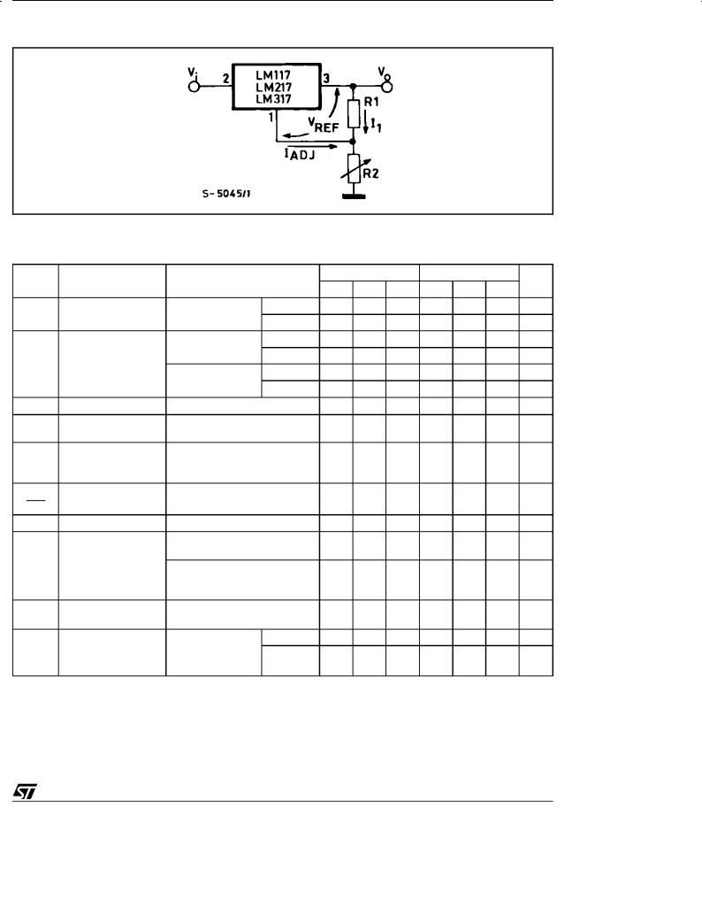
BASIC ADJUSTABLE REGULATOR
ELECTRICAL CHARACTERISTICS (Vi - Vo = 5 V, Io = 500 mA, IMAX = 1.5A and PMAX = 20W, unless otherwise specified)
Symbol |
Parameter |
Test Conditions |
LM117/LM217 |
LM317 |
Unit |
|
|
|
Min. Typ. Max. Min. Typ. Max. |
|
|
Vo |
Line Regulation |
Vi - Vo = 3 to 40 V |
Vo |
Load Regulation |
Vo ≤ 5V |
|
|
Io = 10 mA to IMAX |
|
|
Vo ≥ 5V |
|
|
Io = 10 mA to IMAX |
IADJ |
Adjustment Pin Current |
|
IADJ |
Adjustment Pin Current |
Vi - Vo = 2.5 to 40 V |
|
|
Io = 10 mA to IMAX |
VREF |
Reference Voltage |
Vi - Vo = 2.5 to 40 V |
|
(between pin 3 and pin |
Io = 10 mA to IMAX |
|
1) |
PD ≤ PMAX |
Vo |
Output Voltage |
|
Vo |
Temperature Stability |
|
Tj = 25 oC |
0.01 |
0.02 |
|
0.01 0.04 %/V |
||
|
0.02 |
0.05 |
|
0.02 |
0.07 |
%/V |
Tj = 25 oC |
5 |
15 |
|
5 |
25 |
mV |
|
20 |
50 |
|
20 |
70 |
mV |
Tj = 25 oC |
0.1 |
0.3 |
|
0.1 |
0.5 |
% |
|
0.3 |
1 |
|
0.3 |
1.5 |
% |
|
50 |
100 |
|
50 |
100 |
μA |
|
0.2 |
5 |
|
0.2 |
5 |
μA |
1.2 |
1.25 |
1.3 |
1.2 |
1.25 |
1.3 |
V |
|
1 |
|
|
1 |
|
% |
Io (m in) |
Minimum Load Current |
Vi - Vo = 40 V |
|
|
3.5 |
5 |
|
3.5 |
10 mA |
Io (max ) |
Maximum Load |
Vi - Vo ≤ 15 V |
|
1.5 |
2.2 |
|
1.5 |
2.2 |
A |
|
Current |
PD < PMAX |
|
|
|
|
|
|
|
|
|
Vi - Vo = 40 V |
|
|
0.4 |
|
|
0.4 |
A |
|
|
PD < PMAX |
|
|
|
|
|
|
|
|
|
Tj = 25 oC |
|
|
|
|
|
|
|
eN |
Output Noise Voltage |
B = 10Hz to 10KHz |
|
|
0.003 |
|
|
0.003 |
% |
|
(percentance of VO) |
Tj = 25 oC |
|
|
|
|
|
|
|
SVR |
Supply Voltage |
Tj = 25 oC |
CADJ =0 |
|
65 |
|
|
65 |
dB |
|
Rejection (*) |
f = 120 Hz |
CADJ=10μF |
66 |
80 |
|
66 |
80 |
dB |
|
|
|
|
(*) CADJ is connected between pin 1 and ground.
Note:
(1) Unless otherwise specified the above specs, apply over the following conditions : LM 117 Tj = ± 55 to 150°C; LM 217 Tj = ± 25 to 150°C ; LM 317 Tj = 0 to 125°C.
3/11
LM117/217/317
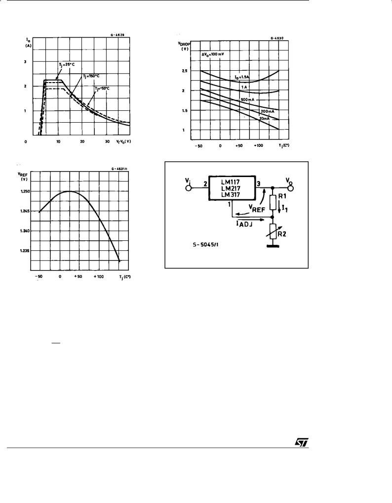
Figure 1 : Output Current vs. Input-output Differential Voltage.
Figure 3 : Reference Voltage vs. Junction
APPLICATION INFORMATION
The LM117/217/317 provides an internal reference voltage of 1.25V between the output and adjustments terminals. This is used to set a constant current flow across an external resistor divider (see fig. 4), giving an output voltage VO of:
VO = VREF (1 + R2) + IADJ R2
R1
The device was designed to minimize the term IADJ (100μA max) and to maintain it very constant with line and load changes. Usually, the error term IADJ R2 can be neglected. To obtain the previous requirement, all the regulator quiescent current is returned to the output terminal, imposing a minimum load current condition. If the load is insufficient, the output voltage will rise.
Since the LM117/217317 is a floating regulator and ºseesº only the input-to-output differential
Figure 2 : Dropout Voltage vs. Junction Temperature.
Figure 4 : Basic Adjustable Regulator.
voltage, supplies of very high voltage with respect to ground can be regulated as long as the maximum input-to-output differential is not exceeded. Furthermore, programmable regulator are easily obtainable and, by connecting a fixed resistor between the adjustment and output, the device can be used as a precision current regulator.
In order to optimise the load regulation, the current set resistor R1 (see fig. 4) should be tied as close as possible to the regulator, while the ground terminal of R2 should be near the ground of the load to provide remote ground sensing.
Performance may be improved with added capacitance as follow:
An input bypass capacitor of 0.1μF
An adjustment terminal to ground 10μF capacitor
4/11
 Loading...