


SGS Thomson Microelectronics LM324AN, LM324A, LM324D, LM224D, LM224N Datasheet
...LM124A
LM224A - LM324A
LOW POWER QUAD OPERATIONAL AMPLIFIERS
.
.WIDE GAIN BANDWIDTH / 1.3MHz
.LARGE VOLTAGE GAIN : 100dB
VERY LOW SUPPLY CURRENT/AMPLI :
.375μA
.LOW INPUT BIAS CURRENT : 20nA
.LOW INPUT OFFSET VOLTAGE : 3mV max.
.LOW INPUT OFFSET CURRENT : 2nA WIDE POWER SUPPLY RANGE : SINGLE SUPPLY : +3V TO +30V
.DUAL SUPPLIES : ±1.5V TO ±15V
INPUT COMMON-MODE VOLTAGE RANGE
.INCLUDES GROUND
ESD INTERNAL PROTECTION : 2kV
DESCRIPTION
These circuits consist of four independent, high gain, internally frequencycompensated operational amplifiers. They operate from a single power supply over a wide range of voltages. Operation from split power supplies is also possible and the low power supply current drain is independent of the magnitude of the power supply voltage.
All the pins are protected against electrostatic discharges up to 2000V (as a consequence, the input
voltages must not exceed the magnitude of VCC+ or VCC-.)
PIN CONNECTIONS (top view)
Output 1 |
1 |
|
Inve rting Input 1 |
2 |
- |
Non-inve rting Input 1 |
3 |
+ |
|
||
VCC + |
4 |
|
Non-inve rting Input 2 |
5 |
+ |
Inve rting Input 2 |
6 |
- |
|
||
Output 2 |
7 |
|
N |
D |
DIP14 |
SO14 |
(Plastic Package) |
(Plastic Micropackage) |
ORDER CODES
Part |
Temperature |
Number |
Range |
LM124A |
-55oC, +125oC |
LM224A |
-40oC, +105oC |
LM324A |
0oC, +70oC |
Example : LM224AN
14 Output 4
-13 Inve rting Input 4
+12 Non-inve rting Input 4 11 VCC -
+10 Non-inve rting Input 3
-9 Inve rting Input 3
8 Output 3
Package
ND
••
••
••
November 1997 |
1/13 |

LM124A - LM224A - LM324A
SCHEMATIC DIAGRAM (1/4 LM124A)
VCC
|
|
6 |
μA |
4μA |
100μA |
|
|
|
|
||
|
|
|
|
C C |
Q5 |
|
|
|
|
Q6 |
|
|
|
|
|
|
|
Inve rting |
Q2 |
Q3 |
|
Q7 |
|
|
|
|
|
||
input |
Q1 |
|
|
Q4 |
|
|
|
|
|||
|
|
|
|
|
R S C |
Non-inve rting |
|
|
|
|
Q11 |
input |
|
|
|
|
Output |
|
|
|
|
|
|
|
|
|
|
|
Q13 |
|
|
|
|
Q10 |
Q12 |
|
Q8 |
Q9 |
|
50μA |
|
|
|
|
|
|
|
GND
ABSOLUTE MAXIMUM RATINGS
Symbol |
Parameter |
|
LM124A |
LM224A |
LM324A |
Unit |
Vcc |
Supply Voltage |
|
|
±16 or 32 |
|
V |
Vi |
Input Voltage |
|
|
-0.3 to +32 |
|
V |
Vid |
Differential Input Voltage - (*) |
|
+32 |
+32 |
+32 |
V |
Ptot |
Power Dissipation |
N Suffix |
500 |
500 |
500 |
mW |
|
|
D Suffix |
- |
400 |
400 |
mW |
- |
Output Short-circuit Duration - (note 1) |
|
Infinite |
|
|
|
Iin |
Input Current ± (note 6) |
|
50 |
50 |
50 |
mA |
Toper |
Operating Free Air Temperature Range |
-55 to +125 |
-40 to +105 |
0 to +70 |
oC |
|
Tstg |
Storage Temperature Range |
|
-65 to +150 |
-65 to +150 |
-65 to +150 |
oC |
(* ) - Ei ther or bo th i nput vo ltages mu st not exceed the magn itude of VCC+ o r VCC - .
2/13

LM124A - LM224A - LM324A
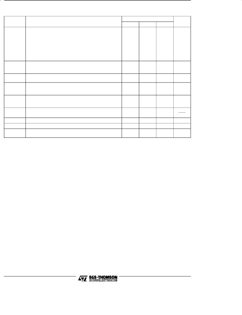
ELECTRICAL CHARACTERISTICS
VCC+ = +5V, VCC± = Ground, VO = 1.4V, Tamb = +25oC (unless otherwise specified)
Symbol |
Parameter |
LM124A - LM224A - LM324A |
|||
Min. |
Typ. |
Unit |
|||
|
|
|
Max. |
||
Vio |
Input Offset Voltage (note 3) |
|
|
|
mV |
|
Tamb = +25oC |
|
|
2 |
3 |
|
Tmin. ≤ Tamb ≤ Tmax. |
|
|
|
5 |
Iio |
Input Offset Current |
|
|
|
nA |
|
Tamb = +25oC |
|
|
2 |
20 |
|
Tmin. ≤ Tamb ≤ Tmax. |
|
|
|
40 |
Iib |
Input Bias Current (note 2) |
|
|
|
nA |
|
Tamb = +25oC |
|
|
20 |
100 |
|
Tmin. ≤ Tamb ≤ Tmax. |
|
|
|
200 |
Avd |
Large Signal Voltage Gain |
|
|
|
V/mV |
|
(VCC+ = +15V, RL = 2kΩ, VO = 1.4V to 11.4V) |
|
|
|
|
|
Tamb = +25oC |
|
50 |
100 |
|
|
Tmin. ≤ Tamb ≤ Tmax. |
|
25 |
|
|
SVR |
Supply Voltage Rejection Ratio (RS ≤ 10kΩ) |
|
|
dB |
|
|
(VCC+ = 5V to 30V) |
|
|
|
|
|
Tamb = +25oC |
|
65 |
110 |
|
|
Tmin. ≤ Tamb ≤ Tmax. |
|
65 |
|
|
ICC |
Supply Current, all Amp, no load |
|
|
mA |
|
|
Tamb = +25oC |
VCC = +5V |
|
0.7 |
1.2 |
|
Tmin. ≤ Tamb ≤ Tmax. |
VCC = +30V |
|
1.5 |
3 |
|
VCC = +5V |
|
0.8 |
1.2 |
|
|
|
VCC = +30V |
|
1.5 |
3 |
Vicm |
Input Common Mode Voltage Range |
|
|
V |
|
|
(VCC = +30V) - (note 4) |
|
|
|
|
|
Tamb = +25oC |
|
0 |
|
VCC -1.5 |
|
Tmin. ≤ Tamb ≤ Tmax. |
|
0 |
|
VCC -2 |
CMR |
Common-mode Rejection Ratio (RS ≤ 10kΩ) |
|
|
dB |
|
|
Tamb = +25oC |
|
70 |
80 |
|
|
Tmin. ≤ Tamb ≤ Tmax |
|
60 |
|
|
Isource |
Output Current Source (Vid = +1V) |
|
|
mA |
|
|
VCC = +15V, Vo = +2V |
|
20 |
40 |
70 |
Isink |
Output Sink Current (Vid = -1V) |
10 |
20 |
mA |
|
|
VCC = +15V, Vo = +2V |
|
|||
|
VCC = +15V, Vo = +0.2V |
|
12 |
50 |
μA |
3/13
LM124A - LM224A - LM324A
ELECTRICAL CHARACTERISTICS (continued)
Symbol |
|
Parameter |
LM124A - LM224A - LM324A |
Unit |
||
|
Min. |
Typ. |
Max. |
|||
|
|
|
|
|||
VOH |
High Level Output Voltage |
|
|
|
V |
|
|
(VCC = +30V) |
RL = 2kΩ |
|
|
|
|
|
Tamb = +25oC |
26 |
27 |
|
|
|
|
Tmin. ≤ Tamb ≤ |
Tmax. |
26 |
|
|
|
|
Tamb = +25oC |
RL = 10kΩ |
27 |
28 |
|
|
|
Tmin. ≤ Tamb ≤ |
Tmax. |
27 |
|
|
|
|
(VCC = +5V, RL = 2kΩ) |
|
|
|
|
|
|
Tamb = +25oC |
|
3.5 |
|
|
|
|
Tmin. ≤ Tamb ≤ Tmax. |
3 |
|
|
|
|
VOL |
Low Level Output Voltage (RL = 10kΩ) |
|
|
|
mV |
|
|
Tamb = +25oC |
|
|
5 |
20 |
|
|
Tmin. ≤ Tamb ≤ Tmax. |
|
|
20 |
|
|
SR |
Slew Rate (VCC = 15V, VI = 0.5 to 3V, |
|
|
|
V/μs |
|
|
RL = 2kΩ, CL = 100pF, unity gain) |
|
0.4 |
|
|
|
GBP |
Gain Bandwidth Product (VCC = 30V |
|
|
|
MHz |
|
|
f = 100kHz, Vin = 10mV |
|
|
|
|
|
|
RL = 2kΩ, CL = 100pF) |
|
1.3 |
|
|
|
THD |
Total Harmonic Distortion |
|
|
|
% |
|
|
(f = 1kHz, AV = 20dB, RL = 2kΩ, VO = 2Vpp |
|
|
|
|
|
|
CL = 100pF, VCC = 30V) |
|
0.015 |
|
|
|
en |
Equivalent Input Noise Voltage |
|
|
|
nV |
|
|
(f = 1kHz, Rs = 100Ω, VCC = 30V) |
|
40 |
|
√```Hz |
|
DVio |
Input Offset Voltage Drift |
|
7 |
30 |
μV/oC |
|
DIIO |
Input Offset Current Drift |
|
10 |
200 |
pA/oC |
|
VO1/VO2 |
Channel Separation (note 5) |
|
|
|
dB |
|
|
1kHz ≤ f ≤ 20kHz |
|
|
120 |
|
|
Notes : 1. Short -circui t s f rom t he out put t o VC C can cause excessi ve heat i ng if VC C > 15V. T he maxi mum out put current is approxi mat el y 40mA i ndependent of the magni t ude of VC C. Destructi ve di ssipat i on can res ult f rom simul taneous short -circuit on al l ampli f iers.
2.The di rect ion of the i nput current is out of t he IC. Thi s current is essenti al l y constant, i ndependent of the st ate of the out put so no l oadi ng change exists on the i nput l i nes.
3.Vo = 1. 4V , Rs = 0Ω, 5V < V CC + < 30V , 0 < Vic < V C C+ - 1.5V
4.The i nput common-mode vol t age of eit her i nput si gnal volt age shoul d not be allowed to go negat i ve by more than 0.3V . T he upper end of the common-mode vol tage range i s VC C+ - 1.5V , but eit her or bot h i nput s can go
to +32V wi thout damage.
5. Due t o the proxi mit y of ex ternal component s insure t hat coupl ing i s not ori gi nat ing vi a stray capaci t ance between these ext ernal part s. T hi s t ypi call y can be detect ed as t his t ype of capaci tance i ncreases at higher f requences.
6. This input current onl y exi sts when t he volt age at any of t he i nput leads is driven negat ive. It i s due t o t he coll ect or-base juncti on of t he i nput PNP transistor becomi ng forward biased and thereby act ing as input diodes clamps. I n addit i on to thi s di ode act i on, there i s al so NPN parasit i c act ion on the I C chip. t hi s t ransi st or acti on can cause t he output vol t ages of the Op-amps t o go t o the VCC volt age l evel (or to ground f or a l arge overdri ve) f or t he ti me durat ion t han an input i s driven negati ve.
This i s not destruct i ve and normal out put wi l l set up again f or i nput vol tage higher t han -0.3V.
4/13
 Loading...