


SGS Thomson Microelectronics LM2931D, LM2931AV50, LM2931AV33, LM2931BZ50, LM2931BZ33 Datasheet
...
|
LM2931 |
|
SERIES |
|
VERY LOW DROP VOLTAGE |
|
REGULATOR WITH INHIBIT FUNCTION |
■VERY LOW DROPOUT VOLTAGE (0.15V TYP. AT 10mA LOAD)
■LOW QUIESCENT CURRENT (TYP 2.5mA, AT 100mA LOAD)
■OUTPUT CURRENT UP TO 100mA
■ADJUSTABLE (FROM VOUT=2.5V ONLY SO-8) AND FIXED (3.3V & 5V) OUTPUT VOLTAGE VERSION
■INTERNAL CURRENT AND THERMAL LIMIT
■LOAD DUMP PROTECTION UP TO 60V
■REVERSE TRANSIENT PROTECTION UP TO -50V
■TEMPERATURE RANGE: -40 TO 125 oC
■PACKAGE AVAILABLE: TO-92, DPAK, TO-220, SO-8 (WITH INHIBIT CONTROL)
DESCRIPTION
The LM2931 series are very low drop regulators. The very low drop voltage and the low quiescent current make them particular suitable for low noise, low power applications and in battery powered systems. In the 8 pin configation (SO-8), fully compatible to the older L78L00 family, a shut down Logic Control function is available.
This means that when the device is used as a
SO-8
TO-92
TO-252 (DPAK) |
TO-220 |
local regulator is possible to put a part of the board in stand-by decreasing the total power consumption. Ideal for automotive application the LM2931 is proteceted from reverse battery installations or 2 battery jumps. During the transient, suchs as a a load dump (60V) when the input voltage can exceed the specified maximum operating input voltage (26V), the regulator will automatically shut down to protect both internal circuit and the load.
BLOCK DIAGRAM
December 1999 |
1/16 |
LM2931 SERIES
ABSOLUTE MAXIMUM RATINGS
Symbol |
Parameter |
Value |
Unit |
|
VIN |
DC Positive Input Voltage |
|
40 |
V |
VIN |
DC Reverse Input Voltage |
|
-15 |
V |
VIN |
Transient Input Voltage (τ < 100ms) |
|
60 |
V |
VIN |
Transient Reverse Input Voltage (τ < 100ms) |
|
-50 |
V |
VI NH |
Inhibit Input Voltage |
|
40 |
V |
IOUT |
Output Current |
Internally Limited |
mA |
|
Tstg |
Storage Temperature Range |
-65 |
to 150 |
o C |
To p |
Operating Junction Temperature Range |
-40 |
to 125 |
o C |
Absolute Maximum Ratings are those value beyond which damage to the device may occur. Functional operation under these condition is not implied.
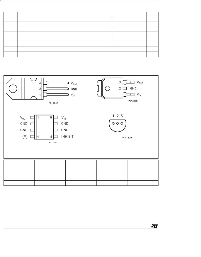
CONNECTION DIAGRAM AND ORDERING NUMBERS (top view)
TO-220 |
DPAK |
BOTTOM VIEW
|
|
|
pin 1 |
= OUT |
|
|
|
|
pin 2 |
= GND |
|
(*) = N.C. for FIXED and ADJ for ADJUSTABLE |
|
pin 3 |
= IN |
|
|
|
SO-8 |
|
|
TO-92 |
|
TO-220 |
DPAK (*) |
TO-92 (*) |
|
SO-8 (*) |
Output Voltage |
LM2931AV33 |
LM2931ADT33 |
LM2931AZ33 |
LM2931AD33 |
3.3V |
|
LM2931BV33 |
LM2931BDT33 |
LM2931BZ33 |
LM2931BD33 |
3.3V |
|
LM2931AV50 |
LM2931ADT50 |
LM2931AZ50 |
LM2931AD50 |
5V |
|
LM2931BV50 |
LM2931BDT50 |
LM2931BZ50 |
LM2931BD50 |
5V |
|
|
|
|
LM2931D |
2.5V to 26V |
|
(*) Available in Tape & Reel with the suffix ºRº for fixed version and º-Rº for adjustable version.
2/16

LM2931 SERIES
APPLICATION CIRCUIT FOR FIXED OUTPUT (Figure 1)
APPLICATION CIRCUIT FOR ADJUSTABLE OUTPUT (Figure 2)
R1 suggested Value = 27KΩ
VO = VREF x
R1 + R2
R1
3/16
LM2931 SERIES
ELECTRICAL CHARACTERISTICS FOR LM2931A 3.3V (refer to the test circuits,
Tj = 25 oC, VIN = 14 V, CIN = 0.1 μF, CO = 100 μF, IO = 10mA, VINH = 0V unless otherwise specified)
Symbol |
Parameter |
Test Conditions |
Min. |
Typ. |
Max. |
Unit |
|
VI |
Maximum Operating Input |
IO = 10 mA |
Tj = -40 to 125 oC |
26 |
37 |
|
V |
|
Voltage |
|
|
|
|
|
|
VO |
Output Voltage |
|
|
3.175 |
3.3 |
3.425 |
V |
VO |
Output Voltage |
IO = 100 mA |
VIN = 6 to 26 V |
3.135 |
3.3 |
3.465 |
V |
|
|
Tj = -40 to 125 oC |
|
|
|
|
|
VO |
Line Regulation |
VIN = 9 to 16 V |
|
|
2 |
10 |
mV |
VO |
Line Regulation |
VIN = 6 to 26 V |
|
|
4 |
33 |
mV |
VO |
Load Regulation |
IO = 5 to 100 mA |
|
10 |
33 |
mV |
|
Vd |
Dropout Voltage (Note 1, 2) |
IO = 10 mA |
|
|
90 |
250 |
V |
Vd |
Dropout Voltage (Note 1, 2) |
IO = 100 mA |
|
|
250 |
600 |
V |
Id |
Quiescent Current |
ON Mode: IOUT = 100mA |
|
2.5 |
30 |
mA |
|
Id |
Quiescent Current |
OFF Mode: VINH = 2.5 V RLOAD = 330Ω |
|
0.3 |
1 |
mA |
|
ISC |
Short Circuit Current |
|
|
100 |
300 |
|
mA |
SVR |
Supply Voltage Rejection |
IO = 100 mA |
VIN = 14 ± 2V |
55 |
78 |
|
dB |
|
|
f = 120 Hz |
Tj = -40 to 125 oC |
|
|
|
|
VI L |
Control Input Voltage |
Tj = -40 to 125 oC |
|
2 |
1.2 |
V |
|
VIH |
Control Input Voltage |
Tj = -40 to 125 oC |
3.25 |
2 |
|
V |
|
IINH |
Inhibit Input Current |
VINH = 2.5 V |
|
|
22 |
50 |
μA |
VIN |
Transient Input Voltage |
RLOAD = 330Ω |
τ < 100ms |
60 |
70 |
|
V |
VIN |
Reverse Polarity Input |
VO ± 0.3V |
RLOAD = 330Ω |
-15 |
-50 |
|
V |
|
Voltage |
|
|
|
|
|
|
VIN |
Reverse Polarity Input |
RLOAD = 330Ω |
τ < 100ms |
-50 |
|
|
V |
|
Voltage Transient |
|
|
|
|
|
|
eN |
Output Noise Voltage |
B = 10Hz to 100KHz |
|
330 |
|
μVRMS |
|
Note 1: Reference Voltage is measured from VOUT to AJD pin.
Note 2: Vd measured when the output voltage has dropped 100mV from the nominal value obtained at 14V.
4/16
LM2931 SERIES
ELECTRICAL CHARACTERISTICS FOR LM2931B 3.3V (refer to the test circuits,
Tj = 25 oC, VIN = 14 V, CIN = 0.1 μF, CO = 100 μF, IO = 10mA, VINH = 0V unless otherwise specified)
Symbol |
Parameter |
Test Conditions |
Min. |
Typ. |
Max. |
Unit |
|
VI |
Maximum Operating Input |
IO = 10 mA |
Tj = -40 to 125 oC |
26 |
37 |
|
V |
|
Voltage |
|
|
|
|
|
|
VO |
Output Voltage |
|
|
3.135 |
3.3 |
3.465 |
V |
VO |
Output Voltage |
IO = 100 mA |
VIN = 6 to 26 V |
2.97 |
3.3 |
3.63 |
V |
|
|
Tj = -40 to 125 oC |
|
|
|
|
|
VO |
Line Regulation |
VIN = 9 to 16 V |
|
|
2 |
10 |
mV |
VO |
Line Regulation |
VIN = 6 to 26 V |
|
|
4 |
33 |
mV |
VO |
Load Regulation |
IO = 5 to 100 mA |
|
10 |
33 |
mV |
|
Vd |
Dropout Voltage (Note 1, 2) |
IO = 10 mA |
|
|
90 |
200 |
V |
Vd |
Dropout Voltage (Note 1, 2) |
IO = 100 mA |
|
|
250 |
600 |
V |
Id |
Quiescent Current |
ON Mode: IOUT = 100mA |
|
2.5 |
30 |
mA |
|
Id |
Quiescent Current |
OFF Mode: VINH = 2.5 V RLOAD = 330Ω |
|
0.3 |
1 |
mA |
|
ISC |
Short Circuit Current |
|
|
100 |
300 |
|
mA |
SVR |
Supply Voltage Rejection |
IO = 100 mA |
VIN = 14 ± 2V |
55 |
78 |
|
dB |
|
|
f = 120 Hz |
Tj = -40 to 125 oC |
|
|
|
|
VI L |
Control Input Voltage |
Tj = -40 to 125 oC |
|
2 |
1.2 |
V |
|
VIH |
Control Input Voltage |
Tj = -40 to 125 oC |
3.25 |
2 |
|
V |
|
IINH |
Inhibit Input Current |
VINH = 2.5 V |
|
|
22 |
50 |
μA |
VIN |
Transient Input Voltage |
RLOAD = 330Ω |
τ < 100ms |
60 |
70 |
|
V |
VIN |
Reverse Polarity Input |
VO ± 0.3V |
RLOAD = 330Ω |
-15 |
-50 |
|
V |
|
Voltage |
|
|
|
|
|
|
VIN |
Reverse Polarity Input |
RLOAD = 330Ω |
τ < 100ms |
-50 |
|
|
V |
|
Voltage Transient |
|
|
|
|
|
|
eN |
Output Noise Voltage |
B = 10Hz to 100KHz |
|
330 |
|
μVRMS |
|
Note 1: Reference Voltage is measured from VOUT to AJD pin.
Note 2: Vd measured when the output voltage has dropped 100mV from the nominal value obtained at 14V.
5/16
 Loading...