


MC68HC908AZ60/D
MC68HC908AZ60
Rev 2.0
HCMOS Microcontroller Unit
TECHNICAL DATA

List of Sections
List of Sections
List of Sections . . . . . . . . . . . . . . . . . . . . . . . . . . . . . . . . . . 1
Table of Contents. . . . . . . . . . . . . . . . . . . . . . . . . . . . . . . . 3
General Description . . . . . . . . . . . . . . . . . . . . . . . . . . . . 11
Memory Map . . . . . . . . . . . . . . . . . . . . . . . . . . . . . . . . . . 23
RAM. . . . . . . . . . . . . . . . . . . . . . . . . . . . . . . . . . . . . . . . . . 35
FLASH-1 Memory . . . . . . . . . . . . . . . . . . . . . . . . . . . . . . . 37
FLASH-2 Memory . . . . . . . . . . . . . . . . . . . . . . . . . . . . . . . 51
EEPROM-1 . . . . . . . . . . . . . . . . . . . . . . . . . . . . . . . . . . . . . 63
EEPROM-2 . . . . . . . . . . . . . . . . . . . . . . . . . . . . . . . . . . . . . 75
Central Processor Unit (CPU) . . . . . . . . . . . . . . . . . . . . . 87
System Integration Module (SIM). . . . . . . . . . . . . . . . . 105
Clock Generator Module (CGM). . . . . . . . . . . . . . . . . 127
Configuration Register (CONFIG-1) . . . . . . . . . . . . . . . 155
Configuration Register (CONFIG-2) . . . . . . . . . . . . . . . 159
Break Module . . . . . . . . . . . . . . . . . . . . . . . . . . . . . . . . 161
© Motorola, Inc., 1999 |
|
MC68HC908AZ60 — Rev 2.0 |
|
|
|
MOTOROLA |
List of Sections |
1 |

List of Sections
Monitor ROM (MON) . . . . . . . . . . . . . . . . . . . . . . . . . . . 167
Computer Operating Properly Module (COP) . . . . . . 179
Low-Voltage Inhibit (LVI) . . . . . . . . . . . . . . . . . . . . . . . 185
External Interrupt Module (IRQ) . . . . . . . . . . . . . . . . . . 191
Serial Communications Interface Module (SCI). . . . . 199
Serial Peripheral Interface Module (SPI) . . . . . . . . . . . 237
Timer Interface Module B (TIMB) . . . . . . . . . . . . . . . . . 269
Programmable Interrupt Timer (PIT). . . . . . . . . . . . . . . 295
I/O Ports . . . . . . . . . . . . . . . . . . . . . . . . . . . . . . . . . . . . . 305
MSCAN Controller (MSCAN08). . . . . . . . . . . . . . . . . . . 331
Keyboard Module (KBD). . . . . . . . . . . . . . . . . . . . . . . . 381
Timer Interface Module A (TIMA-6) . . . . . . . . . . . . . . . 389
Analog-to-Digital Converter (ADC-15) . . . . . . . . . . . . 421
Specifications . . . . . . . . . . . . . . . . . . . . . . . . . . . . . . . . 433
Appendix A: Future EEPROM Registers . . . . . . . . . . . . 449
Glossary . . . . . . . . . . . . . . . . . . . . . . . . . . . . . . . . . . . . . 453
Literature Updates . . . . . . . . . . . . . . . . . . . . . . . . . . . . . 465
Revision History . . . . . . . . . . . . . . . . . . . . . . . . . . . . . . . 469
MC68HC908AZ60 — Rev 2.0
2 |
List of Sections |
MOTOROLA |

Table of Contents
Table of Contents
List of Sections |
|
|
Table of Contents |
|
|
General Description |
Contents . . . . . . . . . . . . . . . . . . . . . . . . . . . . . |
. . . . . . . . . . . . . . . . . .11 |
|
Introduction . . . . . . . . . . . . . . . . . . . . . . . . . . . |
. . . . . . . . . . . . . . . . . .11 |
|
Features . . . . . . . . . . . . . . . . . . . . . . . . . . . . . |
. . . . . . . . . . . . . . . . . .12 |
|
MCU Block Diagram . . . . . . . . . . . . . . . . . . . . |
. . . . . . . . . . . . . . . . . .13 |
|
Pin Assignments . . . . . . . . . . . . . . . . . . . . . . . |
. . . . . . . . . . . . . . . . . .15 |
|
Ordering Information . . . . . . . . . . . . . . . . . . . . |
. . . . . . . . . . . . . . . . . .22 |
Memory Map |
Contents . . . . . . . . . . . . . . . . . . . . . . . . . . . . . |
. . . . . . . . . . . . . . . . . .23 |
|
Introduction . . . . . . . . . . . . . . . . . . . . . . . . . . . |
. . . . . . . . . . . . . . . . . .23 |
|
I/O Section . . . . . . . . . . . . . . . . . . . . . . . . . . . |
. . . . . . . . . . . . . . . . . .26 |
RAM |
Contents . . . . . . . . . . . . . . . . . . . . . . . . . . . . . |
. . . . . . . . . . . . . . . . . .35 |
|
Introduction . . . . . . . . . . . . . . . . . . . . . . . . . . . |
. . . . . . . . . . . . . . . . . .35 |
|
Functional Description . . . . . . . . . . . . . . . . . . |
. . . . . . . . . . . . . . . . . .35 |
FLASH-1 Memory |
Contents . . . . . . . . . . . . . . . . . . . . . . . . . . . . . |
. . . . . . . . . . . . . . . . . .37 |
|
Introduction . . . . . . . . . . . . . . . . . . . . . . . . . . . |
. . . . . . . . . . . . . . . . . .37 |
|
Future FLASH Memory . . . . . . . . . . . . . . . . . . |
. . . . . . . . . . . . . . . . . .37 |
|
Functional Description . . . . . . . . . . . . . . . . . . |
. . . . . . . . . . . . . . . . . .38 |
|
FLASH-1 Control Register . . . . . . . . . . . . . . . |
. . . . . . . . . . . . . . . . . .39 |
|
FLASH Charge Pump Frequency Control . . . |
. . . . . . . . . . . . . . . . . .41 |
|
FLASH Erase Operation . . . . . . . . . . . . . . . . . |
. . . . . . . . . . . . . . . . . .41 |
|
FLASH Program/Margin Read Operation . . . . |
. . . . . . . . . . . . . . . . . .43 |
|
FLASH Block Protection . . . . . . . . . . . . . . . . . |
. . . . . . . . . . . . . . . . . .46 |
|
FLASH-1 Block Protect Register . . . . . . . . . . |
. . . . . . . . . . . . . . . . . .47 |
|
FLASH-2 Block Protect Register . . . . . . . . . . |
. . . . . . . . . . . . . . . . . .48 |
|
Low-Power Modes . . . . . . . . . . . . . . . . . . . . . |
. . . . . . . . . . . . . . . . . .50 |
FLASH-2 Memory |
Contents . . . . . . . . . . . . . . . . . . . . . . . . . . . . . |
. . . . . . . . . . . . . . . . . .51 |
|
Introduction . . . . . . . . . . . . . . . . . . . . . . . . . . . |
. . . . . . . . . . . . . . . . . .51 |
|
Future FLASH Memory . . . . . . . . . . . . . . . . . . |
. . . . . . . . . . . . . . . . . .51 |
|
|
MC68HC908AZ60 — Rev 2.0 |
MOTOROLA |
Table of Contents |
3 |

Table of Contents
|
Functional Description . . . . . . . . . . . . . . . . . . . . . . . . . . . . . . . . . . . . |
52 |
|
FLASH Control Register . . . . . . . . . . . . . . . . . . . . . . . . . . . . . . . . . . . |
53 |
|
FLASH Charge Pump Frequency Control . . . . . . . . . . . . . . . . . . . . . |
55 |
|
FLASH Erase Operation . . . . . . . . . . . . . . . . . . . . . . . . . . . . . . . . . . . |
55 |
|
FLASH Program/Margin Read Operation . . . . . . . . . . . . . . . . . . . . . . |
57 |
|
FLASH Block Protection . . . . . . . . . . . . . . . . . . . . . . . . . . . . . . . . . . . |
60 |
|
FLASH Block Protect Register . . . . . . . . . . . . . . . . . . . . . . . . . . . . . . |
60 |
|
Low-Power Modes . . . . . . . . . . . . . . . . . . . . . . . . . . . . . . . . . . . . . . . |
61 |
EEPROM-1 |
Contents . . . . . . . . . . . . . . . . . . . . . . . . . . . . . . . . . . . . . . . . . . . . . . . |
63 |
|
Introduction . . . . . . . . . . . . . . . . . . . . . . . . . . . . . . . . . . . . . . . . . . . . . |
63 |
|
Future EEPROM Memory . . . . . . . . . . . . . . . . . . . . . . . . . . . . . . . . . . |
64 |
|
Features . . . . . . . . . . . . . . . . . . . . . . . . . . . . . . . . . . . . . . . . . . . . . . . |
64 |
|
Functional Description . . . . . . . . . . . . . . . . . . . . . . . . . . . . . . . . . . . . |
65 |
|
Low-Power Modes . . . . . . . . . . . . . . . . . . . . . . . . . . . . . . . . . . . . . . . |
74 |
EEPROM-2 |
Contents . . . . . . . . . . . . . . . . . . . . . . . . . . . . . . . . . . . . . . . . . . . . . . . |
75 |
|
Introduction . . . . . . . . . . . . . . . . . . . . . . . . . . . . . . . . . . . . . . . . . . . . . |
75 |
|
Future EEPROM Memory . . . . . . . . . . . . . . . . . . . . . . . . . . . . . . . . . . |
76 |
|
Features . . . . . . . . . . . . . . . . . . . . . . . . . . . . . . . . . . . . . . . . . . . . . . . |
76 |
|
Functional Description . . . . . . . . . . . . . . . . . . . . . . . . . . . . . . . . . . . . |
77 |
|
Low-Power Modes . . . . . . . . . . . . . . . . . . . . . . . . . . . . . . . . . . . . . . . |
86 |
Central Processor
Unit (CPU)
Contents . . . . . . . . . . . . . . . . . . . . . . . . . . . . . . . . . . . . . . . . . . . . . . .87 Introduction . . . . . . . . . . . . . . . . . . . . . . . . . . . . . . . . . . . . . . . . . . . . .87 Features . . . . . . . . . . . . . . . . . . . . . . . . . . . . . . . . . . . . . . . . . . . . . . .88 CPU registers . . . . . . . . . . . . . . . . . . . . . . . . . . . . . . . . . . . . . . . . . . .89 Arithmetic/logic unit (ALU) . . . . . . . . . . . . . . . . . . . . . . . . . . . . . . . . .94 Low-power modes . . . . . . . . . . . . . . . . . . . . . . . . . . . . . . . . . . . . . . .94 CPU during break interrupts . . . . . . . . . . . . . . . . . . . . . . . . . . . . . . . .95 Instruction Set Summary . . . . . . . . . . . . . . . . . . . . . . . . . . . . . . . . . .96 Opcode Map . . . . . . . . . . . . . . . . . . . . . . . . . . . . . . . . . . . . . . . . . . .103
System Integration |
Contents . . . . . . . . . . . . . . . . . . . . . . . . . . . . . . . . . . . . . . . . |
. . . . . .105 |
Module (SIM) |
Introduction . . . . . . . . . . . . . . . . . . . . . . . . . . . . . . . . . . . . . . . |
. . . . .106 |
|
SIM Bus Clock Control and Generation . . . . . . . . . . . . . . . . . |
. . . . .109 |
|
Reset and System Initialization . . . . . . . . . . . . . . . . . . . . . . . . |
. . . . .110 |
|
SIM Counter . . . . . . . . . . . . . . . . . . . . . . . . . . . . . . . . . . . . . . |
. . . . .115 |
|
Program Exception Control . . . . . . . . . . . . . . . . . . . . . . . . . . . |
. . . . .116 |
|
Low-Power Modes . . . . . . . . . . . . . . . . . . . . . . . . . . . . . . . . . |
. . . . .120 |
|
SIM Registers . . . . . . . . . . . . . . . . . . . . . . . . . . . . . . . . . . . . . |
. . . . .123 |
MC68HC908AZ60 — Rev 2.0 |
|
|
4 |
Table of Contents |
MOTOROLA |

Clock Generator
Module (CGM)
Configuration Register (CONFIG-1)
Configuration Register (CONFIG-2)
Break Module
Monitor ROM (MON)
Computer
Operating Properly Module (COP)
Table of Contents
Contents . . . . . . . . . . . . . . . . . . . . . . . . . . . . . . . . . . . . . . . . . . . . . 127
Introduction . . . . . . . . . . . . . . . . . . . . . . . . . . . . . . . . . . . . . . . . . . . 128
Features . . . . . . . . . . . . . . . . . . . . . . . . . . . . . . . . . . . . . . . . . . . . . 128
Functional Description . . . . . . . . . . . . . . . . . . . . . . . . . . . . . . . . . . . 129
I/O Signals . . . . . . . . . . . . . . . . . . . . . . . . . . . . . . . . . . . . . . . . . . . . 139
CGM Registers . . . . . . . . . . . . . . . . . . . . . . . . . . . . . . . . . . . . . . . . 141
Interrupts . . . . . . . . . . . . . . . . . . . . . . . . . . . . . . . . . . . . . . . . . . . . 147
Low-Power Modes . . . . . . . . . . . . . . . . . . . . . . . . . . . . . . . . . . . . . 147
CGM During Break Interrupts . . . . . . . . . . . . . . . . . . . . . . . . . . . . . 148
Acquisition/Lock Time Specifications . . . . . . . . . . . . . . . . . . . . . . . 149
Contents . . . . . . . . . . . . . . . . . . . . . . . . . . . . . . . . . . . . . . . . . . . . . 155
Introduction . . . . . . . . . . . . . . . . . . . . . . . . . . . . . . . . . . . . . . . . . . . 155
Functional Description . . . . . . . . . . . . . . . . . . . . . . . . . . . . . . . . . . . 156
Contents . . . . . . . . . . . . . . . . . . . . . . . . . . . . . . . . . . . . . . . . . . . . . 159
Introduction . . . . . . . . . . . . . . . . . . . . . . . . . . . . . . . . . . . . . . . . . . . 159
Functional Description . . . . . . . . . . . . . . . . . . . . . . . . . . . . . . . . . . . 159
Contents . . . . . . . . . . . . . . . . . . . . . . . . . . . . . . . . . . . . . . . . . . . . . 161
Introduction . . . . . . . . . . . . . . . . . . . . . . . . . . . . . . . . . . . . . . . . . . . 161
Features . . . . . . . . . . . . . . . . . . . . . . . . . . . . . . . . . . . . . . . . . . . . . 161
Functional Description . . . . . . . . . . . . . . . . . . . . . . . . . . . . . . . . . . . 162
Low-Power Modes . . . . . . . . . . . . . . . . . . . . . . . . . . . . . . . . . . . . . 164
Break Module Registers . . . . . . . . . . . . . . . . . . . . . . . . . . . . . . . . . 165
Contents . . . . . . . . . . . . . . . . . . . . . . . . . . . . . . . . . . . . . . . . . . . . . 167
Introduction . . . . . . . . . . . . . . . . . . . . . . . . . . . . . . . . . . . . . . . . . . . 167
Features . . . . . . . . . . . . . . . . . . . . . . . . . . . . . . . . . . . . . . . . . . . . . 168
Functional Description . . . . . . . . . . . . . . . . . . . . . . . . . . . . . . . . . . . 168
Contents . . . . . . . . . . . . . . . . . . . . . . . . . . . . . . . . . . . . . . . . . . . . . 179
Introduction . . . . . . . . . . . . . . . . . . . . . . . . . . . . . . . . . . . . . . . . . . . 179
Functional Description . . . . . . . . . . . . . . . . . . . . . . . . . . . . . . . . . . . 180
I/O Signals . . . . . . . . . . . . . . . . . . . . . . . . . . . . . . . . . . . . . . . . . . . . 181
COP Control Register . . . . . . . . . . . . . . . . . . . . . . . . . . . . . . . . . . . 183
Interrupts . . . . . . . . . . . . . . . . . . . . . . . . . . . . . . . . . . . . . . . . . . . . . 183
Monitor Mode . . . . . . . . . . . . . . . . . . . . . . . . . . . . . . . . . . . . . . . . . 183
Low-Power Modes . . . . . . . . . . . . . . . . . . . . . . . . . . . . . . . . . . . . . 184
COP Module During Break Interrupts . . . . . . . . . . . . . . . . . . . . . . . 184
MC68HC908AZ60 — Rev 2.0
MOTOROLA |
Table of Contents |
5 |

Table of Contents
Low-Voltage
Inhibit (LVI)
External Interrupt
Module (IRQ)
Serial Communications Interface Module (SCI)
Serial Peripheral Interface Module (SPI)
Contents . . . . . . . . . . . . . . . . . . . . . . . . . . . . . . . . . . . . . . . . . . . . . .185
Introduction . . . . . . . . . . . . . . . . . . . . . . . . . . . . . . . . . . . . . . . . . . . .186
Features . . . . . . . . . . . . . . . . . . . . . . . . . . . . . . . . . . . . . . . . . . . . . .186
Functional Description . . . . . . . . . . . . . . . . . . . . . . . . . . . . . . . . . . .186
LVI Status Register . . . . . . . . . . . . . . . . . . . . . . . . . . . . . . . . . . . . . .189
LVI Interrupts . . . . . . . . . . . . . . . . . . . . . . . . . . . . . . . . . . . . . . . . . .190
Low-Power Modes . . . . . . . . . . . . . . . . . . . . . . . . . . . . . . . . . . . . . .190
Contents . . . . . . . . . . . . . . . . . . . . . . . . . . . . . . . . . . . . . . . . . . . . . .191
Introduction . . . . . . . . . . . . . . . . . . . . . . . . . . . . . . . . . . . . . . . . . . . .191
Features . . . . . . . . . . . . . . . . . . . . . . . . . . . . . . . . . . . . . . . . . . . . . .191
Functional Description . . . . . . . . . . . . . . . . . . . . . . . . . . . . . . . . . . .192
IRQ Pin . . . . . . . . . . . . . . . . . . . . . . . . . . . . . . . . . . . . . . . . . . . . . . .195
IRQ Module During Break Interrupts . . . . . . . . . . . . . . . . . . . . . . . .196
IRQ Status and Control Register . . . . . . . . . . . . . . . . . . . . . . . . . . .197
Contents . . . . . . . . . . . . . . . . . . . . . . . . . . . . . . . . . . . . . . . . . . . . . .199
Introduction . . . . . . . . . . . . . . . . . . . . . . . . . . . . . . . . . . . . . . . . . . . .200
Features . . . . . . . . . . . . . . . . . . . . . . . . . . . . . . . . . . . . . . . . . . . . . .200
Pin Name Conventions . . . . . . . . . . . . . . . . . . . . . . . . . . . . . . . . . . .201
Functional Description . . . . . . . . . . . . . . . . . . . . . . . . . . . . . . . . . . .201
Low-Power Modes . . . . . . . . . . . . . . . . . . . . . . . . . . . . . . . . . . . . . .218
SCI During Break Module Interrupts . . . . . . . . . . . . . . . . . . . . . . . . .219
I/O Signals . . . . . . . . . . . . . . . . . . . . . . . . . . . . . . . . . . . . . . . . . . . .219
I/O Registers . . . . . . . . . . . . . . . . . . . . . . . . . . . . . . . . . . . . . . . . . . .220
Contents . . . . . . . . . . . . . . . . . . . . . . . . . . . . . . . . . . . . . . . . . . . . . .237
Introduction . . . . . . . . . . . . . . . . . . . . . . . . . . . . . . . . . . . . . . . . . . . .238
Features . . . . . . . . . . . . . . . . . . . . . . . . . . . . . . . . . . . . . . . . . . . . . .238
Pin Name and Register Name Conventions . . . . . . . . . . . . . . . . . . .239
Functional Description . . . . . . . . . . . . . . . . . . . . . . . . . . . . . . . . . . .240
Transmission Formats . . . . . . . . . . . . . . . . . . . . . . . . . . . . . . . . . . .244
Error Conditions . . . . . . . . . . . . . . . . . . . . . . . . . . . . . . . . . . . . . . . .249
Interrupts . . . . . . . . . . . . . . . . . . . . . . . . . . . . . . . . . . . . . . . . . . . . . .253
Queuing Transmission Data . . . . . . . . . . . . . . . . . . . . . . . . . . . . . . .255
Resetting the SPI . . . . . . . . . . . . . . . . . . . . . . . . . . . . . . . . . . . . . . .256
Low-Power Modes . . . . . . . . . . . . . . . . . . . . . . . . . . . . . . . . . . . . . .257
SPI During Break Interrupts . . . . . . . . . . . . . . . . . . . . . . . . . . . . . . .258
I/O Signals . . . . . . . . . . . . . . . . . . . . . . . . . . . . . . . . . . . . . . . . . . . .259
I/O Registers . . . . . . . . . . . . . . . . . . . . . . . . . . . . . . . . . . . . . . . . . . .262
MC68HC908AZ60 — Rev 2.0
6 |
Table of Contents |
MOTOROLA |

|
|
Table of Contents |
Timer Interface |
Contents . . . . . . . . . . . . . . . . . . . . . . . . . . . . . |
. . . . . . . . . . . . . . . . 269 |
Module B (TIMB) |
Introduction . . . . . . . . . . . . . . . . . . . . . . . . . . . |
. . . . . . . . . . . . . . . . 270 |
|
Features . . . . . . . . . . . . . . . . . . . . . . . . . . . . . |
. . . . . . . . . . . . . . . . 270 |
|
Functional Description . . . . . . . . . . . . . . . . . . . |
. . . . . . . . . . . . . . . . 273 |
|
Interrupts . . . . . . . . . . . . . . . . . . . . . . . . . . . . . |
. . . . . . . . . . . . . . . . 280 |
|
Low-Power Modes . . . . . . . . . . . . . . . . . . . . . |
. . . . . . . . . . . . . . . . 281 |
|
TIMB During Break Interrupts . . . . . . . . . . . . . |
. . . . . . . . . . . . . . . . 282 |
|
I/O Signals . . . . . . . . . . . . . . . . . . . . . . . . . . . . |
. . . . . . . . . . . . . . . . 283 |
|
I/O Registers . . . . . . . . . . . . . . . . . . . . . . . . . . |
. . . . . . . . . . . . . . . . 284 |
Programmable |
Contents . . . . . . . . . . . . . . . . . . . . . . . . . . . . . |
. . . . . . . . . . . . . . . . 295 |
Interrupt Timer (PIT) |
Introduction . . . . . . . . . . . . . . . . . . . . . . . . . . . |
. . . . . . . . . . . . . . . . 295 |
|
Features . . . . . . . . . . . . . . . . . . . . . . . . . . . . . |
. . . . . . . . . . . . . . . . 296 |
|
Functional Description . . . . . . . . . . . . . . . . . . . |
. . . . . . . . . . . . . . . . 296 |
|
PIT Counter Prescaler . . . . . . . . . . . . . . . . . . . |
. . . . . . . . . . . . . . . . 298 |
|
Low-Power Modes . . . . . . . . . . . . . . . . . . . . . |
. . . . . . . . . . . . . . . . 298 |
|
PIT During Break Interrupts . . . . . . . . . . . . . . |
. . . . . . . . . . . . . . . . 299 |
|
I/O Registers . . . . . . . . . . . . . . . . . . . . . . . . . . |
. . . . . . . . . . . . . . . . 300 |
I/O Ports |
Contents . . . . . . . . . . . . . . . . . . . . . . . . . . . . . |
. . . . . . . . . . . . . . . . 305 |
|
Introduction . . . . . . . . . . . . . . . . . . . . . . . . . . . |
. . . . . . . . . . . . . . . . 306 |
|
Port A . . . . . . . . . . . . . . . . . . . . . . . . . . . . . . . |
. . . . . . . . . . . . . . . . 307 |
|
Port B . . . . . . . . . . . . . . . . . . . . . . . . . . . . . . . |
. . . . . . . . . . . . . . . . 309 |
|
Port C . . . . . . . . . . . . . . . . . . . . . . . . . . . . . . . |
. . . . . . . . . . . . . . . . 312 |
|
Port D . . . . . . . . . . . . . . . . . . . . . . . . . . . . . . . |
. . . . . . . . . . . . . . . . 315 |
|
Port E . . . . . . . . . . . . . . . . . . . . . . . . . . . . . . . |
. . . . . . . . . . . . . . . . 318 |
|
Port F . . . . . . . . . . . . . . . . . . . . . . . . . . . . . . . |
. . . . . . . . . . . . . . . . 322 |
|
Port G . . . . . . . . . . . . . . . . . . . . . . . . . . . . . . . |
. . . . . . . . . . . . . . . . 325 |
|
Port H . . . . . . . . . . . . . . . . . . . . . . . . . . . . . . . |
. . . . . . . . . . . . . . . . 327 |
MSCAN Controller |
Contents . . . . . . . . . . . . . . . . . . . . . . . . . . . . . |
. . . . . . . . . . . . . . . . 331 |
(MSCAN08) |
Introduction . . . . . . . . . . . . . . . . . . . . . . . . . . . |
. . . . . . . . . . . . . . . . 332 |
|
Features . . . . . . . . . . . . . . . . . . . . . . . . . . . . . |
. . . . . . . . . . . . . . . . 333 |
|
External Pins . . . . . . . . . . . . . . . . . . . . . . . . . . |
. . . . . . . . . . . . . . . . 334 |
|
Message Storage . . . . . . . . . . . . . . . . . . . . . . |
. . . . . . . . . . . . . . . . 335 |
|
Identifier Acceptance Filter . . . . . . . . . . . . . . . |
. . . . . . . . . . . . . . . . 340 |
|
Interrupts . . . . . . . . . . . . . . . . . . . . . . . . . . . . . |
. . . . . . . . . . . . . . . . 344 |
|
Protocol Violation Protection . . . . . . . . . . . . . . |
. . . . . . . . . . . . . . . . 346 |
|
Low Power Modes . . . . . . . . . . . . . . . . . . . . . . |
. . . . . . . . . . . . . . . . 346 |
|
Timer Link . . . . . . . . . . . . . . . . . . . . . . . . . . . . |
. . . . . . . . . . . . . . . . 350 |
|
Clock System . . . . . . . . . . . . . . . . . . . . . . . . . |
. . . . . . . . . . . . . . . . 351 |
|
|
MC68HC908AZ60 — Rev 2.0 |
MOTOROLA |
Table of Contents |
7 |

Table of Contents
Keyboard Module
(KBD)
Timer Interface
Module A (TIMA-6)
Analog-to-Digital
Converter (ADC-15)
Specifications
Appendix A: Future
EEPROM Registers
Memory Map . . . . . . . . . . . . . . . . . . . . . . . . . . . . . . . . . . . . . . . . . . .355
Programmer’s Model of Message Storage . . . . . . . . . . . . . . . . . . . .355
Programmer’s Model of Control Registers . . . . . . . . . . . . . . . . . . . .360
Contents . . . . . . . . . . . . . . . . . . . . . . . . . . . . . . . . . . . . . . . . . . . . . .381
Introduction . . . . . . . . . . . . . . . . . . . . . . . . . . . . . . . . . . . . . . . . . . . .381
Features . . . . . . . . . . . . . . . . . . . . . . . . . . . . . . . . . . . . . . . . . . . . . .382
Functional Description . . . . . . . . . . . . . . . . . . . . . . . . . . . . . . . . . . .382
Keyboard Initialization . . . . . . . . . . . . . . . . . . . . . . . . . . . . . . . . . . . .385
Low-Power Modes . . . . . . . . . . . . . . . . . . . . . . . . . . . . . . . . . . . . . .386
Keyboard Module During Break Interrupts . . . . . . . . . . . . . . . . . . . .386
I/O Registers . . . . . . . . . . . . . . . . . . . . . . . . . . . . . . . . . . . . . . . . . . .387
Contents . . . . . . . . . . . . . . . . . . . . . . . . . . . . . . . . . . . . . . . . . . . . . .389
Introduction . . . . . . . . . . . . . . . . . . . . . . . . . . . . . . . . . . . . . . . . . . . .390
Features . . . . . . . . . . . . . . . . . . . . . . . . . . . . . . . . . . . . . . . . . . . . . .390
Functional Description . . . . . . . . . . . . . . . . . . . . . . . . . . . . . . . . . . .393
Interrupts . . . . . . . . . . . . . . . . . . . . . . . . . . . . . . . . . . . . . . . . . . . . . .402
Low-Power Modes . . . . . . . . . . . . . . . . . . . . . . . . . . . . . . . . . . . . . .403
TIMA During Break Interrupts . . . . . . . . . . . . . . . . . . . . . . . . . . . . . .404
I/O Signals . . . . . . . . . . . . . . . . . . . . . . . . . . . . . . . . . . . . . . . . . . . .405
I/O Registers . . . . . . . . . . . . . . . . . . . . . . . . . . . . . . . . . . . . . . . . . . .406
Contents . . . . . . . . . . . . . . . . . . . . . . . . . . . . . . . . . . . . . . . . . . . . . .421
Introduction . . . . . . . . . . . . . . . . . . . . . . . . . . . . . . . . . . . . . . . . . . . .421
Features . . . . . . . . . . . . . . . . . . . . . . . . . . . . . . . . . . . . . . . . . . . . . .422
Functional Description . . . . . . . . . . . . . . . . . . . . . . . . . . . . . . . . . . .422
Interrupts . . . . . . . . . . . . . . . . . . . . . . . . . . . . . . . . . . . . . . . . . . . . . .425
Low-Power Modes . . . . . . . . . . . . . . . . . . . . . . . . . . . . . . . . . . . . . .425
I/O Signals . . . . . . . . . . . . . . . . . . . . . . . . . . . . . . . . . . . . . . . . . . . .426
I/O Registers . . . . . . . . . . . . . . . . . . . . . . . . . . . . . . . . . . . . . . . . . . .427
Contents . . . . . . . . . . . . . . . . . . . . . . . . . . . . . . . . . . . . . . . . . . . . . .433
Electrical Specifications . . . . . . . . . . . . . . . . . . . . . . . . . . . . . . . . . .434
Mechanical Specifications . . . . . . . . . . . . . . . . . . . . . . . . . . . . . . . .447
EEPROM Timebase Divider Control Registers . . . . . . . . . . . . . . . .449
EEDIVH and EEDIVL Registers . . . . . . . . . . . . . . . . . . . . . . . . . . . .450
EEDIV Non-volatile Registers . . . . . . . . . . . . . . . . . . . . . . . . . . . . . .451
MC68HC908AZ60 — Rev 2.0
8 |
Table of Contents |
MOTOROLA |
Table of Contents
Glossary
Literature Updates Literature Distribution Centers . . . . . . . . . . . . . . . . . . . . . . . . . . . . 465 Customer Focus Center . . . . . . . . . . . . . . . . . . . . . . . . . . . . . . . . . 466 Microcontroller Division’s Web Site . . . . . . . . . . . . . . . . . . . . . . . . . 466
Revision History |
Major Changes Between Revision 2.0 and Revision 1.0 . . . . . . . . |
469 |
MC68HC908AZ60 — Rev 2.0
MOTOROLA |
Table of Contents |
9 |

Table of Contents
MC68HC908AZ60 — Rev 2.0
10 |
Table of Contents |
MOTOROLA |

General Description
General Description
Contents
Introduction . . . . . . . . . . . . . . . . . . . . . . . . . . . . . . . . . . . . . . . . . . . . . 11
Features . . . . . . . . . . . . . . . . . . . . . . . . . . . . . . . . . . . . . . . . . . . . . . . 12
MCU Block Diagram . . . . . . . . . . . . . . . . . . . . . . . . . . . . . . . . . . . . . . 13
Pin Assignments . . . . . . . . . . . . . . . . . . . . . . . . . . . . . . . . . . . . . . . . . 15
Power Supply Pins (VDD and VSS) . . . . . . . . . . . . . . . . . . . . . . . . 16
Oscillator Pins (OSC1 and OSC2) . . . . . . . . . . . . . . . . . . . . . . . . . 16
External Reset Pin (RST) . . . . . . . . . . . . . . . . . . . . . . . . . . . . . . . . 17
External Interrupt Pin (IRQ) . . . . . . . . . . . . . . . . . . . . . . . . . . . . . . 17
Analog Power Supply Pin (VDDA) . . . . . . . . . . . . . . . . . . . . . . . . . 17
Analog Ground Pin (VSSA). . . . . . . . . . . . . . . . . . . . . . . . . . . . . . . 17
External Filter Capacitor Pin (CGMXFC) . . . . . . . . . . . . . . . . . . . . 17
Port A Input/Output (I/O) Pins (PTA7–PTA0) . . . . . . . . . . . . . . . . . 17
Port B I/O Pins (PTB7/ATD7–PTB0/ATD0) . . . . . . . . . . . . . . . . . . 17
Port C I/O Pins (PTC5–PTC0) . . . . . . . . . . . . . . . . . . . . . . . . . . . . 17
Port D I/O Pins (PTD7–PTD0/ATD8) . . . . . . . . . . . . . . . . . . . . . . . 18
Port E I/O Pins (PTE7/SPSCK–PTE0/TxD) . . . . . . . . . . . . . . . . . . 18
Port F I/O Pins (PTF6–PTF0/TACH2). . . . . . . . . . . . . . . . . . . . . . . 18
Port G I/O Pins (PTG2/KBD2–PTG0/KBD0). . . . . . . . . . . . . . . . . . 18
Port H I/O Pins (PTH1/KBD4–PTH0/KBD3) . . . . . . . . . . . . . . . . . . 18
CAN Transmit Pin (CANTx) . . . . . . . . . . . . . . . . . . . . . . . . . . . . . . 19
CAN Receive Pin (CANRx). . . . . . . . . . . . . . . . . . . . . . . . . . . . . . . 19
Ordering Information . . . . . . . . . . . . . . . . . . . . . . . . . . . . . . . . . . . . . . 22
MC Order Numbers. . . . . . . . . . . . . . . . . . . . . . . . . . . . . . . . . . . . . 22
Introduction
The MC68HC908AZ60 is a member of the low-cost, high-performance M68HC08 Family of 8-bit microcontroller units (MCUs). The M68HC08 Family is based on the customer-specified integrated circuit (CSIC) design strategy. All MCUs in the family use the enhanced M68HC08
1-gen |
|
MC68HC908AZ60 — Rev 2.0 |
|
|
|
MOTOROLA |
General Description |
11 |

General Description
central processor unit (CPU08) and are available with a variety of modules, memory sizes and types, and package types.
This part is designed to emulate the MC68HC08AZxx automotive family.
In AZxx mode the MC68HC908AZ60 offers extra features which are not available on the MC68HC08AZ32 device. It is the user’s responsibility to ensure compatibility between the features used on the MC68HC908AZ60 and those which are available on the device which will ultimately be used in the application.
Features
Features of the MC68HC908AZ60 include:
•High-Performance M68HC08 Architecture
•Fully Upward-Compatible Object Code with M6805, M146805, and M68HC05 Families
•8.4 MHz Internal Bus Frequency
•60 Kbytes of FLASH Electrically Erasable Read-Only Memory (FLASH)
•FLASH Data Security
•1 Kbyte of On-Chip Electrically Erasable Programmable Read-Only Memory with Security Option (EEPROM)
•2 Kbyte of On-Chip RAM
•Clock Generator Module (CGM)
•Serial Peripheral Interface Module (SPI)
•Serial Communications Interface Module (SCI)
•8-Bit, 15-Channel Analog-to-Digital Converter (ADC-15)
•16-Bit, 6-Channel Timer Interface Module (TIMA-6)
•Programmable Interrupt Timer (PIT)
•System Protection Features
MC68HC908AZ60 — Rev 2.0 |
|
2-gen |
|
|
|
12 |
General Description |
MOTOROLA |

General Description
MCU Block Diagram
–Computer Operating Properly (COP) with Optional Reset
–Low-Voltage Detection with Optional Reset
–Illegal Opcode Detection with Optional Reset
–Illegal Address Detection with Optional Reset
•Low-Power Design (Fully Static with Stop and Wait Modes)
•Master Reset Pin and Power-On Reset
•16-Bit, 2-Channel Timer Interface Module (TIMB)
•5-Bit Keyboard Interrupt Module
•MSCAN Controller (Motorola Scalable CAN) implements CAN 2.0b Protocol as Defined in BOSCH Specification September 1991
Features of the CPU08 include:
•Enhanced HC05 Programming Model
•Extensive Loop Control Functions
•16 Addressing Modes (Eight More Than the HC05)
•16-Bit Index Register and Stack Pointer
•Memory-to-Memory Data Transfers
•Fast 8 × 8 Multiply Instruction
•Fast 16/8 Divide Instruction
•Binary-Coded Decimal (BCD) Instructions
•Optimization for Controller Applications
•C Language Support
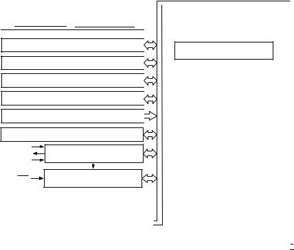
MCU Block Diagram
Figure 1 shows the structure of the MC68HC908AZ60.
3-gen |
|
MC68HC908AZ60 — Rev 2.0 |
|
|
|
MOTOROLA |
General Description |
13 |

14 |
MC68HC908AZ60 |
|
0.2 Rev — |
Description General
MOTOROLA |
gen-4 |
M68HC08 CPU
CPU |
|
ARITHMETIC/LOGIC |
REGISTERS |
|
UNIT (ALU) |
|
|
|
CONTROL AND STATUS REGISTERS — 62 BYTES
USER FLASH — 60 kBYTES
USER RAM — 2048BYTES
USER EEPROM — 1024 BYTES
MONITOR ROM — 224 BYTES
USER FLASH VECTOR SPACE — 52 BYTES
OSC1
OSC2 CLOCK GENERATOR
MODULE
CGMXFC
RST |
SYSTEM INTEGRATION |
|||||
MODULE |
||||||
|
|
|
|
|
||
|
|
|
|
|
|
|
|
IRQ |
|
|
|
IRQ MODULE |
|
|
|
|
|
|
||
|
|
|
|
|
|
|
|
|
|
|
|
|
|
|
|
|
|
|
POWER-ON RESET |
|
|
|
|
|
|
MODULE |
|
|
|
|
|
|
|
|
VSS |
|
|
|
|
|
|
|
VDD |
|
|
POWER |
|
|||
VDDA |
|
|
|
VSSA |
|
|
|
|
|
|
|
|
|
|
VREFH
ANALOG-TO-DIGITAL
MODULE
BREAK MODULE
LOW-VOLTAGE INHIBIT
MODULE
COMPUTER OPERATING
PROPERLY MODULE
TIMER A 6 CHANNEL
INTERFACE MODULE
TIMER B INTERFACE
MODULE
SERIAL COMMUNICATIONS
INTERFACE MODULE
SERIAL PERIPHERAL
INTERFACE MODULE
KEYBOARD INTERRUPT
MODULE
PROGRAMMABLE INTERRUPT
TIMER (PIT) MODULE
 AVSS/VREFL
VDDAREF
DDRA |
PTA |
PTA7–PTA0 |


 DDRH DDRG DDRF DDRE DDRD DDRC DDRB
PTB |
PTB7/ATD7–PTB0/ATD0 |
|
|
||
PTC |
PTC5–PTC3 |
|
PTC2/MCLK |
||
|
||
|
PTC1–PTC0 |
|
|
PTD7 |
|
|
PTD6/ATD14/TACLK |
|
PTD |
PTD5/ATD13 |
|
PTD4/ATD12/TBCLK |
||
|
PTD3/ATD11 |
|
|
PTD2/ATD10 |
|
|
PTD1/ATD9–PTD0/ATD8 |
|
|
PTE7/SPSCK |
|
|
PTE6/MOSI |
|
|
PTE5/MISO |
|
PTE |
PTE4/SS |
|
PTE3/TACH1 |
||
|
PTE2/TACH0 |
|
|
PTE1/RxD |
|
|
PTE0/TxD |
|
|
PTF6 |
|
PTF |
PTF5/TBCH1–PTF4/TBCH0 |
|
PTF3/TACH5-PTF2/TACH4 |
||
|
||
|
PTF1/TACH3 |
|
|
PTF0/TACH2 |
|
PTG |
PTG2/KBD2–PTG0/KBD0 |
|
|
||
PTH |
PTH1/KBD4–PTH0/KBD3 |
|
|
CANRx
MSCAN MODULE
CANTx
Figure 1. MCU Block Diagram for the MC68HC908AZ60 (64-Pin QFP)
Description General

General Description
Pin Assignments
Pin Assignments
Figure 2 shows the MC68HC908AZ60 pin assignments.
PTC4 1
IRQ
RST
PTF0/TACH2
PTF1/TACH3
PTF2/TACH4
PTF3/TACH5
PTF4/TBCH0
CANRx
CANTx
PTF5/TBCH1
PTF6
PTE0/TxD
PTE1/RxD
PTE2/TACH0
PTE3/TACH1 16
|
PTC5 |
PTC3 |
PTC2/MCLK |
PTC1 |
PTC0 |
OSC1 |
OSC2 |
CGMXFC |
V |
V |
V |
PTD7 |
PTD6/ATD14/TACLK |
PTD5/ATD13 |
PTD4/ATD12/TBCLK |
||||||||||||||
|
|
|
|
|
|
|
|
|
|
|
|
|
|
|
|
|
SSA |
DDA |
REFH |
|
|
|
|
|
|
|
|||
|
64 |
|
|
|
|
|
|
|
|
|
|
|
|
|
|
|
|
|
|
|
|
|
|
|
|
|
|
|
|
|
|
|
63 |
|
62 |
|
61 |
|
60 |
|
59 |
|
58 |
|
57 |
|
56 |
|
55 |
|
54 |
|
53 |
|
52 |
|
51 |
|
50 |
2 |
|
|
|
|
|
|
|
|
|
|
|
|
|
|
|
|
|
|
|
|
|
|
|
|
|
|
|
|
|
3 |
|
|
|
|
|
|
|
|
|
|
|
|
|
|
|
|
|
|
|
|
|
|
|
|
|
|
|
|
|
4 |
|
|
|
|
|
|
|
|
|
|
|
|
|
|
|
|
|
|
|
|
|
|
|
|
|
|
|
|
|
5 |
|
|
|
|
|
|
|
|
|
|
|
|
|
|
|
|
|
|
|
|
|
|
|
|
|
|
|
|
|
6 |
|
|
|
|
|
|
|
|
|
|
|
|
|
|
|
|
|
|
|
|
|
|
|
|
|
|
|
|
|
7 |
|
|
|
|
|
|
|
|
|
|
|
|
|
|
|
|
|
|
|
|
|
|
|
|
|
|
|
|
|
8 |
|
|
|
|
|
|
|
|
|
|
|
|
|
|
|
|
|
|
|
|
|
|
|
|
|
|
|
|
|
9 |
|
|
|
|
|
|
|
|
|
|
|
|
|
|
|
|
|
|
|
|
|
|
|
|
|
|
|
|
|
10 |
|
|
|
|
|
|
|
|
|
|
|
|
|
|
|
|
|
|
|
|
|
|
|
|
|
|
|
|
|
11 |
|
|
|
|
|
|
|
|
|
|
|
|
|
|
|
|
|
|
|
|
|
|
|
|
|
|
|
|
|
12 |
|
|
|
|
|
|
|
|
|
|
|
|
|
|
|
|
|
|
|
|
|
|
|
|
|
|
|
|
|
13 |
|
|
|
|
|
|
|
|
|
|
|
|
|
|
|
|
|
|
|
|
|
|
|
|
|
|
|
|
|
14 |
|
|
|
|
|
|
|
|
|
|
|
|
|
|
|
|
|
|
|
|
|
|
|
|
|
|
|
|
|
15 |
|
|
|
|
|
|
|
|
|
|
|
|
|
|
|
|
|
|
|
|
|
|
|
|
|
|
|
|
|
|
|
|
18 |
|
19 |
|
20 |
|
21 |
|
22 |
|
23 |
|
24 |
|
25 |
|
26 |
|
27 |
|
28 |
|
29 |
|
30 |
|
31 |
|
|
|
|
|
|
|
|
|
|
|
|
|
|
|
|
|
|
|
|
|
|
|
|
|
|
|
|
|
|
|
17 |
|
|
|
|
|
|
|
|
|
|
|
|
|
|
|
|
|
|
|
|
|
|
|
|
|
|
|
|
|
PTE4/SS |
PTE5/MISO |
PTE6/MOSI |
PTE7/SPSCK |
V |
V |
PTG0/KBD0 |
PTG1/KBD1 |
PTG2/KBD2 |
PTA0 |
PTA1 |
PTA2 |
PTA3 |
PTA4 |
PTA5 |
||||||||||||||
|
|
|
|
|
|
|
|
|
SS |
DD |
|
|
|
|
|
|
|
|
|
|
|
|
|
|
|
|
|
||
PTH1/KBD4 |
|
|
49 |
|
|
|
48 |
PTH0/KBD3 |
47 |
|
PTD3/ATD11 |
46 |
|
PTD2/ATD10 |
45 |
|
AVSS /VREFL |
44 |
|
VDDAREF |
43 |
|
PTD1/ATD9 |
42 |
|
PTD0/ATD8 |
41 |
|
PTB7/ATD7 |
|
|
|
40 |
|
PTB6/ATD6 |
39 |
|
PTB5/ATD5 |
38 |
|
PTB4/ATD4 |
37 |
|
PTB3/ATD3 |
36 |
|
PTB2/ATD2 |
35 |
|
PTB1/ATD1 |
34 |
|
PTB0/ATD0 |
|
33 |
PTA7 |
32 |
|
|
|
|
|
PTA6 |
|
|
|
Figure 2. MC68HC908AZ60 (64-Pin QFP) |
|
NOTE: |
The following pin descriptions are just a quick reference. For a more |
|
|
detailed representation, see I/O Ports on page 305. |
|
5-gen |
MC68HC908AZ60 — Rev 2.0 |
|
|
|
|
|
|
|
MOTOROLA |
General Description |
15 |
General Description
Power Supply Pins |
VDD and VSS are the power supply and ground pins. The MCU operates |
(VDD and VSS) |
from a single power supply. |
|
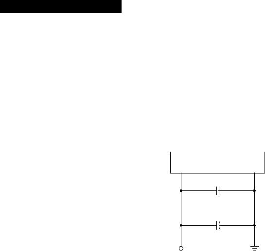
Fast signal transitions on MCU pins place high, short-duration current |
|
demands on the power supply. To prevent noise problems, take special |
|
care to provide power supply bypassing at the MCU as shown in Figure |
|
3. Place the C1 bypass capacitor as close to the MCU as possible. Use |
|
a high-frequency response ceramic capacitor for C1. C2 is an optional |
|
bulk current bypass capacitor for use in applications that require the port |
|
pins to source high current levels. |
MCU
VDD |
VSS |
C1
0.1 F
+
C2
VDD
NOTE: Component values shown represent typical applications.
Figure 3. Power supply bypassing
VSS is also the ground for the port output buffers and the ground return for the serial clock in the serial peripheral interface module (SPI). See
Serial Peripheral Interface Module (SPI) on page 237.
NOTE: VSS must be grounded for proper MCU operation.
Oscillator Pins |
The OSC1 and OSC2 pins are the connections for the on-chip oscillator |
(OSC1 and OSC2) |
circuit. See Clock Generator Module (CGM) on page 127. |
MC68HC908AZ60 — Rev 2.0 |
|
6-gen |
|
|
|
16 |
General Description |
MOTOROLA |
|
|
|
|
|
|
|
|
|
General Description |
|||
|
|
|
|
|
|
|
|
|
Pin Assignments |
|||
External Reset Pin |
A logic 0 on the |
|
pin forces the MCU to a known startup state. |
|
|
|||||||
RST |
RST |
|||||||||||
|
|
|
|
|
is bidirectional, allowing a reset of the entire system. It is driven low when |
|||||||
(RST) |
||||||||||||
|
|
|
|
|
|
any internal reset source is asserted. See |
|
|
||||
|
|
|
|
|
|
System Integration Module (SIM) on page 105 for more information. |
||||||
External Interrupt |
|
is an asynchronous external interrupt pin. See |
|
|
||||||||
IRQ |
|
|
||||||||||
Pin |
|
|
External Interrupt Module (IRQ) on page 191. |
|
|
|||||||
(IRQ) |
|
|
||||||||||
Analog Power |
VDDA is the power supply pin for the analog portion of the chip. This pin |
|||||||||||
Supply Pin (VDDA) |
will supply the clock generator module (CGM). See |
|
|
|||||||||
|
|
|
|
|
|
Clock Generator Module (CGM) on page 127. |
|
|
||||
Analog Ground |
The VSSA analog ground pin is used only for the ground connections for |
|||||||||||
Pin (VSSA) |
the analog sections of the circuit and should be decoupled as per the |
|
|
|||||||||
|
|
|
|
|
|
VSS digital ground pin. The analog sections consist of a clock generator |
||||||
|
|
|
|
|
|
module (CGM). See Clock Generator Module (CGM) on page 127. |
|
|
||||
External Filter |
CGMXFC is an external filter capacitor connection for the CGM. See |
|
|
|||||||||
Capacitor Pin |
Clock Generator Module (CGM) on page 127 |
|
|
|||||||||
(CGMXFC) |
|
|
|
|
|
|
|
|||||
Port A |
PTA7–PTA0 are general-purpose bidirectional I/O port pins. See I/O |
|
|
|||||||||
Input/Output (I/O) |
Ports on page 305. |
|
|
|||||||||
Pins (PTA7–PTA0) |
|
|
|
|
|
|
|
|||||
Port B I/O Pins |
Port B is an 8-bit special function port that shares all eight pins with the |
|||||||||||
(PTB7/ATD7ÐPTB0/ |
analog-to-digital converter (ADC). See |
|
|
|||||||||
ATD0) |
Analog-to-Digital Converter (ADC-15) on page 421 and I/O Ports on |
|||||||||||
|
|
|
|
|
|
page 305. |
|
|
||||
Port C I/O Pins |
PTC5–PTC3 and PTC1–PTC0 are general-purpose bidirectional I/O |
|
|
|||||||||
(PTC5ÐPTC0) |
port pins. PTC2/MCLK is a special function port that shares its pin with |
|||||||||||
|
7-gen |
|
|
|
MC68HC908AZ60 — Rev 2.0 |
|||||||
|
|
|
|
|
|
|
|
|
|
|
|
|
|
|
|
|
|
|
|
|
|
|
|
|
|
|
MOTOROLA |
|
General Description |
17 |
||||||||

General Description
|
the system clock which has a frequency equivalent to the system clock. |
|
See I/O Ports on page 305. |
Port D I/O Pins |
Port D is an 8-bit special-function port that shares seven of its pins with |
(PTD7ÐPTD0/ATD8) |
the analog-to-digital converter module (ADC-15), one of its pins with the |
|
timer interface module (TIMA), and one more of its pins with the timer |
|
interface module (TIMB). See Timer Interface Module A (TIMA-6) on |
|
page 389, Analog-to-Digital Converter (ADC-15) on page 421 and I/O |
|
Ports on page 305. |
Port E I/O Pins |
Port E is an 8-bit special function port that shares two of its pins with the |
(PTE7/SPSCKÐPTE0/ |
timer interface module (TIMA), four of its pins with the serial peripheral |
TxD) |
interface module (SPI), and two of its pins with the serial communication |
|
interface module (SCI). See |
|
Serial Communications Interface Module (SCI) on page 199, |
|
Serial Peripheral Interface Module (SPI) on page 237, |
|
Timer Interface Module A (TIMA-6) on page 389, and I/O Ports on |
|
page 305. |
Port F I/O Pins |
Port F is a 7-bit special function port that shares its pins with the timer |
(PTF6ÐPTF0/TACH2) |
interface module (TIMB). Six of its pins are shared with the timer |
|
interface module (TIMA-6). See Timer Interface Module A (TIMA-6) on |
|
page 389, Timer Interface Module B (TIMB) on page 269, and I/O |
|
Ports on page 305. |
Port G I/O Pins |
Port G is a 3-bit special function port that shares all of its pins with the |
(PTG2/KBD2ÐPTG0 |
keyboard interrupt module (KBD). See Keyboard Module (KBD) on |
/KBD0) |
page 381 and I/O Ports on page 305. |
Port H I/O Pins |
Port H is a 2-bit special-function port that shares all of its pins with the |
(PTH1/KBD4ÐPTH0/ |
keyboard interrupt module (KBD). See Keyboard Module (KBD) on |
KBD3) |
page 381 and I/O Ports on page 305. |
MC68HC908AZ60 — Rev 2.0 |
|
8-gen |
|
|
|
18 |
General Description |
MOTOROLA |
|
General Description |
|
Pin Assignments |
CAN Transmit Pin |
This pin is the digital output from the CAN module (CANTx). See |
(CANTx) |
MSCAN Controller (MSCAN08) on page 331. |
CAN Receive Pin |
This pin is the digital input to the CAN module (CANRx). See MSCAN |
(CANRx) |
Controller (MSCAN08) on page 331. |
Table 1. External Pins Summary
|
Pin Name |
Function |
Driver |
Hysteresis |
Reset State |
|
||
|
Type |
(note 1) |
|
|||||
|
|
|
|
|
|
|
||
|
|
|
|
|
|
|
||
|
|
|
|
|
|
|
||
|
PTA7–PTA0 |
General-Purpose I/O |
Dual State |
No |
Input Hi-Z |
|
||
|
|
|
|
|
|
|
|
|
|
PTB7/ATD7–PTB0/ATD0 |
General-Purpose I/O |
Dual State |
No |
Input Hi-Z |
|
||
|
ADC Channel |
|
||||||
|
|
|
|
|
|
|
|
|
|
|
|
|
|
|
|
||
|
PTC5–PTC0 |
General-Purpose I/O |
Dual State |
No |
Input Hi-Z |
|
||
|
|
|
|
|
|
|
||
|
PTD7 |
General Purpose I/O/ |
Dual State |
No |
Input Hi-Z |
|
||
|
|
|
|
|
|
|
|
|
|
|
|
|
General-Purpose I/O |
|
|
|
|
|
PTD6/ATD14/TACLK ADC Channel |
ADC Channel/Timer |
Dual State |
No |
Input Hi-Z |
|
||
|
|
|
|
External Input Clock |
|
|
|
|
|
|
|
|
|
|
|
||
|
PTD5/ATD13 ADC Channel |
General-Purpose I/O |
Dual State |
No |
Input Hi-Z |
|
||
|
|
|
|
ADC Channel |
|
|||
|
|
|
|
|
|
|
|
|
|
|
|
|
|
|
|
|
|
|
PTD4/ATD12/TBCLK ADC Channel |
General-Purpose I/O |
|
|
Input Hi-Z |
|
||
|
ADC Channel/Timer |
Dual State |
No |
|
||||
|
|
|
|
|
|
|||
|
|
|
|
External Input Clock |
|
|
|
|
|
|
|
|
|
|
|
|
|
|
PTD3/ATD11–PTD0/ATD8 ADC Channels |
General-Purpose I/O |
Dual State |
No |
Input Hi-Z |
|
||
|
ADC Channel |
|
|
|
||||
|
|
|
|
|
|
|
|
|
|
|
|
|
|
|
|
|
|
|
PTE7/SPSCK |
General-Purpose I/O |
Dual State |
Yes |
Input Hi-Z |
|
||
|
SPI Clock |
Open Drain |
|
|||||
|
|
|
|
|
|
|
||
|
|
|
|
|
|
|
|
|
|
PTE6/MOSI |
General-Purpose I/O |
Dual State |
Yes |
Input Hi-Z |
|
||
|
SPI Data Path |
Open Drain |
|
|||||
|
|
|
|
|
|
|
||
|
|
|
|
|
|
|
|
|
|
PTE5/MISO |
General-Purpose I/O |
Dual State |
Yes |
Input Hi-Z |
|
||
|
SPI Data Path |
Open Drain |
|
|||||
|
|
|
|
|
|
|
||
|
|
|
|
|
|
|
|
|
|
|
|
|
General-Purpose I/O |
|
|
|
|
|
PTE4/SS |
Dual State |
Yes |
Input Hi-Z |
|
|||
|
SPI Slave Select |
|
||||||
|
|
|
|
|
|
|
|
|
|
|
|
|
|
|
|
|
|
|
PTE3/TACH1 |
General-Purpose I/O |
Dual State |
Yes |
Input Hi-Z |
|
||
|
Timer Channel 1 |
|
||||||
|
|
|
|
|
|
|
|
|
|
|
|
|
|
|
|
|
|
|
PTE2/TACH0 |
General-Purpose I/O |
Dual State |
Yes |
Input Hi-Z |
|
||
|
Timer Channel 0 |
|
||||||
|
|
|
|
|
|
|
|
|
|
|
|
|
|
|
|
|
|
|
PTE1/RxD |
General-Purpose I/O |
Dual State |
Yes |
Input Hi-Z |
|
||
|
SCI Receive Data |
|
||||||
|
|
|
|
|
|
|
|
|
|
|
|
|
|
|
|
||
|
9-gen |
|
|
MC68HC908AZ60 — Rev 2.0 |
||||
|
|
|
|
|
|
|
|
|
|
|
|
|
|
|
|
|
|
|
MOTOROLA |
General Description |
|
|
19 |
|||

General Description
Table 1. External Pins Summary (Continued)
|
Pin Name |
Function |
Driver |
Hysteresis |
Reset State |
|
||||
|
Type |
(note 1) |
|
|||||||
|
|
|
|
|
|
|
|
|
||
|
|
|
|
|
|
|
|
|
|
|
|
|
|
|
|
|
|
|
|
|
|
|
PTE0/TxD |
General-Purpose I/O |
Dual State |
No |
Input Hi-Z |
|
||||
|
SCI Transmit Data |
|
||||||||
|
|
|
|
|
|
|
|
|
|
|
|
|
|
|
|
|
|
||||
|
PTF6 |
General-Purpose I/O |
Dual State |
No |
Input Hi-Z |
|
||||
|
|
|
|
|
|
|
|
|
|
|
|
PTF5/TBCH1–PTF4/TBCH0 |
General-Purpose |
Dual State |
Yes |
Input Hi-Z |
|
||||
|
I/O/Timer B Channel |
|
||||||||
|
|
|
|
|
|
|
|
|
|
|
|
|
|
|
|
|
|
|
|
|
|
|
PTF3/TACH5 |
General-Purpose I/O |
Dual State |
Yes |
Input Hi-Z |
|
||||
|
Timer A Channel 5 |
|
||||||||
|
|
|
|
|
|
|
|
|
|
|
|
|
|
|
|
|
|
|
|
|
|
|
PTF2/TACH4 |
General-Purpose I/O |
Dual State |
Yes |
Input Hi-Z |
|
||||
|
Timer A Channel 4 |
|
||||||||
|
|
|
|
|
|
|
|
|
|
|
|
|
|
|
|
|
|
|
|
|
|
|
PTF1/TACH3 |
General-Purpose I/O |
Dual State |
Yes |
Input Hi-Z |
|
||||
|
Timer A Channel 3 |
|
||||||||
|
|
|
|
|
|
|
|
|
|
|
|
|
|
|
|
|
|
|
|
|
|
|
PTF0/TACH2 |
General-Purpose I/O |
Dual State |
Yes |
Input Hi-Z |
|
||||
|
Timer A Channel 2 |
|
||||||||
|
|
|
|
|
|
|
|
|
|
|
|
|
|
|
|
|
|
|
|
|
|
|
PTG2/KBD2–PTG0/KBD0 |
General-Purpose I/O/ |
Dual State |
Yes |
Input Hi-Z |
|
||||
|
Keyboard Wakeup Pin |
|
||||||||
|
|
|
|
|
|
|
|
|
|
|
|
|
|
|
|
|
|
|
|
|
|
|
PTH1/KBD4 –PTH0/KBD3 |
General-Purpose I/O/ |
Dual State |
Yes |
Input Hi-Z |
|
||||
|
Keyboard Wakeup Pin |
|
||||||||
|
|
|
|
|
|
|
|
|
|
|
|
|
|
|
|
|
|
|
|||
|
|
VDD |
Chip Power Supply |
N/A |
N/A |
N/A |
|
|||
|
|
|
VSS |
Chip Ground |
N/A |
N/A |
N/A |
|
||
|
|
|
|
|
|
ADC Power Supply/ |
|
|
|
|
|
VDDAREF |
ADC Reference |
N/A |
N/A |
N/A |
|
||||
|
|
|
|
|
|
Voltage |
|
|
|
|
|
|
|
|
|
|
|
|
|
|
|
|
AVSS/VREFL |
ADC Ground/ADC |
N/A |
N/A |
N/A |
|
||||
|
Reference Voltage |
|
||||||||
|
VREFH |
A/D Reference |
N/A |
N/A |
N/A |
|
||||
|
Voltage |
|
||||||||
|
OSC1 |
External Clock In |
N/A |
N/A |
Input Hi-Z |
|
||||
|
|
|
|
|
|
|
||||
|
OSC2 |
External Clock Out |
N/A |
N/A |
Output |
|
||||
|
|
|
|
|
|
|
||||
|
CGMXFC |
PLL Loop Filter Cap |
N/A |
N/A |
N/A |
|
||||
|
|
|
|
|
|
|
|
|
|
|
|
|
|
|
|
|
External Interrupt |
|
|
|
|
|
|
IRQ |
N/A |
N/A |
Input Hi-Z |
|
||||
|
|
Request |
|
|||||||
|
|
|
|
|
|
|
|
|
|
|
|
|
|
|
|
|
|
|
|
||
|
|
|
|
|
|
Reset |
N/A |
N/A |
Output Low |
|
|
RST |
|||||||||
|
|
|
|
|
|
|
||||
|
CANRx |
CAN Serial Input |
N/A |
Yes |
Input Hi-Z |
|
||||
|
|
|
|
|
|
|
||||
|
CANTx |
CAN Serial Output |
Output |
No |
Output |
|
||||
|
|
|
|
|
|
|
||||
|
MC68HC908AZ60 — Rev 2.0 |
|
|
|
10-gen |
|||||
|
|
|
|
|
|
|
|
|
|
|
|
|
|
|
|
|
|
|
|
|
|
|
20 |
|
|
|
|
General Description |
|
|
MOTOROLA |
|
|
|
General Description |
|
|
|
Pin Assignments |
|
|
Table 2. Clock Source Summary |
||
|
|
|
|
Module |
|
Clock Source |
|
|
|
|
|
ADC |
|
CGMXCLK or Bus Clock |
|
|
|
|
|
CAN |
|
CGMXCLK or CGMOUT |
|
|
|
|
|
COP |
|
CGMXCLK |
|
|
|
|
|
CPU |
|
Bus Clock |
|
|
|
|
|
EEPROM |
|
RC OSC or Bus Clock |
|
|
|
|
|
SPI |
|
Bus Clock/SPSCK |
|
|
|
|
|
SCI |
|
CGMXCLK |
|
|
|
|
|
TIMA-6 |
|
Bus Clock or PTD6/ATD14/TACLK |
|
|
|
|
|
TIMB |
|
Bus Clock or PTD4/TBCLK |
|
|
|
|
|
PIT |
|
Bus Clock |
|
|
|
|
|
SIM |
|
CGMOUT and CGMXCLK |
|
|
|
|
|
IRQ |
|
Bus Clock |
|
|
|
|
|
BRK |
|
Bus Clock |
|
|
|
|
|
LVI |
|
Bus Clock |
|
|
|
|
|
CGM |
|
OSC1 and OSC2 |
|
|
|
|
|
Note 1: Hysteresis is not 100% tested but is typically a minimum of 300mV
11-gen |
|
MC68HC908AZ60 — Rev 2.0 |
|
|
|
MOTOROLA |
General Description |
21 |

General Description
Ordering Information
This section contains instructions for ordering the MC68HC908AZ60.
MC Order
Numbers
|
Table 3. MC Order Numbers |
||
|
|
|
|
MC Order Number |
Operating |
||
Temperature Range |
|||
|
|
||
|
|
|
|
MC68HC908AZ60CFU |
|
–40 °C to + 85°C |
|
|
|
|
|
MC68HC908AZ60VFU |
|
–40 °C to + 105 °C |
|
|
|
|
|
MC68HC908AZ60MFU |
|
–40 °C to + 125 °C |
|
|
|
|
|
MC68HC908AZ60 — Rev 2.0 |
|
12-gen |
|
|
|
22 |
General Description |
MOTOROLA |

Memory Map
Memory Map
Contents
Introduction . . . . . . . . . . . . . . . . . . . . . . . . . . . . . . . . . . . . . . . . . . . . . 23
I/O Section . . . . . . . . . . . . . . . . . . . . . . . . . . . . . . . . . . . . . . . . . . . . . 26
Introduction
The CPU08 can address 64 Kbytes of memory space. The memory map, shown in Figure 1, includes:
•60 Kbytes of FLASH EEPROM
•2048 Bytes of RAM
•1024 Bytes of EEPROM with Protect Option
•52 Bytes of User-Defined Vectors
•224 Bytes of Monitor ROM
The following definitions apply to the memory map representation of reserved and unimplemented locations.
•Reserved — Accessing a reserved location can have unpredictable effects on MCU operation.
•Unimplemented — Accessing an unimplemented location causes an illegal address reset if illegal address resets are enabled.
1-mem |
|
MC68HC908AZ60 — Rev 2.0 |
|
|
|
MOTOROLA |
Memory Map |
23 |

Memory Map
Figure 1. Memory Map
$0000 |
|
$0000 |
|
↓ |
I/O REGISTERS (64 BYTES) |
↓ |
|
$003F |
|
$003F |
|
$0040 |
|
$0040 |
|
|
|||
↓ |
I/O REGISTERS, 16 BYTES |
↓ |
|
$004F |
|
$004F |
|
$0050 |
|
$0050 |
|
|
|||
↓ |
RAM-1, 1024 BYTES |
↓ |
|
$044F |
|
$044F |
|
$0450 |
|
$0450 |
|
|
|||
↓ |
FLASH-2, 176 BYTES |
↓ |
|
$04FF |
|
$04FF |
|
$0500 |
|
$0500 |
|
CAN CONTROL AND MESSAGE |
|||
↓ |
↓ |
||
BUFFERS, 128 BYTES |
|||
$057F |
$057F |
||
|
|||
$0580 |
|
$0580 |
|
|
|||
↓ |
FLASH-2, 128 BYTES |
↓ |
|
$05FF |
|
$05FF |
|
$0600 |
|
$0600 |
|
|
|||
↓ |
EEPROM-2, 512 BYTES |
↓ |
|
$07FF |
|
$07FF |
|
$0800 |
|
$0800 |
|
|
|||
↓ |
EEPROM-1, 512 BYTES |
↓ |
|
$09FF |
|
$09FF |
|
$0A00 |
|
$0A00 |
|
|
|||
↓ |
RAM-2 , 1024 BYTES |
↓ |
|
$0DFF |
|
$0DFF |
|
$0E00 |
|
$0E00 |
|
|
|||
↓ |
FLASH-2, 29,184 BYTES |
↓ |
|
$7FFF |
|
$7FFF |
|
$8000 |
|
$8000 |
|
|
|||
↓ |
FLASH-1, 32,256BYTES |
↓ |
|
$FDFF |
|
$FDFF |
|
|
|
|
|
$FE00 |
SIM BREAK STATUS REGISTER (SBSR) |
$FE00 |
|
|
|
|
|
$FE01 |
SIM RESET STATUS REGISTER (SRSR) |
$FE01 |
|
|
|
|
|
$FE02 |
RESERVED |
$FE02 |
|
|
|
|
|
$FE03 |
SIM BREAK FLAG CONTROL REGISTER (SBFCR) |
$FE03 |
|
|
|
|
|
MC68HC908AZ60 — Rev 2.0 |
|
2-mem |
|
|
|
|
|
|
|
|
|
24 |
Memory Map |
MOTOROLA |
|
|
Memory Map |
|
|
|
Introduction |
|
|
Figure 1. Memory Map (Continued) |
|
|
|
|
|
|
$FE04 |
RESERVED |
$FE04 |
|
|
|
|
|
$FE05 |
RESERVED |
$FE05 |
|
|
|
|
|
$FE06 |
UNIMPLEMENTED |
$FE06 |
|
|
|
|
|
$FE07 |
RESERVED |
$FE07 |
|
|
|
|
|
$FE08 |
RESERVED |
$FE08 |
|
|
|
|
|
$FE09 |
CONFIGURATION WRITE-ONCE REGISER |
$FE09 |
|
(CONFIG-2) |
|||
|
|
||
|
|
|
|
$FE0A |
RESERVED |
$FE0A |
|
|
|
|
|
$FE0B |
FLASH CONTROL REGISTER (FLCR1) |
$FE0B |
|
|
|
|
|
$FE0C |
BREAK ADDRESS REGISTER HIGH (BRKH) |
$FE0C |
|
|
|
|
|
$FE0D |
BREAK ADDRESS REGISTER LOW (BRKL) |
$FE0D |
|
|
|
|
|
$FE0E |
BREAK STATUS AND CONTROL REGISTER (BSCR) |
$FE0E |
|
|
|
|
|
$FE0F |
LVI STATUS REGISTER (LVISR) |
$FE0F |
|
|
|
|
|
$FE10 |
RESERVED |
$FE10 |
|
|
|
|
|
$FE11 |
FLASH CONTROL REGISTER (FLCR2) |
$FE11 |
|
|
|
|
|
$FE12 |
|
$FE12 |
|
↓ |
UNIMPLEMENTED (5BYTES) |
↓ |
|
$FE17 |
|
$FE17 |
|
|
|
|
|
$FE18 |
EEPROM NON-VOLATILE REGISTER (EENVR2) |
$FE18 |
|
|
|
|
|
$FE19 |
EEPROM CONTROL REGISTER (EECR2) |
$FE19 |
|
|
|
|
|
$FE1A |
RESERVED |
$FE1A |
|
|
|
|
|
$FE1B |
EEPROM ARRAY CONFIGURATION (EEACR2) |
$FE1B |
|
|
|
|
|
$FE1C |
EEPROM NON-VOLATILE REGISTER (EENVR1) |
$FE1C |
|
|
|
|
|
$FE1D |
EEPROM CONTROL REGISTER (EECR1) |
$FE1D |
|
|
|
|
|
$FE1E |
RESERVED |
$FE1E |
|
|
|
|
|
$FE1F |
EEPROM ARRAY CONFIGURATION (EEACR1) |
$FE1F |
|
$FE20 |
|
$FE20 |
|
|
|||
↓ |
MONITOR ROM (224 BYTES) |
↓ |
|
$FEFF |
|
$FEFF |
|
|
|
|
|
$FF00 |
|
$FF00 |
|
↓ |
UNIMPLEMENTED (128 BYTES) |
↓ |
|
$FF7F |
|
$FF7F |
|
|
|
|
|
$FF80 |
FLASH BLOCK PROTECT REGISTER (FLBPR1) |
$FF80 |
|
|
|
|
|
$FF81 |
FLASH BLOCK PROTECT REGISTER (FLBPR2) |
$FF81 |
|
$FF82 |
|
$FF82 |
|
|
|||
↓ |
RESERVED (75 BYTES) |
↓ |
|
$FFCB |
|
$FFCB |
|
|
|
|
|
3-mem |
MC68HC908AZ60 — Rev 2.0 |
||
|
|
|
|
|
|
|
|
MOTOROLA |
Memory Map |
25 |
|

Memory Map
Figure 1. Memory Map (Continued)
$FFCC |
|
$FFCC |
↓ |
VECTORS (52BYTES) |
↓ |
$FFFF |
|
$FFFF |
|
|
|
I/O Section
Addresses $0000–$003F, shown in Figure 2, contain most of the control, status, and data registers. Additional I/O registers have these addresses:
•$FE00 (SIM break status register, SBSR)
•$FE01 (SIM reset status register, SRSR)
•$FE03 (SIM break flag control register, SBFCR)
•$FE09 (configuration write-once register, CONFIG-2)
•$FE0B (FLASH control register, FLCR1)
•$FE0C and $FE0D (break address registers, BRKH and BRKL)
•$FE0E (break status and control register, BRKSCR)
•$FE0F (LVI status register, LVISR)
•$FE11 (FLASH control register, FLCR2)
•$FE18 (EEPROM non-volatile register, EENVR2)
•$FE19 (EEPROM control register, EECR2)
•$FE1B (EEPROM array configuration register, EEACR2)
•$FE1C (EEPROM non-volatile register, EENVR1)
•$FE1D (EEPROM control register, EECR1)
•$FE1F (EEPROM array configuration register, EEACR1)
•$FF80 (FLASH block protect register, FLBPR1)
•$FF81 (FLASH block protect register, FLBPR2)
•$FFFF (COP control register, COPCTL)
Table 1 is a list of vector locations.
MC68HC908AZ60 — Rev 2.0 |
|
4-mem |
|
|
|
26 |
Memory Map |
MOTOROLA |
Memory Map
I/O Section
Addr. |
Register Name |
Bit 7 |
6 |
5 |
4 |
3 |
2 |
1 |
Bit 0 |
$0000
$0001
$0002
$0003
$0004
$0005
$0006
$0007
$0008
$0009
$000A
$000B
$000C
$000D
$000E
$000F
$0010
Read:
Port A Data Register (PTA)
Write:
Read:
Port B Data Register (PTB)
Write:
Read:
Port C Data Register (PTC)
Write:
Read:
Port D Data Register (PTD)
Write:
Data Direction Register A Read:
(DDRA) Write:
Data Direction Register B Read:
(DDRB) Write:
Data Direction Register C Read:
(DDRC) Write:
Data Direction Register D Read:
(DDRD) Write:
Read:
Port E Data Register (PTE)
Write:
Read:
Port F Data Register (PTF)
Write:
Read:
Port G Data Register (PTG)
Write:
Read:
Port H Data Register (PTH)
Write:
Data Direction Register E Read:
(DDRE) Write:
Data Direction Register F Read:
(DDRF) Write:
Data Direction Register G Read:
(DDRG) Write:
Data Direction Register H Read:
(DDRH) Write:
Read:
SPI Control Register (SPCR)
Write:
PTA7 |
PTA6 |
PTA5 |
PTA4 |
PTA3 |
PTA2 |
PTA1 |
PTA0 |
|
|
|
|
|
|
|
|
PTB7 |
PTB6 |
PTB5 |
PTB4 |
PTB3 |
PTB2 |
PTB1 |
PTB0 |
|
|
|
|
|
|
|
|
0 |
0 |
PTC5 |
PTC4 |
PTC3 |
PTC2 |
PTC1 |
PTC0 |
|
|
||||||
|
|
||||||
|
|
|
|
|
|
|
|
PTD7 |
PTD6 |
PTD5 |
PTD4 |
PTD3 |
PTD2 |
PTD1 |
PTD0 |
|
|
|
|
|
|
|
|
DDRA7 |
DDRA6 |
DDRA5 |
DDRA4 |
DDRA3 |
DDRA2 |
DDRA1 |
DDRA0 |
|
|
|
|
|
|
|
|
DDRB7 |
DDRB6 |
DDRB5 |
DDRB4 |
DDRB3 |
DDRB2 |
DDRB1 |
DDRB0 |
|
|
|
|
|
|
|
|
MCLKEN |
0 |
DDRC5 |
DDRC4 |
DDRC3 |
DDRC2 |
DDRC1 |
DDRC0 |
|
|||||||
|
|||||||
|
|
|
|
|
|
|
|
DDRD7 |
DDRD6 |
DDRD5 |
DDRD4 |
DDRD3 |
DDR2 |
DDRD1 |
DDRD0 |
|
|
|
|
|
|
|
|
PTE7 |
PTE6 |
PTE5 |
PTE4 |
PTE3 |
PTE2 |
PTE1 |
PTE0 |
|
|
|
|
|
|
|
|
0 |
PTF6 |
PTF5 |
PTF4 |
PTF3 |
PTF2 |
PTF1 |
PTF0 |
|
|||||||
|
|||||||
|
|
|
|
|
|
|
|
0 |
0 |
0 |
0 |
0 |
PTG2 |
PTG1 |
PTG0 |
|
|
|
|
|
|||
|
|
|
|
|
|||
|
|
|
|
|
|
|
|
0 |
0 |
0 |
0 |
0 |
0 |
PTH1 |
PTH0 |
|
|
|
|
|
|
||
|
|
|
|
|
|
||
|
|
|
|
|
|
|
|
DDRE7 |
DDRE6 |
DDRE5 |
DDRE4 |
DDRE3 |
DDRE2 |
DDRE1 |
DDRE0 |
|
|
|
|
|
|
|
|
0 |
DDRF6 |
DDRF5 |
DDRF4 |
DDRF3 |
DDRF2 |
DDRF1 |
DDRF0 |
|
|||||||
|
|||||||
|
|
|
|
|
|
|
|
0 |
0 |
0 |
0 |
0 |
DDRG2 |
DDRG1 |
DDRG0 |
|
|
|
|
|
|||
|
|
|
|
|
|||
|
|
|
|
|
|
|
|
0 |
0 |
0 |
0 |
0 |
0 |
DDRH1 |
DDRH0 |
|
|
|
|
|
|
||
|
|
|
|
|
|
||
|
|
|
|
|
|
|
|
SPRIE |
R |
SPMSTR |
CPOL |
CPHA |
SPWOM |
SPE |
SPTIE |
|
|
|
|
|
|
|
|
Figure 2. Control, Status, and Data Registers (Sheet 1 of 6)
5-mem |
|
MC68HC908AZ60 — Rev 2.0 |
|
|
|
MOTOROLA |
Memory Map |
27 |

Memory Map
Addr. |
Register Name |
Bit 7 |
6 |
5 |
|
4 |
3 |
2 |
1 |
Bit 0 |
|||
|
|
|
|
= Unimplemented |
|
R |
= Reserved |
|
|
||||
$0011 |
SPI Status and Control Read: |
SPRF |
ERRIE |
OVRF |
MODF |
SPTE |
MODFE |
SPR1 |
SPR0 |
|
|||
Register (SPSCR) Write: |
|
|
|
|
|
|
N |
|
|||||
|
|
|
|
|
|
|
|
|
|
|
|
||
|
|
Read: |
R7 |
R6 |
|
R5 |
R4 |
R3 |
R2 |
R1 |
R0 |
|
|
$0012 |
SPI Data Register (SPDR) |
|
|
|
|
|
|
|
|
|
|
|
|
T7 |
T6 |
|
T5 |
T4 |
T3 |
T2 |
T1 |
T0 |
|
||||
|
|
Write: |
|
|
|||||||||
|
|
Read: |
|
|
|
|
|
|
|
|
|
|
|
$0013 |
LOOPS |
ENSCI |
TXINV |
M |
WAKE |
ILTY |
PEN |
PTY |
|
||||
SCI Control Register 1 (SCC1) |
|
||||||||||||
|
|
Write: |
|
|
|
|
|
|
|
|
|
|
|
|
|
Read: |
|
|
|
|
|
|
|
|
|
|
|
$0014 |
SCTIE |
TCIE |
SCRIE |
ILIE |
TE |
RE |
RWU |
SBK |
|
||||
SCI Control Register 2 (SCC2) |
|
||||||||||||
|
|
Write: |
|
|
|
|
|
|
|
|
|
|
|
|
|
Read: |
R8 |
|
|
|
|
|
|
|
|
|
|
$0015 |
SCI Control Register 3 (SCC3) |
|
T8 |
|
R |
R |
ORIE |
NEIE |
FEIE |
PEIE |
|
||
|
|
Write: |
|
|
|
|
|
|
|
|
|
|
|
|
|
Read: |
SCTE |
TC |
SCRF |
IDLE |
OR |
NF |
FE |
PE |
|
||
$0016 |
SCI Status Register 1 (SCS1) |
|
|
|
|
|
|
|
|
|
|
|
|
|
|
Write: |
|
|
|
|
|
|
|
|
|
|
|
|
|
Read: |
0 |
0 |
0 |
|
0 |
0 |
0 |
BKF |
RPF |
|
|
$0017 |
SCI Status Register 2 (SCS2) |
|
|
|
|
|
|
|
|
|
|
|
|
|
|
Write: |
|
|
|
|
|
|
|
|
|
|
|
|
|
Read: |
R7 |
R6 |
|
R5 |
R4 |
R3 |
R2 |
R1 |
R0 |
|
|
$0018 |
SCI Data Register (SCDR) |
|
|
|
|
|
|
|
|
|
|
|
|
T7 |
T6 |
|
T5 |
T4 |
T3 |
T2 |
T1 |
T0 |
|
||||
|
|
Write: |
|
|
|||||||||
|
|
|
|
|
|
|
|
|
|
|
|
|
|
|
|
Read: |
0 |
0 |
|
|
|
|
|
|
|
|
|
$0019 |
SCI Baud Rate Register (SCBR) |
|
|
SCP1 |
SCP0 |
|
SCR2 |
SCR1 |
SCR0 |
|
|||
|
|
Write: |
|
|
|
|
|
|
|
|
|
|
|
$001A |
IRQ Status and Control Read: |
0 |
0 |
0 |
|
0 |
IRQF |
0 |
IMASK1 |
MODE1 |
|
||
Register (ISCR) Write: |
|
|
|
|
|
|
|
ACK1 |
|
||||
|
|
|
|
|
|
|
|
|
|
|
|
||
$001B |
Keyboard Status and Control Read: |
0 |
0 |
0 |
|
0 |
KEYF |
0 |
IMASKK |
MODEK |
|
||
Register (KBSCR) Write: |
|
|
|
|
|
|
|
ACKK |
|
||||
|
|
|
|
|
|
|
|
|
|
|
|
||
|
|
Read: |
|
PLLF |
|
|
|
|
1 |
1 |
1 |
1 |
|
$001C |
PLL Control Register (PCTL) |
PLLIE |
|
PLLON |
BCS |
|
|
|
|
|
|||
|
|
Write: |
|
|
|
|
|
|
|
|
|
|
|
|
|
PLL Bandwidth Control Read: |
|
LOCK |
|
|
|
|
0 |
0 |
0 |
0 |
|
$001D |
AUTO |
ACQ |
XLD |
|
|||||||||
Register (PBWC) Write: |
|
|
|
|
|
|
|||||||
|
|
|
|
|
|
|
|
|
|
|
|
|
|
$001E |
PLL Programming Register Read: |
MUL7 |
MUL6 |
MUL5 |
MUL4 |
VRS7 |
VRS6 |
VRS5 |
VRS4 |
|
|||
(PPG) Write: |
|
||||||||||||
|
|
|
|
|
|
|
|
|
|
|
|
|
|
$001F |
Configuration Write-Once Read: |
LVISTOP |
R |
LVIRST |
LVIPWR |
SSREC |
COPL |
STOP |
COPD |
|
|||
Register (CONFIG-1) Write: |
|
||||||||||||
|
|
|
|
|
|
|
|
|
|
|
|
|
|
$0020 |
Timer A Status and Control Read: |
TOF |
TOIE |
TSTOP |
0 |
0 |
PS2 |
PS1 |
PS0 |
|
|||
Register (TASC) Write: |
0 |
TRST |
|
|
|||||||||
|
|
|
|
|
|
|
|
|
|
|
|||
$0021 |
Keyboard Interrupt Enable Register Read: |
0 |
0 |
0 |
|
KBIE4 |
KBIE3 |
KBIE2 |
KBIE1 |
KBIE0 |
|
||
(KBIE) Write: |
|
|
|
|
|
|
|||||||
|
|
|
|
|
|
|
|
|
|
|
|
|
|
|
|
Figure 2. Control, Status, and Data Registers (Sheet 2 of 6) |
|
|
|
||||||||
|
MC68HC908AZ60 — Rev 2.0 |
|
|
|
|
|
|
|
|
|
6-mem |
||
|
|
|
|
|
|
|
|
|
|
|
|
|
|
|
|
|
|
|
|
|
|
|
|
|
|
|
|
28 |
|
|
Memory Map |
|
|
|
MOTOROLA |
||||||
 Loading...