


 Loading...
Motorola MC68HCP11A1P, MC68HCP11A1VFN, MC68HCP11A1VP, MC68HCP11A1MFN, MC68HC11A8FN1 Datasheet
...MOTOROLA
SEMICONDUCTOR
TECHNICAL DATA
Order this document by MC68HC11A8TS/D
MC68HC11A8
MC68HC11A1
MC68HC11A0
Technical Summary
8-Bit Microcontrollers
1 Introduction
The MC68HC11A8, MC68HC11A1, and MC68HC11A0 high-performance microcontroller units (MCUs) are based on the M68HC11 Family. These high speed, low power consumption chips have multiplexed buses and a fully static design. The chips can operate at frequencies from 3 MHz to dc. The three MCUs are created from the same masks; the only differences are the value stored in the CONFIG register, and whether or not the ROM or EEPROM is tested and guaranteed.
For detailed information about specific characteristics of these MCUs, refer to the M68HC11 Reference Manual (M68HC11RM/AD).
1.1Features
•M68HC11 CPU
•Power Saving STOP and WAIT Modes
•8 Kbytes ROM
•512 Bytes of On-Chip EEPROM
•256 Bytes of On-Chip RAM (All Saved During Standby)
•16-Bit Timer System
—3 Input Capture Channels
—5 Output Compare Channels
•8-Bit Pulse Accumulator
•Real-Time Interrupt Circuit
•Computer Operating Properly (COP) Watchdog System
•Synchronous Serial Peripheral Interface (SPI)
•Asynchronous Nonreturn to Zero (NRZ) Serial Communications Interface (SCI)
•8-Channel, 8-Bit Analog-to-Digital (A/D) Converter
•38 General-Purpose Input/Output (I/O) Pins
—15 Bidirectional I/O Pins
—11 Input-Only Pins and 12 Output-Only Pins (Eight Output-Only Pins in 48-Pin Package)
•Available in 48-Pin Dual In-Line Package (DIP) or 52-Pin Plastic Leaded Chip Carrier (PLCC)
This document contains information on a new product. Specifications and information herein are subject to change without notice.
© MOTOROLA INC., 1991, 1996

Table 1 MC68HC11Ax Family Members
Device Number |
ROM |
EEPROM |
RAM |
CONFIG* |
Comments |
|
|
|
|
|
|
MC68HC11A8 |
8K |
512 |
256 |
$0F |
Family built around this device |
|
|
|
|
|
|
MC68HC11A1 |
0 |
512 |
256 |
$0D |
ROM disabled |
|
|
|
|
|
|
MC68HC11A0 |
0 |
0 |
256 |
$0C |
ROM and EEPROM disabled |
|
|
|
|
|
|
Table 2 Ordering Information
Package |
Temperature |
CONFIG |
Description |
MC Order Number |
|
|
|
|
|
48-Pin Plastic DIP |
–40°to + 85°C |
$0F |
BUFFALO ROM |
MC68HC11A8P1 |
(P suffix) |
|
|
|
|
–40°to + 85°C |
$0D |
No ROM |
MC68HC11A1P |
|
|
|
|
|
|
|
–40°to + 105°C |
$0D |
No ROM |
MC68HC11A1VP |
|
|
|
|
|
|
–40°to + 125°C |
$0D |
No ROM |
MC68HC11A1MP |
|
|
|
|
|
|
–40°to + 85°C |
$09 |
No ROM, COP On |
MC68HCP11A1P |
|
|
|
|
|
|
–40°to + 105°C |
$09 |
No ROM, COP On |
MC68HCP11A1VP |
|
|
|
|
|
|
–40°to + 125°C |
$09 |
No ROM, COP On |
MC68HCP11A1MP |
|
|
|
|
|
|
–40°to + 85°C |
$0C |
No ROM, No EEPROM |
MC68HC11A0P |
|
|
|
|
|
|
|
|
|
|
52-Pin PLCC |
–40°to + 85°C |
$0F |
BUFFALO ROM |
MC68HC11A8FN1 |
(FN suffix) |
|
|
|
|
–40°to + 85°C |
$0D |
No ROM |
MC68HC11A1FN |
|
|
|
|
|
|
|
–40°to + 105°C |
$0D |
No ROM |
MC68HC11A1VFN |
|
|
|
|
|
|
–40°to + 125°C |
$0D |
No ROM |
MC68HC11A1MFN |
|
|
|
|
|
|
–40°to + 85°C |
$09 |
No ROM, COP On |
MC68HCP11A1FN |
|
|
|
|
|
|
–40°to + 105°C |
$09 |
No ROM, COP On |
MC68HCP11A1VFN |
|
|
|
|
|
|
–40°to + 125°C |
$09 |
No ROM, COP On |
MC68HCP11A1MFN |
|
|
|
|
|
|
–40°to + 85°C |
$0C |
No ROM, No EEPROM |
MC68HC11A0FN |
|
|
|
|
|
MOTOROLA |
MC68HC11A8 |
2 |
MC68HC11A8TS/D |

|
TABLE OF CONTENTS |
|
Section |
Page |
|
1 |
Introduction............................................................................................................................................... |
1 |
|
1.1 Features .......................................................................................................................................... |
1 |
2 |
Operating Modes and Memory Maps ....................................................................................................... |
6 |
|
2.1 Memory Maps .................................................................................................................................. |
7 |
3 |
Resets and Interrupts ............................................................................................................................. |
13 |
4 |
Electrically Erasable Programmable Read-Only Memory (EEPROM) ................................................... |
17 |
5 |
Parallel Input/Output............................................................................................................................... |
19 |
6 |
Serial Communications Interface (SCI) .................................................................................................. |
23 |
7 |
Serial Peripheral Interface (SPI)............................................................................................................. |
29 |
8 |
Main Timer.............................................................................................................................................. |
32 |
9 |
Pulse Accumulator.................................................................................................................................. |
38 |
10 |
Analog-to-Digital Converter .................................................................................................................. |
41 |
MC68HC11A8 |
MOTOROLA |
MC68HC11A8TS/D |
3 |

XTAL |
|
|
|
|
|
EXTAL |
|
|
|
|
|
E |
|
|
|
|
|
PA7 |
|
PAI/OC1 |
PULSE |
COP |
|
|
ACCUMULATOR |
||||
PA6 |
A |
OC2/OC1 |
TIMER |
OSCILLATOR |
|
PA5 |
OC3/OC1 |
|
|||
PORT |
|
||||
SYSTEM |
|||||
PA4 |
OC4/OC1 |
||||
|
|
||||
PA3 |
OC5/OC1 |
|
|
||
|
|
|
|||
PA2 |
|
IC1 |
|
|
|
PA1 |
|
IC2 |
|
PERIODIC |
|
PA0 |
|
IC3 |
|
INTERRUPT |
|
|
|
|
CPU |
|
|
|
SINGLE |
|
|
|
|
EXPANDED |
CHIP |
|
|
|
|
A15 |
PB7 |
|
|
|
|
|
A14 |
PB6 |
|
|
|
|
|
A13 |
PB5 |
B |
|
|
256 |
512 |
A12 |
PB4 |
PORT |
|
|
||
|
|
BYTES |
BYTES |
|||
A11 |
PB3 |
|
|
|||
|
|
|
||||
|
|
|
RAM |
EEPROM |
||
A10 |
PB2 |
|
|
|
||
|
|
|
|
|
||
A9 |
PB1 |
|
|
|
ADDRESS/DATABUS |
|
A8 |
PB0 |
CPORT |
DDRCPORT |
HANDSHAKEI/O |
|
|
|
|
|
||||
A7/D7 |
PC7 |
|
|
|
8 |
|
|
|
|
KBYTES |
|
||
A6/D6 |
PC6 |
|
|
|
ROM |
|
A5/D5 |
PC5 |
|
|
|
|
|
A4/D4 |
PC4 |
|
|
|
|
|
A3/D3 |
PC3 |
|
|
|
|
|
A2/D2 |
PC2 |
|
|
|
|
|
A1/D1 |
PC1 |
|
|
|
|
|
A0/D0 |
PC0 |
|
|
|
|
|
R/W |
STRB |
|
|
|
|
|
AS |
STRA |
|
|
|
|
|
|
|
PARALLEL I/O |
|
|
|
|
|
EQUIVALENT TO MC68HC24 |
|
|
|||
POWER |
VDD |
|
|
VSS |
|
INTERRUPT |
IRQ |
|
XIRQ |
||
LOGIC |
||
RESET |
||
|
||
|
MODA/ |
|
MODE |
LIR |
|
SELECT |
MODB/ |
|
|
VSTBY |
A/D
CONVERTER 
AN7
AN6
AN5
AN4
AN3
AN2
AN1
AN0
|
SS |
|
SPI |
SCK |
DDRD |
MISO |
||
|
MOSI |
|
|
TxD |
PORT |
SCI |
|
|
RxD |
|
|
|
|
PORT E
PORT D

VRH VRL
PE7
PE6
PE5
PE4
PE3
PE2
PE1
PE0
PD5
PD4
PD3
PD2
PD1
PD0
Figure 1 MC68HC11A8 Block Diagram
MOTOROLA |
MC68HC11A8 |
4 |
MC68HC11A8TS/D |
|
|
|
|
|
|
|
|
|
|
STRB/R/W |
|
STRA/AS |
|
MODA/LIR |
STBY |
|
|
|
PE7/AN7 |
PE3/AN3 |
PE6/AN6 |
PE2/AN2 |
|
|
|
|
|
|
|
|
|
|
|
|
|
|
|
|
|
||||||||
|
|
|
|
|
|
|
|
|
EXTAL |
E |
|
MODB/V |
V |
V |
V |
|
|||||||
|
|
|
|
|
|
|
|
|
|
|
|||||||||||||
|
|
|
|
|
|
|
|
|
|
|
|
|
|
|
|
SS |
RH |
RL |
|
|
|
|
|
|
|
|
|
|
|
|
|
|
6 |
5 |
4 |
3 |
2 |
|
52 |
51 |
50 |
49 |
48 |
47 |
|
||
|
|
|
|
|
|
|
|
|
7 |
|
|
||||||||||||
|
|
|
|
|
|
|
|
|
|
|
|
|
|
|
|
|
|
|
|
|
|
|
|
|
XTAL |
|
|
|
|
|
|
|
|
|
1 |
|
|
|
|
|
46 |
PE5/AN5 |
|||||
|
8 |
|
|
|
|
|
|
|
|
|
|
|
|
||||||||||
|
|
|
|
|
|
|
|
|
|
|
|
||||||||||||
PC0/A0/D0 |
9 |
|
|
|
|
|
|
|
|
|
|
|
|
|
45 |
PE1/AN1 |
|||||||
PC1/A1/D1 |
10 |
|
|
|
|
|
|
|
|
|
|
|
|
|
44 |
PE4/AN4 |
|||||||
PC2/A2/D2 |
11 |
|
|
|
|
|
|
|
|
|
|
|
|
|
43 |
PE0/AN0 |
|||||||
PC3/A3/D3 |
12 |
|
|
|
|
|
|
|
|
|
|
|
|
|
42 |
PB0/A8 |
|||||||
PC4/A4/D4 |
13 |
|
|
|
|
|
|
|
|
|
|
|
|
|
41 |
PB1/A9 |
|||||||
PC5/A5/D5 |
14 |
|
|
|
|
|
|
|
|
|
|
|
|
|
40 |
PB2/A10 |
|||||||
PC6/A6/D6 |
15 |
|
|
|
|
|
|
|
|
|
|
|
|
|
39 |
PB3/A11 |
|||||||
PC7/A7/D7 |
16 |
|
|
|
|
|
|
|
|
|
|
|
|
|
38 |
PB4/A12 |
|||||||
|
|
|
|
|
|
|
17 |
|
|
|
|
|
|
|
|
|
|
|
|
|
37 |
PB5/A13 |
|
|
RESET |
|
|
|
|
|
|
|
|
|
|
|
|
|
|||||||||
|
|
|
|
|
|
18 |
|
|
|
|
|
|
|
|
|
|
|
|
|
36 |
PB6/A14 |
||
|
|
XIRQ |
|
|
|
|
|
|
|
|
|
|
|
|
|
||||||||
|
|
|
|
|
19 |
|
|
|
|
|
|
|
|
|
|
|
|
|
35 |
PB7/A15 |
|||
|
|
|
IRQ |
|
|
|
|
|
|
|
|
|
|
|
|
|
|||||||
PD0/RxD |
20 |
|
|
|
|
|
|
|
|
|
|
|
|
|
34 |
PA0/IC3 |
|||||||
|
|
|
|
|
|
|
21 |
22 |
23 |
24 |
25 |
26 |
27 |
28 |
29 |
30 |
31 |
32 |
33 |
|
|||
|
|
|
|
|
|
|
|
|
PD1/TxD |
PD2/MISO |
PD3/MOSI |
|
PD5/SS |
V |
PA7/PAI/OC1 |
PA6/OC2/OC1 |
PA5/OC3/OC1 |
PA4/OC4/OC1 |
PA3/OC5/OC1 |
PA2/IC1 |
PA1/IC2 |
|
|
|
|
|
|
|
|
|
|
|
PD4/SCK |
|
|||||||||||||
|
|
|
|
|
|
|
|
|
|
|
|
|
|
|
DD |
|
|
|
|
|
|
|
|
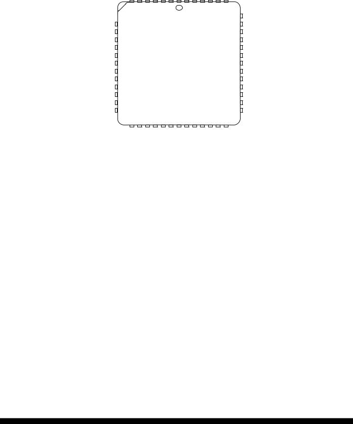
Figure 2 52-Pin PLCC Pin Assignments
MC68HC11A8 |
MOTOROLA |
MC68HC11A8TS/D |
5 |
|
1 |
|
|
|
VDD |
|
|
||||||
PA7/PAI/OC1 |
48 |
|
|||||||||||
PA6/OC2/OC1 |
2 |
47 |
PD5/SS |
|
|
|
|||||||
PA5/OC3/OC1 |
3 |
46 |
|
PD4/SCK |
|||||||||
PA4/OC4/OC1 |
4 |
45 |
|
PD3/MOSI |
|||||||||
PA3/OC5/OC1 |
5 |
44 |
|
PD2/MISO |
|||||||||
PA2/IC1 |
6 |
43 |
|
PD1/TxD |
|||||||||
PA1/IC2 |
7 |
42 |
|
PD0/RxD |
|||||||||
PA0/IC3 |
8 |
41 |
|
|
|
|
|
|
|
|
|||
|
IRQ |
||||||||||||
PB7/A15 |
9 |
40 |
|
|
|
|
|
|
|
||||
|
XIRQ |
||||||||||||
PB6/A14 |
10 |
39 |
|
|
|
|
|
|
|||||
|
RESET |
||||||||||||
PB5/A13 |
11 |
38 |
|
PC7/A7/D7 |
|||||||||
PB4/A12 |
12 |
37 |
|
PC6/A6/D6 |
|||||||||
PB3/A11 |
13 |
36 |
|
PC5/A5/D5 |
|||||||||
PB2/A10 |
14 |
35 |
|
PC4/A4/D4 |
|||||||||
PB1/A9 |
15 |
34 |
|
PC3/A3/D3 |
|||||||||
PB0/A8 |
16 |
33 |
|
PC2/A2/D2 |
|||||||||
PE0/AN0 |
17 |
32 |
|
PC1/A1/D1 |
|||||||||
PE1/AN1 |
18 |
31 |
|
PC0/A0/D0 |
|||||||||
PE2/AN2 |
19 |
30 |
|
XTAL |
|||||||||
PE3/AN3 |
20 |
29 |
|
EXTAL |
|||||||||
VRL |
21 |
28 |
|
|
|
|
|
||||||
|
STRB/ R/W |
||||||||||||
VRH |
22 |
27 |
|
E |
|||||||||
VSS |
23 |
26 |
|
STRA/AS |
|||||||||
MODB/VSTBY |
24 |
25 |
|
|
|
|
|||||||
|
MODA/LIR |
||||||||||||
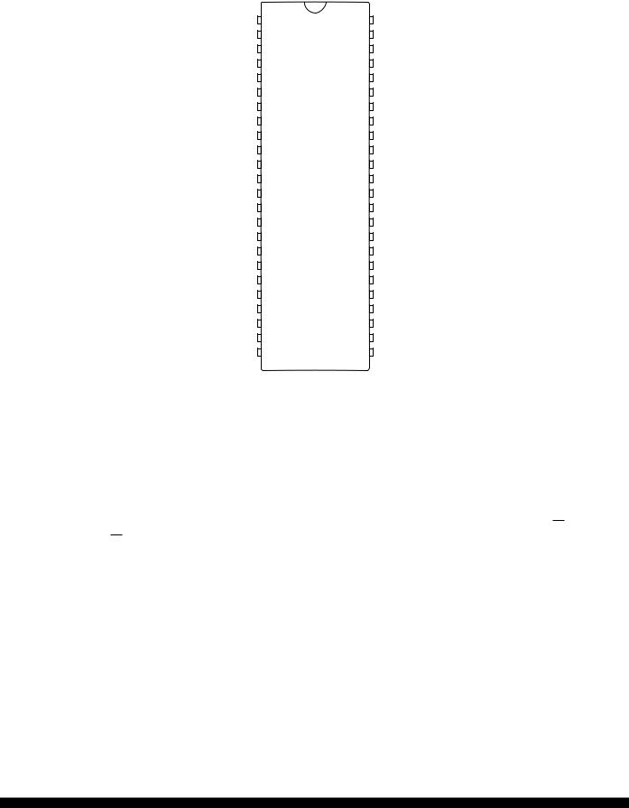
Figure 3 48-Pin DIP Pin Assignments
2 Operating Modes and Memory Maps
In single-chip operating mode, the MC68HC11A8 is a monolithic microcontroller without external address or data buses.
In expanded multiplexed operating mode, the MCU can access a 64 Kbyte address space. The space includes the same on-chip memory addresses used for single-chip mode plus external peripheral and memory devices. The expansion bus is made up of ports B and C and control signals AS and R/W. The address, R/W, and AS signals are active and valid for all bus cycles including accesses to internal memory locations. The following figure illustrates a recommended method of demultiplexing low-order addresses from data at port C.
MOTOROLA |
MC68HC11A8 |
6 |
MC68HC11A8TS/D |

PB7 |
|
|
|
|
|
|
|
|
|
|
|
|
|
|
|
|
|
|
|
|
|
|
|
|
A15 |
||||
|
|
|
|
|
|
|
|
|
|
|
|
|
|
|
|
|
|
|
|
|
|
|
|
||||||
PB6 |
|
|
|
|
|
|
|
|
|
|
|
|
|
|
|
|
|
|
|
|
|
|
|
|
A14 |
||||
|
|
|
|
|
|
|
|
|
|
|
|
|
|
|
|
|
|
|
|
|
|
|
|
||||||
PB5 |
|
|
|
|
|
|
|
|
|
|
|
|
|
|
|
|
|
|
|
|
|
|
|
|
A13 |
||||
|
|
|
|
|
|
|
|
|
|
|
|
|
|
|
|
|
|
|
|
|
|
|
|
||||||
PB4 |
|
|
|
|
|
|
|
|
|
|
|
|
|
|
|
|
|
|
|
|
|
|
|
|
A12 |
||||
|
|
|
|
|
|
|
|
|
|
|
|
|
|
|
|
|
|
|
|
|
|
|
|
||||||
PB3 |
|
|
|
|
|
|
|
|
|
|
|
|
|
|
|
|
|
|
|
|
|
|
|
|
A11 |
||||
|
|
|
|
|
|
|
|
|
|
|
|
|
|
|
|
|
|
|
|
|
|
|
|
||||||
PB2 |
|
|
|
|
|
|
|
|
|
|
|
|
|
|
|
|
|
|
|
|
|
|
|
|
A10 |
||||
|
|
|
|
|
|
|
|
|
|
|
|
|
|
|
|
|
|
|
|
|
|
|
|
||||||
PB1 |
|
|
|
|
|
|
|
|
|
|
|
|
|
|
|
|
|
|
|
|
|
|
|
|
A9 |
||||
|
|
|
|
|
|
|
|
|
|
|
|
|
|
|
|
|
|
|
|
|
|
|
|
||||||
PB0 |
|
|
|
|
|
|
|
|
|
|
|
|
|
|
|
|
|
|
|
|
|
|
|
|
A8 |
||||
|
|
|
|
|
|
|
|
|
MC54/74HC373 |
|
|
|
|
|
|
|
|
|
|
||||||||||
MC68HC11A8 |
|
|
|
|
|
|
|
|
|
|
|
|
|
|
|
|
|
|
|
|
|
|
|||||||
PC7 |
|
|
|
|
|
|
|
|
|
D1 |
Q1 |
|
|
|
|
|
|
|
|
|
|
A7 |
|||||||
|
|
|
|
|
|
|
|
|
|
|
|
|
|
|
|
|
|
|
|||||||||||
PC6 |
|
|
|
|
|
|
|
|
|
D2 |
Q2 |
|
|
|
|
|
|
|
|
|
|
A6 |
|||||||
|
|
|
|
|
|
|
|
|
|
|
|
|
|
|
|
|
|
|
|||||||||||
PC5 |
|
|
|
|
|
|
|
|
|
D3 |
Q3 |
|
|
|
|
|
|
|
|
|
|
A5 |
|||||||
|
|
|
|
|
|
|
|
|
|
|
|
|
|
|
|
|
|
|
|||||||||||
PC4 |
|
|
|
|
|
|
|
|
|
D4 |
Q4 |
|
|
|
|
|
|
|
|
|
|
A4 |
|||||||
|
|
|
|
|
|
|
|
|
|
|
|
|
|
|
|
|
|
|
|||||||||||
PC3 |
|
|
|
|
|
|
|
|
|
D5 |
Q5 |
|
|
|
|
|
|
|
|
|
|
A3 |
|||||||
|
|
|
|
|
|
|
|
|
|
|
|
|
|
|
|
|
|
|
|||||||||||
PC2 |
|
|
|
|
|
|
|
|
|
D6 |
Q6 |
|
|
|
|
|
|
|
|
|
|
A2 |
|||||||
|
|
|
|
|
|
|
|
|
|
|
|
|
|
|
|
|
|
|
|||||||||||
PC1 |
|
|
|
|
|
|
|
|
|
D7 |
Q7 |
|
|
|
|
|
|
|
|
|
|
A1 |
|||||||
|
|
|
|
|
|
|
|
|
|
|
|
|
|
|
|
|
|
|
|||||||||||
PC0 |
|
|
|
|
|
|
|
|
|
D8 |
Q8 |
|
|
|
|
|
|
|
|
|
|
A0 |
|||||||
|
|
|
|
|
|
|
|
|
|
|
|
|
|
|
|
|
|
|
|||||||||||
AS |
|
|
|
|
|
|
|
|
|
LE |
|
|
|
|
|
|
|
|
|
|
|
|
|
|
|
|
|||
|
|
|
|
|
|
|
|
|
OE |
|
|
|
|
|
|
|
|
|
|
|
|
|
|||||||
|
|
|
|
|
|
|
|
|
|
|
|
|
|
|
|
|
|
|
|
|
|
||||||||
|
|
|
|
|
|
|
|
|
|
|
|
|
|
|
|
|
|
|
|
|
|
|
|
|
|
|
|
|
|
|
|
|
|
|
|
|
|
|
|
|
|
|
|
|
|
|
|
|
|
|
|
|
|
|
|
|
|
|
|
|
|
|
|
|
|
|
|
|
|
|
|
|
|
|
|
|
|
|
|
|
|
|
|
|
|
|
|
|
|
|
|
|
|
|
|
|
|
|
|
|
|
|
|
|
|
|
|
|
|
|
|
|
|
|
|
|
|
|
|
|
|
|
|
|
|
|
|
|
|
|
|
|
|
|
|
|
|
|
|
|
|
|
|
|
|
|
|
|
|
R/W |
|
|
|
|
|
|
|
|
|
|
|
|
|
|
|
|
|
|
|
|
|
|
|
|
|
|
|
|
|
|
E |
|
|
|
|
|
|
|
|
|
|
|
|
|
|
|
|
|
|
|
|
|
|
|
|
|
WE |
|
|
|
|
|
|
|
|
|
|
|
|
|
|
|
|
|
|
|
|
|
|
|
|
|
|
|
|||||
|
|
|
|
|
|
|
|
|
|
|
|
|
|
|
|
|
|
|
|
|
|
|
|
|
D7 |
||||
|
|
|
|
|
|
|
|
|
|
|
|
|
|
|
|
|
|
|
|
|
|
|
|
|
|||||
|
|
|
|
|
|
|
|
|
|
|
|
|
|
|
|
|
|
|
|
|
|
|
|
|
|||||
|
|
|
|
|
|
|
|
|
|
|
|
|
|
|
|
|
|
|
|
|
|
|
|
|
|
|
|||
|
|
|
|
|
|
|
|
|
|
|
|
|
|
|
|
|
|
|
|
|
|
|
|
|
|
|
|||
|
|
|
|
|
|
|
|
|
|
|
|
|
|
|
|
|
|
|
|
|
|
|
|
|
|
|
D6 |
||
|
|
|
|
|
|
|
|
|
|
|
|
|
|
|
|
|
|
|
|
|
|
|
|
|
|
|
|||
|
|
|
|
|
|
|
|
|
|
|
|
|
|
|
|
|
|
|
|
|
|
|
|
|
|
|
D5 |
||
|
|
|
|
|
|
|
|
|
|
|
|
|
|
|
|
|
|
|
|
|
|
|
|
|
|
|
|||
|
|
|
|
|
|
|
|
|
|
|
|
|
|
|
|
|
|
|
|
|
|
|
|
|
|
|
D4 |
||
|
|
|
|
|
|
|
|
|
|
|
|
|
|
|
|
|
|
|
|
|
|
|
|
|
|
|
|||
|
|
|
|
|
|
|
|
|
|
|
|
|
|
|
|
|
|
|
|
|
|
|
|
|
|
|
D3 |
||
|
|
|
|
|
|
|
|
|
|
|
|
|
|
|
|
|
|
|
|
|
|
|
|
|
|
|
|||
|
|
|
|
|
|
|
|
|
|
|
|
|
|
|
|
|
|
|
|
|
|
|
|
|
|
|
D2 |
||
|
|
|
|
|
|
|
|
|
|
|
|
|
|
|
|
|
|
|
|
|
|
|
|
|
|
|
|||
|
|
|
|
|
|
|
|
|
|
|
|
|
|
|
|
|
|
|
|
|
|
|
|
|
|
|
D1 |
||
|
|
|
|
|
|
|
|
|
|
|
|
|
|
|
|
|
|
|
|
|
|
|
|
|
|
|
|||
|
|
|
|
|
|
|
|
|
|
|
|
|
|
|
|
|
|
|
|
|
|
|
|
|
|
|
D0 |
||
|
|
|
|
|
|
|
|
|
|
|
|
|
|
|
|
|
|
|
|
|
|
|
|
|
|
|
|||
Figure 4 Address/Data Demultiplexing
Special bootstrap mode allows special purpose programs to be entered into internal RAM. The bootloader program uses the SCI to read a 256-byte program into on-chip RAM at $0000 through $00FF. After receiving the character for address $00FF, control passes to the loaded program at $0000.
Special test mode is used primarily for factory testing.
2.1 Memory Maps
Memory locations are the same for expanded multiplexed and single-chip modes. The on-board 256byte RAM is initially located at $0000 after reset. The 64-byte register block originates at $1000 after reset. RAM and/or the register block can be placed at any other 4K boundary ($x000) after reset by writing an appropriate value to the INIT register. The 512-byte EEPROM is located at $B600 through $B7FF after reset if it is enabled. The 8 Kbyte ROM is located at $E000 through $FFFF if it is enabled.
Hardware priority is built into the memory remapping. Registers have priority over RAM, and RAM has priority over ROM. The higher priority resource covers the lower, making the underlying locations inaccessible.
In special bootstrap mode, a bootloader ROM is enabled at locations $BF40 through $BFFF.
In special test and special bootstrap modes, reset and interrupt vectors are located at $BFC0 through $BFFF.
MC68HC11A8 |
MOTOROLA |
MC68HC11A8TS/D |
7 |
$0000 |
|
|
0000 |
256 BYTES RAM |
|
|
|
|
|
|
|
|
|
|
EXT |
|
EXT |
(CAN BE REMAPPED TO ANY |
||
|
|
4K PAGE BY THE INIT REGISTER) |
||||
|
|
|
00FF |
|
|
|
$1000 |
|
|
1000 |
64 BYTE REGISTER BLOCK |
|
|
|
|
|
|
|
||
|
|
|
|
(CAN BE REMAPPED TO ANY |
||
|
|
|
103F |
4K PAGE BY THE INIT REGISTER) |
||
|
|
|
|
|
|
|
|
EXT |
|
EXT |
|
|
|
|
|
|
B600 |
512 BYTES EEPROM |
|
|
|
|
|
|
|
||
$B600 |
|
|
|
|
|
|
|
|
|
B7FF |
|
|
|
|
|
|
BF40 |
BOOT |
BFC0 |
SPECIAL |
|
|
|
EXT |
ROM |
|
MODE |
|
EXT |
|
|
|
INTERRUPT |
|
|
|
BFFF |
|
BFFF |
VECTORS |
|
|
|
|
|
|||
|
|
|
E000 |
8K ROM |
|
|
|
|
|
|
|
|
|
$E000 |
|
|
|
|
FFC0 |
|
|
|
|
|
|
NORMAL |
|
|
|
|
|
|
|
|
|
|
|
|
|
|
MODE |
|
|
|
|
|
|
INTERRUPT |
$FFFF |
|
|
FFFF |
|
FFFF |
VECTORS |
|
|
|
|
|||
SINGLE |
EXPANDED |
SPECIAL |
SPECIAL |
|
|
|
CHIP |
MUX |
BOOTSTRAP |
TEST |
|
|
|
Figure 5 Memory Map
MOTOROLA |
MC68HC11A8 |
8 |
MC68HC11A8TS/D |
Table 3 MC68HC11A8 Register and Control Bit Assignments (Sheet 1 of 2)
(The register block can be remapped to any 4K boundary.)
|
Bit 7 |
6 |
5 |
4 |
3 |
2 |
1 |
Bit 0 |
|
$1000 |
PA7 |
PA6 |
PA5 |
PA4 |
PA3 |
PA2 |
PA1 |
PA0 |
PORTA |
$1001 |
|
|
|
|
|
|
|
|
Reserved |
|
|
|
|
|
|
|
|
||
|
|
|
|
|
|
|
|
|
|
$1002 |
STAF |
STAI |
CWOM |
HNDS |
OIN |
PLS |
EGA |
INVB |
PIOC |
|
|
|
|
|
|
|
|
|
|
$1003 |
PC7 |
PC6 |
PC5 |
PC4 |
PC3 |
PC2 |
PC1 |
PC0 |
PORTC |
|
|
|
|
|
|
|
|
|
|
$1004 |
PB7 |
PB6 |
PB5 |
PB4 |
PB3 |
PB2 |
PB1 |
PB0 |
PORTB |
|
|
|
|
|
|
|
|
|
|
$1005 |
PCL7 |
PCL6 |
PCL5 |
PCL4 |
PCL3 |
PCL2 |
PCL1 |
PCL0 |
PORTCL |
$1006 |
|
|
|
|
|
|
|
|
Reserved |
|
|
|
|
|
|
|
|
||
|
|
|
|
|
|
|
|
|
|
$1007 |
DDC7 |
DDC6 |
DDC5 |
DDC4 |
DDC3 |
DDC2 |
DDC1 |
DDC0 |
DDRC |
|
|
|
|
|
|
|
|
|
|
$1008 |
0 |
0 |
PD5 |
PD4 |
PD3 |
PD2 |
PD1 |
PD0 |
PORTD |
|
|
|
|
|
|
|
|
|
|
$1009 |
0 |
0 |
DDD5 |
DDD4 |
DDD3 |
DDD2 |
DDD1 |
DDD0 |
DDRD |
|
|
|
|
|
|
|
|
|
|
$100A |
PE7 |
PE6 |
PE5 |
PE4 |
PE3 |
PE2 |
PE1 |
PE0 |
PORTE |
|
|
|
|
|
|
|
|
|
|
$100B |
FOC1 |
FOC2 |
FOC3 |
FOC4 |
FOC5 |
0 |
0 |
0 |
CFORC |
|
|
|
|
|
|
|
|
|
|
$100C |
OC1M7 |
OC1M6 |
OC1M5 |
OC1M4 |
OC1M3 |
0 |
0 |
0 |
OC1M |
|
|
|
|
|
|
|
|
|
|
$100D |
OC1D7 |
OC1D6 |
OC1D5 |
OC1D4 |
OC1D3 |
0 |
0 |
0 |
OC1D |
|
|
|
|
|
|
|
|
|
|
$100E |
Bit 15 |
14 |
13 |
12 |
11 |
10 |
9 |
Bit 8 |
TCNT (High) |
|
|
|
|
|
|
|
|
|
|
$100F |
Bit 7 |
6 |
5 |
4 |
3 |
2 |
1 |
Bit 0 |
TCNT (Low) |
|
|
|
|
|
|
|
|
|
|
$1010 |
Bit 15 |
14 |
13 |
12 |
11 |
10 |
9 |
Bit 8 |
TIC1 (High) |
|
|
|
|
|
|
|
|
|
|
$1011 |
Bit 7 |
6 |
5 |
4 |
3 |
2 |
1 |
Bit 0 |
TIC1 (Low) |
|
|
|
|
|
|
|
|
|
|
$1012 |
Bit 15 |
14 |
13 |
12 |
11 |
10 |
9 |
Bit 8 |
TIC2 (High) |
|
|
|
|
|
|
|
|
|
|
$1013 |
Bit 7 |
6 |
5 |
4 |
3 |
2 |
1 |
Bit 0 |
TIC2 (Low) |
|
|
|
|
|
|
|
|
|
|
$1014 |
Bit 15 |
14 |
13 |
12 |
11 |
10 |
9 |
Bit 8 |
TIC3 (High) |
|
|
|
|
|
|
|
|
|
|
$1015 |
Bit 7 |
6 |
5 |
4 |
3 |
2 |
1 |
Bit 0 |
TIC3 (Low) |
|
|
|
|
|
|
|
|
|
|
$1016 |
Bit 15 |
14 |
13 |
12 |
11 |
10 |
9 |
Bit 8 |
TOC1(High) |
|
|
|
|
|
|
|
|
|
|
$1017 |
Bit 7 |
6 |
5 |
4 |
3 |
2 |
1 |
Bit 0 |
TOC1 (Low) |
|
|
|
|
|
|
|
|
|
|
$1018 |
Bit 15 |
14 |
13 |
12 |
11 |
10 |
9 |
Bit 8 |
TOC2 (High) |
|
|
|
|
|
|
|
|
|
|
$1019 |
Bit 7 |
6 |
5 |
4 |
3 |
2 |
1 |
Bit 0 |
TOC2 (Low) |
|
|
|
|
|
|
|
|
|
|
$101A |
Bit 15 |
14 |
13 |
12 |
11 |
10 |
9 |
Bit 8 |
TOC3 (High) |
|
|
|
|
|
|
|
|
|
|
$101B |
Bit 7 |
6 |
5 |
4 |
3 |
2 |
1 |
Bit 0 |
TOC3 (Low) |
|
|
|
|
|
|
|
|
|
|
$101C |
Bit 15 |
14 |
13 |
12 |
11 |
10 |
9 |
Bit 8 |
TOC4 (High) |
|
|
|
|
|
|
|
|
|
|
$101D |
Bit 7 |
6 |
5 |
4 |
3 |
2 |
1 |
Bit 0 |
TOC4 (Low) |
|
|
|
|
|
|
|
|
|
|
$101E |
Bit 15 |
14 |
13 |
12 |
11 |
10 |
9 |
Bit 8 |
TOC5 (High) |
|
|
|
|
|
|
|
|
|
|
$101F |
Bit 7 |
6 |
5 |
4 |
3 |
2 |
1 |
Bit 0 |
TOC5 (Low) |
|
|
|
|
|
|
|
|
|
|
$1020 |
OM2 |
OL2 |
OM3 |
OL3 |
OM4 |
OL4 |
OM5 |
OL5 |
TCTL1 |
|
|
|
|
|
|
|
|
|
|
$1021 |
0 |
0 |
EDG1B |
EDG1A |
EDG2B |
EDG2A |
EDG3B |
EDG3A |
TCTL2 |
|
|
|
|
|
|
|
|
|
|
$1022 |
OC1I |
OC2I |
OC3I |
OC4I |
OC5I |
IC1I |
IC2I |
IC3I |
TMSK1 |
|
|
|
|
|
|
|
|
|
|
$1023 |
OC1F |
OC2F |
OC3F |
OC4F |
OC5F |
IC1F |
IC2F |
IC3F |
TFLG1 |
|
|
|
|
|
|
|
|
|
|
$1024 |
TOI |
RTII |
PAOVI |
PAII |
0 |
0 |
PR1 |
PR0 |
TMSK2 |
|
|
|
|
|
|
|
|
|
|
$1025 |
TOF |
RTIF |
PAOVF |
PAIF |
0 |
0 |
0 |
0 |
TFLG2 |
|
|
|
|
|
|
|
|
|
|
|
|
|
|
|
|
|
|
|
|
|
|
|
|
|
|
|
|
|
|
MC68HC11A8 |
MOTOROLA |
MC68HC11A8TS/D |
9 |

Table 3 MC68HC11A8 Register and Control Bit Assignments (Sheet 2 of 2)
(The register block can be remapped to any 4K boundary.)
|
Bit 7 |
6 |
5 |
4 |
3 |
2 |
1 |
Bit 0 |
|
$1026 |
DDRA7 |
PAEN |
PAMOD |
PEDGE |
0 |
0 |
RTR1 |
RTR0 |
PACTL |
|
|
|
|
|
|
|
|
|
|
$1027 |
Bit 7 |
6 |
5 |
4 |
3 |
2 |
1 |
Bit 0 |
PACNT |
|
|
|
|
|
|
|
|
|
|
$1028 |
SPIE |
SPE |
DWOM |
MSTR |
CPOL |
CPHA |
SPR1 |
SPR0 |
SPCR |
|
|
|
|
|
|
|
|
|
|
$1029 |
SPIF |
WCOL |
0 |
MODF |
0 |
0 |
0 |
0 |
SPSR |
|
|
|
|
|
|
|
|
|
|
$102A |
Bit 7 |
6 |
5 |
4 |
3 |
2 |
1 |
Bit 0 |
SPDR |
|
|
|
|
|
|
|
|
|
|
$102B |
TCLR |
0 |
SCP1 |
SCP0 |
RCKB |
SCR2 |
SCR1 |
SCR0 |
BAUD |
|
|
|
|
|
|
|
|
|
|
$102C |
R8 |
T8 |
0 |
M |
WAKE |
0 |
0 |
0 |
SCCR1 |
|
|
|
|
|
|
|
|
|
|
$102D |
TIE |
TCIE |
RIE |
ILIE |
TE |
RE |
RWU |
SBK |
SCCR2 |
|
|
|
|
|
|
|
|
|
|
$102E |
TDRE |
TC |
RDRF |
IDLE |
OR |
NF |
FE |
0 |
SCSR |
|
|
|
|
|
|
|
|
|
|
$102F |
R7/T7 |
R6/T6 |
R5/T5 |
R4/T4 |
R3/T3 |
R2/T2 |
R1/T1 |
R0/T0 |
SCDR |
|
|
|
|
|
|
|
|
|
|
$1030 |
CCF |
0 |
SCAN |
MULT |
CD |
CC |
CB |
CA |
ADCTL |
|
|
|
|
|
|
|
|
|
|
$1031 |
Bit 7 |
6 |
5 |
4 |
3 |
2 |
1 |
Bit 0 |
ADR1 |
|
|
|
|
|
|
|
|
|
|
$1032 |
Bit 7 |
6 |
5 |
4 |
3 |
2 |
1 |
Bit 0 |
ADR2 |
|
|
|
|
|
|
|
|
|
|
$1033 |
Bit 7 |
6 |
5 |
4 |
3 |
2 |
1 |
Bit 0 |
ADR3 |
|
|
|
|
|
|
|
|
|
|
$1034 |
Bit 7 |
6 |
5 |
4 |
3 |
2 |
1 |
Bit 0 |
ADR4 |
$1035 |
|
|
|
|
|
|
|
|
Reserved |
|
|
|
|
|
|
|
|
||
$1038 |
|
|
|
|
|
|
|
|
Reserved |
|
|
|
|
|
|
|
|
||
|
|
|
|
|
|
|
|
|
|
$1039 |
ADPU |
CSEL |
IRQE |
DLY |
CME |
0 |
CR1 |
CR0 |
OPTION |
|
|
|
|
|
|
|
|
|
|
$103A |
Bit 7 |
6 |
5 |
4 |
3 |
2 |
1 |
Bit 0 |
COPRST |
|
|
|
|
|
|
|
|
|
|
$103B |
ODD |
EVEN |
0 |
BYTE |
ROW |
ERASE |
EELAT |
EEPGM |
PPROG |
|
|
|
|
|
|
|
|
|
|
$103C |
RBOOT |
SMOD |
MDA |
IRV |
PSEL3 |
PSEL2 |
PSEL1 |
PSEL0 |
HPRIO |
|
|
|
|
|
|
|
|
|
|
$103D |
RAM3 |
RAM2 |
RAM1 |
RAM0 |
REG3 |
REG2 |
REG1 |
REG0 |
INIT |
|
|
|
|
|
|
|
|
|
|
$103E |
TILOP |
0 |
OCCR |
CBYP |
DISR |
FCM |
FCOP |
TCON |
TEST1 |
|
|
|
|
|
|
|
|
|
|
$103F |
0 |
0 |
0 |
0 |
NOSEC |
NOCOP |
ROMON |
EEON |
CONFIG |
|
|
|
|
|
|
|
|
|
|
MOTOROLA |
MC68HC11A8 |
10 |
MC68HC11A8TS/D |
HPRIO — Highest Priority I-Bit Interrupt and Miscellaneous |
|
|
$103C |
|||||||
|
Bit 7 |
6 |
5 |
|
4 |
3 |
|
2 |
1 |
Bit 0 |
|
|
|
|
|
|
|
|
|
|
|
|
RBOOT |
SMOD |
MDA |
|
IRV |
PSEL3 |
|
PSEL2 |
PSEL1 |
PSEL0 |
|
|
|
|
|
|
|
|
|
|
|
RESET: |
— |
— |
— |
— |
|
0 |
|
1 |
0 |
1 |
RBOOT, SMOD, and MDA reset depend on conditions at reset and can only be written in special modes (SMOD = 1).
RBOOT — Read Bootstrap ROM
0 = Bootloader ROM disabled and not in map
1 = Bootloader ROM enabled and in map at $BF40–$BFFF
SMOD —Special Mode Select
MDA — Mode Select A
Inputs |
|
Mode |
|
Latched at Reset |
|
||
|
|
|
|
|
|
|
|
MODB |
MODA |
|
RBOOT |
|
SMOD |
|
MDA |
|
|
|
|
|
|
|
|
1 |
0 |
Single Chip |
0 |
|
0 |
|
0 |
|
|
|
|
|
|
|
|
1 |
1 |
Expanded Multiplexed |
0 |
|
0 |
|
1 |
|
|
|
|
|
|
|
|
0 |
0 |
Special Bootstrap |
1 |
|
1 |
|
0 |
|
|
|
|
|
|
|
|
0 |
1 |
Special Test |
0 |
|
1 |
|
1 |
|
|
|
|
|
|
|
|
IRV — Internal Read Visibility
0 = No internal read visibility on external bus
1 = Data from internal reads is driven out through the external data bus
PSEL3–PSEL0 — Priority Select Bits 3 through 0
Refer to 3 Resets and Interrupts.
INIT — RAM and I/O Mapping |
|
|
|
|
|
$103D |
|||
|
Bit 7 |
6 |
|
5 |
4 |
3 |
2 |
1 |
Bit 0 |
|
|
|
|
|
|
|
|
|
|
|
RAM3 |
RAM2 |
|
RAM1 |
RAM0 |
REG3 |
REG2 |
REG1 |
REG0 |
|
|
|
|
|
|
|
|
|
|
RESET: |
0 |
0 |
|
0 |
0 |
0 |
0 |
0 |
1 |
RAM[3:0] —256-Byte Internal RAM Map Position
RAM[3:0] determine the upper four bits of the RAM address, positioning RAM at the selected 4K boundary.
REG[3:0] —64-Byte Register Block Map Position
REG[3:0] determine the upper four bits of the register address, positioning registers at the selected 4K boundary. Register can be written only once in the first 64 cycles out of reset in normal modes, or any time in special modes.
MC68HC11A8 |
MOTOROLA |
MC68HC11A8TS/D |
11 |

TEST1 — Factory Test |
|
|
|
|
|
|
$103E |
||
|
Bit 7 |
6 |
5 |
4 |
3 |
2 |
1 |
Bit 0 |
|
|
|
|
|
|
|
|
|
|
|
|
TILOP |
|
0 |
OCCR |
CBYP |
DISR |
FCM |
FCOP |
TCON |
|
|
|
|
|
|
|
|
|
|
RESET: |
0 |
|
0 |
0 |
0 |
— |
0 |
0 |
0 |
Test Modes Only
TILOP — Test Illegal Opcode
OCCR — Output Condition Code Register to Timer Port
CBYP — Timer Divider Chain Bypass
DISR — Disable Resets from COP and Clock Monitor
DISR is forced to one out of reset in special test and bootstrap modes.
FCM — Force Clock Monitor Failure
FCOP — Force COP Watchdog Failure
TCON — Test Configuration Register
CONFIG — COP, ROM, EEPROM Enables |
|
|
|
|
$103F |
||||
|
Bit 7 |
6 |
5 |
|
4 |
3 |
2 |
1 |
Bit 0 |
|
|
|
|
|
|
|
|
|
|
|
0 |
0 |
0 |
|
0 |
NOSEC |
NOCOP |
ROMON |
EEON |
|
|
|
|
|
|
|
|
|
|
RESET: |
0 |
0 |
0 |
|
0 |
— |
— |
— |
— |
NOTE
The bits of this register are implemented with EEPROM cells. Programming and erasing follow normal EEPROM procedures. The erased state of CONFIG is $0F. A new value is not readable until after a subsequent reset sequence. CONFIG can only be programmed or erased in special modes.
NOSEC — EEPROM Security Disable
Refer to 4 Electrically Erasable Programmable Read-Only Memory (EEPROM).
NOCOP — COP System Disable
Refer to 3 Resets and Interrupts.
ROMON — ROM Enable
In single-chip mode, ROMON is forced to one out of reset. 0 = 8K ROM removed from the memory map
1 = 8K ROM present in the memory map
EEON — EEPROM Enable
0 = EEPROM is removed from the memory map
1 = EEPROM is present in the memory map
MOTOROLA |
MC68HC11A8 |
12 |
MC68HC11A8TS/D |

3 Resets and Interrupts
The MC68HC11A8 has three reset vectors and 18 interrupt vectors. The reset vectors are as follows:
•RESET, or Power-On
•COP Clock Monitor Fail
•COP Failure
The eight interrupt vectors service 23 interrupt sources (three non-maskable, 20 maskable). The three non-maskable interrupt vectors are as follows:
•Illegal Opcode Trap
•Software Interrupt
•XIRQ Pin (Pseudo Non-Maskable Interrupt)
The 20 maskable interrupt sources are subject to masking by a global interrupt mask, the I bit in the condition code register (CCR). In addition to the global I bit, all of these sources except the external interrupt (IRQ) pin are controlled by local enable bits in control registers. Most interrupt sources in the M68HC11 have separate interrupt vectors. For this reason, there is usually no need for software to poll control registers to determine the cause of an interrupt. The maskable interrupt sources respond to a fixed priority relationship, except that any one source can be dynamically elevated to the highest priority position of any maskable source. Refer to the table of interrupt and reset vector assignments.
On-chip peripheral systems generate maskable interrupts that are recognized only if the I bit in the CCR is clear. Maskable interrupts are prioritized according to a default arrangement, but any one source can be elevated to the highest maskable priority position by the HPRIO register. The HPRIO register can be written at any time, provided the I bit in the CCR is set.
For some interrupt sources, such as the parallel I/O and SCI interrupts, the flags are automatically cleared during the course of responding to the interrupt requests. For example, the RDRF flag in the SCI system is cleared by the automatic clearing mechanism, which consists of a read of the SCI status register while RDRF is set, followed by a read of the SCI data register. The normal response to an RDRF interrupt request is to read the SCI status register to check for receive errors, then to read the received data from the SCI data register. These two steps satisfy the automatic clearing mechanism without requiring any special instructions.
The real-time interrupt (RTI) function generates hardware interrupts at a fixed periodic rate. These hardware interrupts provide a time reference signal for routines that measure real time. The routine notes the number of times a particular interrupt has occurred and multiplies that number by the predetermined subroutine execution time.
There are four RTI signal rates available in the MC68HC11A8. The MCU oscillator frequency and the value of two software-accessible control bits, RTR1 and RTR0, in the pulse accumulator control register (PACTL) determine these signal rates. Refer to 8 Main Timer for more information about PACTL.
MC68HC11A8 |
MOTOROLA |
MC68HC11A8TS/D |
13 |

Table 4 Interrupt and Reset Vector Assignments
Vector Address |
|
|
|
Interrupt Source |
CCR Mask |
Local Mask |
|
|
|
|
|
|
|||
FFC0, C1 – FFD4, D5 |
|
Reserved |
— |
— |
|||
|
|
|
|
|
|
||
FFD6, |
D7 |
|
SCI Serial System |
I Bit |
|
||
|
|
|
|
|
|
|
|
|
|
|
|
• SCI Transmit Complete |
|
TCIE |
|
|
|
|
|
|
|
|
|
|
|
|
|
• SCI Transmit Data Register Empty |
|
TIE |
|
|
|
|
|
|
|
|
|
|
|
|
|
• SCI Idle Line Detect |
|
ILIE |
|
|
|
|
|
|
|
|
|
|
|
|
|
• SCI Receiver Overrun |
|
RIE |
|
|
|
|
|
|
|
|
|
|
|
|
|
• SCI Receive Data Register Full |
|
RIE |
|
|
|
|
|
|
|
||
FFD8, |
D9 |
|
SPI Serial Transfer Complete |
I Bit |
SPIE |
||
|
|
|
|
|
|
||
FFDA, |
DB |
|
Pulse Accumulator Input Edge |
I Bit |
PAII |
||
|
|
|
|
|
|||
FFDC, DD |
|
Pulse Accumulator Overflow |
I Bit |
PAOVI |
|||
|
|
|
|
|
|||
FFDE, DF |
|
Timer Overflow |
I Bit |
TOI |
|||
|
|
|
|
|
|
||
FFE0, |
E1 |
|
Timer Input Capture 4/Output Compare 5 |
I Bit |
I4O5I |
||
|
|
|
|
|
|
||
FFE3, |
E2 |
|
Timer Output Compare 4 |
I Bit |
OC4I |
||
|
|
|
|
|
|
||
FFE4, |
E5 |
|
Timer Output Compare 3 |
I Bit |
OC3I |
||
|
|
|
|
|
|
||
FFE6, |
E7 |
|
Timer Output Compare 2 |
I Bit |
OC2I |
||
|
|
|
|
|
|
||
FFE8, |
E9 |
|
Timer Output Compare 1 |
I Bit |
OC1I |
||
|
|
|
|
|
|
||
FFEA, |
EB |
|
Timer Input Capture 3 |
I Bit |
IC3 |
||
|
|
|
|
|
|||
FFEC, ED |
|
Timer Input Capture 2 |
I Bit |
IC2I |
|||
|
|
|
|
|
|||
FFEE, EF |
|
Timer Input Capture 1 |
I Bit |
IC1I |
|||
|
|
|
|
|
|
||
FFF0, |
F1 |
|
Real-Time Interrupt |
I Bit |
RTII |
||
|
|
|
|
|
|
||
FFF2, |
F3 |
|
Parallel I/O Handshake |
I Bit |
STAI |
||
|
|
|
|
|
|
|
|
|
|
|
|
|
|
|
None |
|
|
|
IRQ |
|
|||
|
|
|
|
|
|
|
|
FFF4, |
F5 |
|
|
|
Pin |
X Bit |
None |
XIRQ |
|||||||
|
|
|
|
|
|
||
FFF6, |
F7 |
|
Software Interrupt |
None |
None |
||
|
|
|
|
|
|
||
FFF8, |
F9 |
|
Illegal Opcode Trap |
None |
None |
||
|
|
|
|
|
|||
FFFA, FB |
|
COP Failure |
None |
NOCOP |
|||
|
|
|
|
|
|||
FFFC, FD |
|
COP Clock Monitor Fail |
None |
CME |
|||
|
|
|
|
|
|||
FFFE, FF |
|
RESET |
None |
None |
|||
|
|
|
|
|
|
|
|
OPTION —System Configuration Options |
|
|
|
|
$1039 |
||||
|
Bit 7 |
6 |
5 |
|
4 |
3 |
2 |
1 |
Bit 0 |
|
|
|
|
|
|
|
|
|
|
|
ADPU |
CSEL |
IRQE* |
|
DLY* |
CME |
0 |
CR1* |
CR0* |
|
|
|
|
|
|
|
|
|
|
RESET: |
0 |
0 |
0 |
|
1 |
0 |
0 |
0 |
0 |
*Can be written only once in first 64 cycles out of reset in normal modes, or any time in special modes.
ADPU —A/D Converter Power-up
Refer to 10 Analog-to-Digital Converter.
CSEL —Clock Select
Refer to 10 Analog-to-Digital Converter.
IRQE — IRQ Select Edge-Sensitive Only 0 = Low logic level recognition
1 = Falling edge recognition
MOTOROLA |
MC68HC11A8 |
14 |
MC68HC11A8TS/D |
Loading...