


Motorola MC68HC705B5CFN, MC68HC705B5FN, MC68HC705B5MFN, MC68HC705B5VFN, MC68HC705B32FU Datasheet
...MC68HC05B6
MC68HC05B6/D
Rev. 3
HC05
DATA TECHNICAL
MC68HC05B4
MC68HC705B5
MC68HC05B6
MC68HC05B8
MC68HC05B16
MC68HC705B16
MC68HC05B32
MC68HC705B32
!MOTOROLA
TECHNICAL DATA

INTRODUCTION
MODES OF OPERATION AND PIN DESCRIPTIONS
MEMORY AND REGISTERS
INPUT/OUTPUT PORTS
PROGRAMMABLE TIMER
SERIAL COMMUNICATIONS INTERFACE
PULSE LENGTH D/A CONVERTERS
ANALOG TO DIGITAL CONVERTER
RESETS AND INTERRUPTS
CPU CORE AND INSTRUCTION SET
ELECTRICAL SPECIFICATIONS
MECHANICAL DATA
ORDERING INFORMATION
APPENDICES
HIGH SPEED OPERATION
1
2
3
4
5
6
7
8
9
10
11
12
13
14
15

1
2
3
4
5
6
7
8
9
10
11
12
13
14
15
INTRODUCTION
MODES OF OPERATION AND PIN DESCRIPTIONS
MEMORY AND REGISTERS
INPUT/OUTPUT PORTS
PROGRAMMABLE TIMER
SERIAL COMMUNICATIONS INTERFACE
PULSE LENGTH D/A CONVERTERS
ANALOG TO DIGITAL CONVERTER
RESETS AND INTERRUPTS
CPU CORE AND INSTRUCTION SET
ELECTRICAL SPECIFICATIONS
MECHANICAL DATA
ORDERING INFORMATION
MC68HC05B4
HIGH SPEED OPERATION

MC68HC05B6
High-density Complementary
Metal Oxide Semiconductor
(HCMOS) Microcomputer Unit
All Trade Marks recognised. This document contains information on new products. Specifications and information herein are subject to change without notice.
All products are sold on Motorola’s Terms & Conditions of Supply. In ordering a product covered by this document the Customer agrees to be bound by those Terms & Conditions and nothing contained in this document constitutes or forms part of a contract (with the exception of the contents of this Notice). A copy of Motorola’s Terms & Conditions of Supply is available on request.
Motorola reserves the right to make changes without further notice to any products herein. Motorola makes no warranty, representation or guarantee regarding the suitability of its products for any particular purpose, nor does Motorola assume any liability arising out of the application or use of any product or circuit, and specifically disclaims any and all liability, including without limitation consequential or incidental damages. “Typical” parameters can and do vary in different applications. All operating parameters, including “Typicals”, must be validated for each customer application by customer’s technical experts. Motorola does not convey any license under its patent rights nor the rights of others. Motorola products are not designed, intended, or authorized for use as components in systems intended for surgical implant into the body, or other applications intended to support or sustain life, or for any other application in which the failure of the Motorola product could create a situation where personal injury or death may occur. Should Buyer purchase or use Motorola products for any such unintended or unauthorized application, Buyer shall indemnify and hold Motorola and its officers, employees, subsidiaries, affiliates, and distributors harmless against all claims, costs, damages, and expenses, and reasonable attorney fees arising out of, directly or indirectly, any claim of personal injury or death associated with such unintended or unauthorized use, even if such claim alleges that Motorola was negligent regarding the design or manufacture of the part. Motorola and !are registered trademarks of Motorola, Inc. Motorola, Inc. is an Equal Opportunity/Affirmative Action Employer.
The Customer should ensure that it has the most up to date version of the document by contacting its local Motorola office. This document supersedes any earlier documentation relating to the products referred to herein. The information contained in this document is current at the date of publication. It may subsequently be updated, revised or withdrawn.
© MOTOROLA LTD., 1995

CAUTION
This document includes descriptions of the various self-check and bootstrap mechanisms that are currently implemented as firmware in the non-user ROM areas of the MC68HC05B6 and related devices.
As these firmware routines are intended primarily to help Motorola’s engineers test the devices, they may be changed or removed at any time.
For this reason, Motorola recommends that the self-check and bootstrap routines are not called from from the user software. Customers who do call these routines from the user software do so at their own risk.
TABLE OF CONTENTS
Paragraph |
Title |
Page |
Number |
Number |
1 INTRODUCTION
1.1 |
Features................................................................................................................ |
1-2 |
1.2 |
Mask options for the MC68HC05B6 ..................................................................... |
1-2 |
2
MODES OF OPERATION AND PIN DESCRIPTIONS
2.1 |
Modes of operation ............................................................................................... |
2-1 |
|||
2.1.1 |
|
Single chip mode ............................................................................................ |
2-1 |
||
2.1.2 |
|
Self-check mode ............................................................................................. |
2-1 |
||
2.2 |
Serial RAM loader ................................................................................................ |
2-4 |
|||
2.3 ‘Jump to any address’........................................................................................... |
2-4 |
||||
2.4 |
Low power modes................................................................................................. |
2-7 |
|||
2.4.1 |
|
STOP .............................................................................................................. |
2-7 |
||
2.4.2 |
|
WAIT ............................................................................................................... |
2-9 |
||
2.4.2.1 |
|
Power consumption during WAIT mode .................................................... |
2-9 |
||
2.4.3 |
|
SLOW mode.................................................................................................... |
2-10 |
||
2.4.3.1 |
|
Miscellaneous register ............................................................................. |
2-10 |
||
2.5 |
Pin descriptions ................................................................................................... |
2-11 |
|||
2.5.1 |
|
VDD and VSS ................................................................................................. |
2-11 |
||
2.5.2 |
|
|
|
|
2-11 |
|
IRQ |
||||
2.5.3 |
|
|
|
2-11 |
|
|
RESET |
||||
2.5.4 |
|
TCAP1 ............................................................................................................ |
2-11 |
||
2.5.5 |
|
TCAP2 ............................................................................................................ |
2-12 |
||
2.5.6 |
|
TCMP1............................................................................................................ |
2-12 |
||
2.5.7 |
|
TCMP2............................................................................................................ |
2-12 |
||
2.5.8 |
|
OSC1, OSC2 .................................................................................................. |
2-12 |
||
2.5.8.1 |
|
Crystal ....................................................................................................... |
2-12 |
||
2.5.8.2 |
|
Ceramic resonator..................................................................................... |
2-12 |
||
2.5.8.3 |
|
External clock ............................................................................................ |
2-13 |
||
2.5.9 |
|
RDI (Receive data in)...................................................................................... |
2-14 |
||
2.5.10 |
|
TDO (Transmit data out).................................................................................. |
2-14 |
||
2.5.11 |
|
SCLK............................................................................................................... |
2-14 |
||
MC68HC05B6 |
MOTOROLA |
||||
|
|
|
|
|
i |
Table of Contents (continued)
Paragraph |
Title |
Page |
Number |
Number |
|
2.5.12 |
PLMA ............................................................................................................... |
2-14 |
2.5.13 |
PLMB ............................................................................................................... |
2-14 |
2.5.14 |
VPP1................................................................................................................ |
2-14 |
2.5.15 |
VRH ................................................................................................................. |
2-14 |
2.5.16 |
VRL.................................................................................................................. |
2-14 |
2.5.17 |
PA0 – PA7/PB0 – PB7/PC0 – PC7................................................................... |
2-14 |
2.5.18 |
PD0/AN0–PD7/AN7......................................................................................... |
2-14 |
|
3 |
|
|
MEMORY AND REGISTERS |
|
3.1 |
Registers ............................................................................................................... |
3-1 |
3.2 |
RAM....................................................................................................................... |
3-1 |
3.3 |
ROM ...................................................................................................................... |
3-1 |
3.4 |
Self-check ROM .................................................................................................... |
3-2 |
3.5 |
EEPROM ............................................................................................................... |
3-3 |
3.5.1 |
EEPROM control register ................................................................................ |
3-3 |
3.5.2 |
EEPROM read operation ................................................................................. |
3-5 |
3.5.3 |
EEPROM erase operation ............................................................................... |
3-5 |
3.5.4 |
EEPROM programming operation ................................................................... |
3-6 |
3.5.5 |
Options register (OPTR) .................................................................................. |
3-6 |
3.6 |
EEPROM during STOP mode ............................................................................... |
3-7 |
3.7 |
EEPROM during WAIT mode ................................................................................ |
3-7 |
3.8 |
Miscellaneous register ......................................................................................... |
3-9 |
4 INPUT/OUTPUT PORTS
4.1 |
Input/output programming ..................................................................................... |
4-1 |
4.2 |
Ports A and B ........................................................................................................ |
4-2 |
4.3 |
Port C .................................................................................................................... |
4-3 |
4.4 |
Port D .................................................................................................................... |
4-3 |
4.5 |
Port registers ......................................................................................................... |
4-4 |
4.5.1 |
Port data registers A and B (PORTA and PORTB) .......................................... |
4-4 |
4.5.2 |
Port data register C (PORTC).......................................................................... |
4-4 |
4.5.3 |
Port data register D (PORTD).......................................................................... |
4-5 |
4.5.3.1 |
A/D status/control register.......................................................................... |
4-5 |
4.5.4 |
Data direction registers (DDRA, DDRB and DDRC)........................................ |
4-5 |
4.6 |
Other port considerations ...................................................................................... |
4-6 |
MOTOROLA |
MC68HC05B6 |
ii |
|
Table of Contents (continued)
Paragraph |
Title |
Page |
Number |
Number |
5 PROGRAMMABLE TIMER
5.1 |
Counter ................................................................................................................. |
5-1 |
5.1.1 |
Counter register and alternate counter register ............................................ |
5-3 |
5.2 |
Timer control and status ....................................................................................... |
5-4 |
5.2.1 |
Timer control register (TCR) ........................................................................... |
5-4 |
5.2.2 |
Timer status register (TSR)............................................................................. |
5-6 |
5.3 |
Input capture......................................................................................................... |
5-7 |
5.3.1 |
Input capture register 1 (ICR1) ....................................................................... |
5-7 |
5.3.2 |
Input capture register 2 (ICR2) ....................................................................... |
5-8 |
5.4 |
Output compare .................................................................................................... |
5-9 |
5.4.1 |
Output compare register 1 (OCR1)................................................................. |
5-9 |
5.4.2 |
Output compare register 2 (OCR2)................................................................. |
5-10 |
5.4.3 |
Software force compare .................................................................................. |
5-11 |
5.5 |
Pulse Length Modulation (PLM) ........................................................................... |
5-11 |
5.5.1 |
Pulse length modulation registers A and B (PLMA/PLMB) .......................... |
5-11 |
5.6 |
Timer during STOP mode..................................................................................... |
5-12 |
5.7 |
Timer during WAIT mode...................................................................................... |
5-12 |
5.8 |
Timer state diagrams ............................................................................................ |
5-12 |
6
SERIAL COMMUNICATIONS INTERFACE
6.1 |
SCI two-wire system features ............................................................................... |
6-1 |
6.2 |
SCI receiver features ............................................................................................ |
6-3 |
6.3 |
SCI transmitter features........................................................................................ |
6-3 |
6.4 |
Functional description........................................................................................... |
6-3 |
6.5 |
Data format ........................................................................................................... |
6-5 |
6.6 |
Receiver wake-up operation ................................................................................. |
6-5 |
6.6.1 |
Idle line wake-up ............................................................................................. |
6-6 |
6.6.2 |
Address mark wake-up ................................................................................... |
6-6 |
6.7 |
Receive data in (RDI) ........................................................................................... |
6-6 |
6.8 |
Start bit detection.................................................................................................. |
6-6 |
6.9 |
Transmit data out (TDO) ....................................................................................... |
6-8 |
6.10 |
SCI synchronous transmission ............................................................................. |
6-9 |
6.11 |
SCI registers ......................................................................................................... |
6-10 |
6.11.1 |
Serial communications data register (SCDR) ............................................... |
6-10 |
6.11.2 |
Serial communications control register 1 (SCCR1) ...................................... |
6-10 |
6.11.3 |
Serial communications control register 2 (SCCR2) ........................................ |
6-14 |
6.11.4 |
Serial communications status register (SCSR) ............................................. |
6-16 |
MC68HC05B6 |
MOTOROLA |
|
iii |
Table of Contents (continued)
Paragraph |
Page |
|
Number |
Title |
Number |
6.11.5 |
Baud rate register (BAUD) ............................................................................... |
6-18 |
6.12 |
Baud rate selection................................................................................................ |
6-19 |
6.13 |
SCI during STOP mode......................................................................................... |
6-21 |
6.14 |
SCI during WAIT mode.......................................................................................... |
6-21 |
7
PULSE LENGTH D/A CONVERTERS
7.1 |
Miscellaneous register .......................................................................................... |
7-3 |
7.2 |
PLM clock selection............................................................................................... |
7-4 |
7.3 |
PLM during STOP mode ....................................................................................... |
7-4 |
7.4 |
PLM during WAIT mode ........................................................................................ |
7-4 |
8
ANALOG TO DIGITAL CONVERTER
8.1 |
A/D converter operation......................................................................................... |
8-1 |
8.2 |
A/D registers.......................................................................................................... |
8-3 |
8.2.1 |
Port D data register (PORTD).......................................................................... |
8-3 |
8.2.2 |
A/D result data register (ADDATA) ................................................................... |
8-3 |
8.2.3 |
A/D status/control register (ADSTAT)............................................................... |
8-4 |
8.3 |
A/D converter during STOP mode......................................................................... |
8-5 |
8.4 |
A/D converter during WAIT mode.......................................................................... |
8-6 |
8.5 |
Port D analog input................................................................................................ |
8-6 |
9
RESETS AND INTERRUPTS
9.1 |
Resets ................................................................................................................... |
9-1 |
||
9.1.1 |
|
Power-on reset................................................................................................. |
9-2 |
|
9.1.2 |
|
Miscellaneous register ................................................................................... |
9-2 |
|
9.1.3 |
|
|
pin |
9-3 |
|
RESET |
|||
9.1.4 |
|
Computer operating properly (COP) watchdog reset....................................... |
9-3 |
|
9.1.4.1 |
|
COP watchdog during STOP mode ........................................................... |
9-4 |
|
9.1.4.2 |
|
COP watchdog during WAIT mode ............................................................ |
9-4 |
|
9.1.5 |
|
Functions affected by reset.............................................................................. |
9-5 |
|
9.2 |
Interrupts ............................................................................................................... |
9-6 |
||
9.2.1 |
|
Interrupt priorities............................................................................................. |
9-6 |
|
9.2.2 |
|
Nonmaskable software interrupt (SWI) ............................................................ |
9-6 |
|
9.2.3 |
|
Maskable hardware interrupts.......................................................................... |
9-7 |
|
MOTOROLA |
MC68HC05B6 |
|||
iv |
|
|
|
|
Table of Contents (continued)
Paragraph |
|
|
Title |
Page |
Number |
|
|
Number |
|
9.2.3.1 |
External interrupt |
|
|
9-7 |
(IRQ) |
||||
9.2.3.2 |
Miscellaneous register ............................................................................. |
9-9 |
||
9.2.3.3 |
Timer interrupts ......................................................................................... |
9-10 |
||
9.2.3.4 |
Serial communications interface (SCI) interrupts ...................................... |
9-10 |
||
9.2.4 |
Hardware controlled interrupt sequence ......................................................... |
9-11 |
||
10
CPU CORE AND INSTRUCTION SET
10.1 |
Registers............................................................................................................. |
10-1 |
10.1.1 |
Accumulator (A) ............................................................................................ |
10-2 |
10.1.2 |
Index register (X)........................................................................................... |
10-2 |
10.1.3 |
Program counter (PC) ................................................................................... |
10-2 |
10.1.4 |
Stack pointer (SP) ......................................................................................... |
10-2 |
10.1.5 |
Condition code register (CCR)...................................................................... |
10-2 |
10.2 |
Instruction set ..................................................................................................... |
10-3 |
10.2.1 |
Register/memory Instructions ....................................................................... |
10-4 |
10.2.2 |
Branch instructions ....................................................................................... |
10-4 |
10.2.3 |
Bit manipulation instructions ......................................................................... |
10-4 |
10.2.4 |
Read/modify/write instructions ...................................................................... |
10-4 |
10.2.5 |
Control instructions ....................................................................................... |
10-4 |
10.2.6 |
Tables............................................................................................................ |
10-4 |
10.3 |
Addressing modes .............................................................................................. |
10-11 |
10.3.1 |
Inherent......................................................................................................... |
10-11 |
10.3.2 |
Immediate ..................................................................................................... |
10-11 |
10.3.3 |
Direct............................................................................................................. |
10-11 |
10.3.4 |
Extended....................................................................................................... |
10-12 |
10.3.5 |
Indexed, no offset.......................................................................................... |
10-12 |
10.3.6 |
Indexed, 8-bit offset....................................................................................... |
10-12 |
10.3.7 |
Indexed, 16-bit offset..................................................................................... |
10-12 |
10.3.8 |
Relative ......................................................................................................... |
10-13 |
10.3.9 |
Bit set/clear ................................................................................................... |
10-13 |
10.3.10 Bit test and branch ........................................................................................ |
10-13 |
|
MC68HC05B6 |
MOTOROLA |
|
v |
Table of Contents (continued)
Paragraph |
Title |
Page |
Number |
Number |
11
ELECTRICAL SPECIFICATIONS
11.1 |
Maximum ratings ................................................................................................ |
11-1 |
11.2 |
Thermal characteristics and power considerations ............................................. |
11-2 |
11.3 |
DC electrical characteristics .............................................................................. |
11-3 |
11.3.1 |
IDD trends for 5V operation ............................................................... |
11-4 |
11.3.2 |
IDD trends for 3.3V operation .............................................................. |
11-7 |
11.4 |
A/D converter characteristics ........................................................................... |
11-9 |
11.5 |
Control timing .............................................................................................. |
11-11 |
12 MECHANICAL DATA
12.1 |
MC68HC05B6 pin configurations ........................................................................ |
12-1 |
12.1.1 |
52-pin plastic leaded chip carrier (PLCC) ..................................................... |
12-1 |
12.1.2 |
64-pin quad flat pack (QFP) .......................................................................... |
12-2 |
12.1.3 |
56-pin shrink dual in line package (SDIP) .................................................... |
12-3 |
12.2 |
MC68HC05B6 mechanical dimensions ............................................................... |
12-4 |
12.2.1 |
52-pin plastic leaded chip carrier (PLCC) ..................................................... |
12-4 |
12.2.2 |
64-pin quad flat pack (QFP) ......................................................................... |
12-5 |
12.2.3 |
56-pin shrink dual in line package (SDIP)...................................................... |
12-6 |
13 ORDERING INFORMATION
13.1 |
EPROMS ............................................................................................................. |
13-2 |
13.2 |
Verification media ................................................................................................ |
13-2 |
13.3 |
ROM verification units (RVU)............................................................................... |
13-2 |
MOTOROLA |
MC68HC05B6 |
vi |
|
Table of Contents (continued)
Paragraph |
Page |
|
Number |
Title |
Number |
|
A |
|
|
MC68HC05B4 |
|
|
B |
|
|
MC68HC05B8 |
|
|
C |
|
|
MC68HC705B5 |
|
C.1 |
EPROM................................................................................................................. |
C-5 |
C.1.1 |
EPROM programming operation..................................................................... |
C-5 |
C.2 |
EPROM registers.................................................................................................. |
C-6 |
C.2.1 |
EPROM control register ............................................................................... |
C-6 |
C.3 |
Options register (OPTR) ...................................................................................... |
C-7 |
C.4 |
Bootstrap mode .................................................................................................... |
C-8 |
C.4.1 |
Erased EPROM verification ............................................................................ |
C-11 |
C.4.2 |
EPROM parallel bootstrap load....................................................................... |
C-11 |
C.4.3 |
EPROM (RAM) serial bootstrap load and execute.......................................... |
C-13 |
C.4.4 |
RAM parallel bootstrap load and execute ....................................................... |
C-14 |
C.4.5 |
Bootstrap loader timing diagrams ............................................................ |
C-17 |
C.5 |
DC electrical characteristics ................................................................................. |
C-19 |
C.6 |
Control timing........................................................................................................ |
C-19 |
|
D |
|
|
MC68HC05B16 |
|
D.1 |
Self-check routines .............................................................................................. |
D-1 |
|
E |
|
|
MC68HC705B16 |
|
E.1 |
EPROM................................................................................................................. |
E-5 |
E.1.1 |
EPROM read operation................................................................................... |
E-5 |
E.1.2 |
EPROM program operation............................................................................. |
E-5 |
E.1.3 |
EPROM/EEPROM/ECLK control register ..................................................... |
E-6 |
E.1.4 |
Mask option register ...................................................................................... |
E-8 |
E.1.5 |
EEPROM options register (OPTR) ................................................................ |
E-9 |
E.2 |
Bootstrap mode .................................................................................................... |
E-10 |
E.2.1 |
Erased EPROM verification ............................................................................ |
E-13 |
MC68HC05B6 |
MOTOROLA |
|
|
|
vii |
Table of Contents (continued)
Paragraph |
Title |
Page |
Number |
Number |
|
E.2.2 |
EPROM/EEPROM parallel bootstrap.............................................................. |
E-13 |
E.2.3 |
EEPROM/EPROM/RAM serial bootstrap........................................................ |
E-16 |
E.2.4 |
RAM parallel bootstrap ................................................................................... |
E-19 |
E.2.4.1 |
Jump to start of RAM ($0050) ................................................................... |
E-20 |
E.2.5 |
Maximum ratings ............................................................................................ |
E-21 |
E.2.6 |
Thermal characteristics and power considerations......................................... |
E-22 |
E.2.7 |
DC electrical characteristics ....................................................................... |
E-23 |
E.2.8 |
A/D converter characteristics ..................................................................... |
E-26 |
E.3 Control timing ................................................................................................ |
E-28 |
|
F
MC68HC05B32
G
MC68HC705B32
G.1 |
EPROM ................................................................................................................ |
G-5 |
|
G.1.1 |
|
EPROM read operation................................................................................... |
G-5 |
G.1.2 |
|
EPROM program operation ............................................................................ |
G-5 |
G.1.3 |
|
EPROM/EEPROM control register ............................................................... |
G-6 |
G.1.4 |
|
Mask option register ..................................................................................... |
G-8 |
G.1.5 |
|
Options register (OPTR) ............................................................................... |
G-9 |
G.2 |
Bootstrap mode .................................................................................................... |
G-10 |
|
G.2.1 |
|
Erased EPROM verification ............................................................................ |
G-13 |
G.2.2 |
|
EPROM/EEPROM parallel bootstrap.............................................................. |
G-13 |
G.2.3 |
|
Serial RAM loader........................................................................................... |
G-16 |
G.2.3.1 |
Jump to start of RAM ($0051) ................................................................... |
G-16 |
|
G.2.4 |
|
Maximum ratings ............................................................................................ |
G-19 |
G.2.5 |
|
Thermal characteristics and power considerations......................................... |
G-20 |
G.2.6 |
|
DC electrical characteristics ...................................................................... |
G-21 |
G.2.7 |
|
A/D converter characteristics .................................................................... |
G-24 |
G.2.8 |
|
Control timing .......................................................................................... |
G-26 |
H
HIGH SPEED OPERATION
H.1 |
DC electrical characteristics ............................................................................... |
H-2 |
H.2 |
A/D converter characteristics .............................................................................. |
H-3 |
H.3 |
Control timing for 5V operation ....................................................................... |
H-4 |
MOTOROLA |
MC68HC05B6 |
viii |
|
LIST OF FIGURES
Figure |
|
Page |
Number |
Title |
Number |
1-1 |
MC68HC05B6 block diagram ................................................................................. |
1-3 |
2-1 |
MC68HC05B6 self-check schematic diagram ........................................................ |
2-3 |
2-2 |
MC68HC05B6 ‘load program in RAM and execute’ schematic diagram ................ |
2-5 |
2-3 |
MC68HC05B6 ‘jump to any address’ schematic diagram ...................................... |
2-6 |
2-4 |
STOP and WAIT flowcharts.................................................................................... |
2-8 |
2-5 |
Slow mode divider block diagram ........................................................................... |
2-10 |
2-6 |
Oscillator connections ............................................................................................ |
2-13 |
3-1 |
Memory map of the MC68HC05B6 ........................................................................ |
3-2 |
4-1 |
Standard I/O port structure..................................................................................... |
4-2 |
4-2 |
ECLK timing diagram.............................................................................................. |
4-3 |
4-3 |
Port logic levels....................................................................................................... |
4-6 |
5-1 |
16-bit programmable timer block diagram .............................................................. |
5-2 |
5-2 |
Timer state timing diagram for reset ....................................................................... |
5-13 |
5-3 |
Timer state timing diagram for input capture .......................................................... |
5-13 |
5-4 |
Timer state timing diagram for output compare ...................................................... |
5-14 |
5-5 |
Timer state timing diagram for timer overflow......................................................... |
5-14 |
6-1 |
Serial communications interface block diagram...................................................... |
6-2 |
6-2 |
SCI rate generator division ..................................................................................... |
6-4 |
6-3 |
Data format............................................................................................................. |
6-5 |
6-4 |
SCI examples of start bit sampling technique ........................................................ |
6-7 |
6-5 |
SCI sampling technique used on all bits................................................................. |
6-7 |
6-6 |
Artificial start following a framing error ................................................................... |
6-8 |
6-7 |
SCI start bit following a break................................................................................. |
6-8 |
6-8 |
SCI example of synchronous and asynchronous transmission .............................. |
6-9 |
6-9 |
SCI data clock timing diagram (M=0) ..................................................................... |
6-12 |
6-10 |
SCI data clock timing diagram (M=1) ..................................................................... |
6-13 |
7-1 |
PLM system block diagram..................................................................................... |
7-1 |
7-2 |
PLM output waveform examples............................................................................. |
7-2 |
7-3 |
PLM clock selection................................................................................................ |
7-4 |
8-1 |
A/D converter block diagram .................................................................................. |
8-2 |
8-2 |
Electrical model of an A/D input pin........................................................................ |
8-6 |
9-1 |
Reset timing diagram.............................................................................................. |
9-1 |
9-2 |
Watchdog system block diagram ............................................................................ |
9-3 |
9-3 |
Interrupt flow chart.................................................................................................. |
9-8 |
MC68HC05B6 |
MOTOROLA |
|
ix |
LIST OF FIGURES (continued)
Figure |
|
Page |
Number |
Title |
Number |
10-1 |
Programming model ............................................................................................. |
10-1 |
10-2 |
Stacking order ...................................................................................................... |
10-1 |
11-1 |
Equivalent test load .............................................................................................. |
11-2 |
11-2 |
Run IDD vs internal operating frequency (4.5V, 5.5V) .......................................... |
11-4 |
11-3 |
Run IDD (SM = 1) vs internal operating frequency (4.5V, 5.5V) ........................... |
11-4 |
11-4 |
Wait IDD vs internal operating frequency (4.5V, 5.5V).......................................... |
11-4 |
11-5 |
Wait IDD (SM = 1) vs internal operating frequency (4.5V, 5.5V)........................... |
11-5 |
11-6 |
Increase in IDD vs frequency for A/D, SCI systems active, VDD = 5.5V............... |
11-5 |
11-7 |
IDD vs mode vs internal operating frequency, VDD = 5.5V ................................... |
11-5 |
11-8 |
Run IDD vs internal operating frequency (3 V, 3.6V)............................................. |
11-7 |
11-9 |
Run IDD (SM = 1) vs internal operating frequency (3V,3.6V) ............................... |
11-7 |
11-10 |
Wait IDD vs internal operating frequency (3V, 3.6V)............................................. |
11-7 |
11-11 |
Wait IDD (SM = 1) vs internal operating frequency (3V, 3.6V).............................. |
11-8 |
11-12 |
Increase in IDD vs frequency for A/D, SCI systems active, VDD = 3.6V................ |
11-8 |
11-13 |
IDD vs mode vs internal operating frequency, VDD = 3.6V ................................... |
11-8 |
11-14 |
Timer relationship................................................................................................. |
11-13 |
12-1 |
52-pin PLCC pinout .............................................................................................. |
12-1 |
12-2 |
64-pin QFP pinout ................................................................................................ |
12-2 |
12-3 |
56-pin SDIP pinout ............................................................................................... |
12-3 |
12-4 |
52-pin PLCC mechanical dimensions .................................................................. |
12-4 |
12-5 |
64-pin QFP mechanical dimensions..................................................................... |
12-5 |
12-6 |
56-pin SDIP mechanical dimensions.................................................................... |
12-6 |
A-1 |
MC68HC05B4 block diagram ................................................................................. |
A-2 |
A-2 |
Memory map of the MC68HC05B4 ........................................................................ |
A-3 |
B-1 |
MC68HC05B8 block diagram ................................................................................. |
B-2 |
B-2 |
Memory map of the MC68HC05B8 ........................................................................ |
B-3 |
C-1 |
MC68HC705B5 block diagram .............................................................................. |
C-2 |
C-2 |
Memory map of the MC68HC705B5 ..................................................................... |
C-3 |
C-3 |
Modes of operation flow chart (1 of 2)................................................................... |
C-9 |
C-4 |
Modes of operation flow chart (2 of 2)................................................................... |
C-10 |
C-5 |
Timing diagram with handshake............................................................................ |
C-11 |
C-6 |
EPROM(RAM) parallel bootstrap schematic diagram ........................................... |
C-12 |
C-7 |
EPROM (RAM) serial bootstrap schematic diagram ............................................. |
C-15 |
C-8 |
RAM parallel bootstrap schematic diagram........................................................... |
C-16 |
C-9 |
EPROM parallel bootstrap loader timing diagram ................................................. |
C-17 |
C-10 |
RAM parallel loader timing diagram ..................................................................... |
C-18 |
D-1 |
MC68HC05B16 block diagram .............................................................................. |
D-2 |
D-2 |
Memory map of the MC68HC05B16 ..................................................................... |
D-3 |
E-1 |
MC68HC705B16 block diagram ............................................................................. |
E-2 |
E-2 |
Memory map of the MC68HC705B16 .................................................................... |
E-3 |
MOTOROLA |
MC68HC05B6 |
x |
|
LIST OF FIGURES (continued)
Figure |
|
Page |
Number |
Title |
Number |
E-3 |
Modes of operation flow chart (1 of 2) ................................................................... |
E-11 |
E-4 |
Modes of operation flow chart (2 of 2) ................................................................... |
E-12 |
E-5 |
Timing diagram with handshake ............................................................................ |
E-13 |
E-6 |
Parallel EPROM loader timing diagram ................................................................. |
E-14 |
E-7 |
EPROM Parallel bootstrap schematic diagram...................................................... |
E-15 |
E-8 |
RAM/EPROM/EEPROM serial bootstrap schematic diagram ............................... |
E-17 |
E-9 |
Parallel RAM loader timing diagram ...................................................................... |
E-19 |
E-10 |
RAM parallel bootstrap schematic diagram ........................................................... |
E-20 |
E-11 |
Equivalent test load ............................................................................................... |
E-22 |
E-12 |
Timer relationship .................................................................................................. |
E-30 |
F-1 |
MC68HC05B32 block diagram ............................................................................... |
F-2 |
F-2 |
Memory map of the MC68HC05B32 ...................................................................... |
F-3 |
G-1 |
MC68HC705B32 block diagram ............................................................................ |
G-2 |
G-2 |
Memory map of the MC68HC705B32 ................................................................... |
G-3 |
G-3 |
Modes of operation flow chart (1 of 2) ................................................................... |
G-11 |
G-4 |
Modes of operation flow chart (2 of 2) ................................................................... |
G-12 |
G-5 |
Timing diagram with handshake ............................................................................ |
G-14 |
G-6 |
Parallel EPROM loader timing diagram ................................................................. |
G-14 |
G-7 |
EPROM parallel bootstrap schematic diagram...................................................... |
G-15 |
G-8 |
RAM load and execute schematic diagram ........................................................... |
G-17 |
G-9 |
Parallel RAM loader timing diagram ...................................................................... |
G-18 |
G-10 |
Equivalent test load ............................................................................................... |
G-20 |
G-11 |
Timer relationship .................................................................................................. |
G-28 |
H-1 |
Timer relationship .................................................................................................. |
H-4 |
MC68HC05B6 |
MOTOROLA |
|
xi |
THIS PAGE INTENTIONALLY LEFT BLANK
MOTOROLA |
MC68HC05B6 |
xii |
|
LIST OF TABLES
Table |
|
|
|
|
Page |
Number |
|
|
|
Title |
Number |
1-1 |
Data sheet appendices........................................................................................... |
1-1 |
|||
2-1 |
Mode of operation selection ................................................................................... |
2-1 |
|||
2-2 |
MC68HC05B6 self-check results............................................................................ |
2-2 |
|||
3-1 |
EEPROM control bits description ........................................................................... |
3-4 |
|||
3-2 |
Register outline....................................................................................................... |
3-8 |
|||
3-3 |
|
sensitivity |
3-9 |
||
IRQ |
|||||
4-1 |
I/O pin states .......................................................................................................... |
4-2 |
|||
6-1 |
Method of receiver wake-up ................................................................................... |
6-11 |
|||
6-2 |
SCI clock on SCLK pin ........................................................................................... |
6-13 |
|||
6-3 |
First prescaler stage ............................................................................................... |
6-18 |
|||
6-4 |
Second prescaler stage (transmitter) ..................................................................... |
6-18 |
|||
6-5 |
Second prescaler stage (receiver).......................................................................... |
6-19 |
|||
6-6 |
SCI baud rate selection .......................................................................................... |
6-20 |
|||
8-1 |
A/D clock selection ................................................................................................. |
8-4 |
|||
8-2 |
A/D channel assignment......................................................................................... |
8-5 |
|||
9-1 |
Effect of |
|
POR, STOP and WAIT |
9-5 |
|
RESET, |
|||||
9-2 |
Interrupt priorities ................................................................................................... |
9-7 |
|||
9-3 |
|
sensitivity |
9-9 |
||
IRQ |
|||||
10-1 |
MUL instruction..................................................................................................... |
10-5 |
|||
10-2 |
Register/memory instructions............................................................................... |
10-5 |
|||
10-3 |
Branch instructions ............................................................................................... |
10-6 |
|||
10-4 |
Bit manipulation instructions................................................................................. |
10-6 |
|||
10-5 |
Read/modify/write instructions ............................................................................. |
10-7 |
|||
10-6 |
Control instructions............................................................................................... |
10-7 |
|||
10-7 |
Instruction set (1 of 2)........................................................................................... |
10-8 |
|||
10-8 |
Instruction set (2 of 2)........................................................................................... |
10-9 |
|||
10-9 |
M68HC05 opcode map......................................................................................... |
10-10 |
|||
11-1 |
Maximum ratings .................................................................................................. |
11-1 |
|||
11-2 |
Package thermal characteristics........................................................................... |
11-2 |
|||
11-3 |
DC electrical characteristics for 5V operation....................................................... |
11-3 |
|||
11-4 |
DC electrical characteristics for 3.3V operation.................................................... |
11-6 |
|||
11-5 |
A/D characteristics for 5V operation ..................................................................... |
11-9 |
|||
11-6 |
A/D characteristics for 3.3V operation .................................................................. |
11-10 |
|||
11-7 |
Control timing for 5V operation ............................................................................. |
11-11 |
|||
11-8 |
Control timing for 3.3V operation .......................................................................... |
11-12 |
|||
MC68HC05B6 |
MOTOROLA |
||||
|
|
|
|
|
xiii |
LIST OF TABLES (continued)
Table |
|
Page |
Number |
Title |
Number |
13-1 |
MC order numbers ............................................................................................... |
13-1 |
13-2 |
EPROMs for pattern generation ........................................................................... |
13-2 |
A-1 |
Register outline ...................................................................................................... |
A-4 |
B-1 |
Register outline ...................................................................................................... |
B-4 |
C-1 |
Register outline ..................................................................................................... |
C-4 |
C-2 |
Mode of operation selection .................................................................................. |
C-8 |
C-3 |
Bootstrap vector targets in RAM............................................................................ |
C-14 |
C-4 |
Additional DC electrical characteristics for MC68HC705B5.................................. |
C-19 |
C-5 |
Additional control timing for MC68HC705B5 ......................................................... |
C-19 |
D-1 |
Register outline ..................................................................................................... |
D-4 |
E-1 |
Register outline ...................................................................................................... |
E-4 |
E-2 |
EPROM control bits description ............................................................................. |
E-6 |
E-3 |
EEPROM control bits description ........................................................................... |
E-7 |
E-4 |
Mode of operation selection ................................................................................... |
E-10 |
E-5 |
Bootstrap vector targets in RAM............................................................................. |
E-18 |
E-6 |
Maximum ratings .................................................................................................... |
E-21 |
E-7 |
Package thermal characteristics............................................................................. |
E-22 |
E-8 |
DC electrical characteristics for 5V operation ........................................................ |
E-23 |
E-9 |
DC electrical characteristics for 3.3V operation ..................................................... |
E-25 |
E-10 |
A/D characteristics for 5V operation ....................................................................... |
E-26 |
E-11 |
A/D characteristics for 3.3V operation .................................................................... |
E-27 |
E-12 |
Control timing for 5V operation............................................................................... |
E-28 |
E-13 |
Control timing for 3.3V operation............................................................................ |
E-29 |
F-1 |
Register outline ...................................................................................................... |
F-4 |
G-1 |
Register outline ..................................................................................................... |
G-4 |
G-2 |
EPROM control bits description ............................................................................ |
G-6 |
G-3 |
EEPROM control bits description .......................................................................... |
G-7 |
G-4 |
Mode of operation selection .................................................................................. |
G-10 |
G-5 |
Bootstrap vector targets in RAM............................................................................ |
G-16 |
G-6 |
Maximum ratings ................................................................................................... |
G-19 |
G-7 |
Package thermal characteristics............................................................................ |
G-20 |
G-8 |
DC electrical characteristics for 5V operation ....................................................... |
G-21 |
G-9 |
DC electrical characteristics for 3.3V operation .................................................... |
G-23 |
G-10 |
A/D characteristics for 5V operation ...................................................................... |
G-24 |
G-11 |
A/D characteristics for 3.3V operation ................................................................... |
G-25 |
G-12 |
Control timing for 5V operation.............................................................................. |
G-26 |
G-13 |
Control timing for operation at 3.3V....................................................................... |
G-27 |
H-1 |
Ordering information.............................................................................................. |
H-1 |
H-2 |
DC electrical characteristics for 5V operation ....................................................... |
H-2 |
H-3 |
A/D characteristics for 5V operation ...................................................................... |
H-3 |
MOTOROLA |
MC68HC05B6 |
xiv |
|
1
1
INTRODUCTION
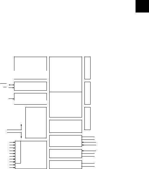
The MC68HC05B6 microcomputer (MCU) is a member of Motorola’s MC68HC05 family of low-cost single chip microcomputers. This 8-bit MCU contains an on-chip oscillator, CPU, RAM, ROM, EEPROM, A/D converter, pulse length modulated outputs, I/O, serial communications interface, programmable timer system and watchdog. The fully static design allows operation at frequencies down to dc to further reduce the already low power consumption to a few micro-amps.
This data sheet is structured such that devices similar to the MC68HC05B6 are described in a set of appendices (see Table 1-1).
Table 1-1 Data sheet appendices
Device |
Appendix |
Differences from MC68HC05B6 |
|
|
|
|
|
MC68HC05B4 |
A |
4K bytes ROM; no EEPROM |
|
|
|
|
|
MC68HC05B8 |
B |
7.25K bytes ROM |
|
|
|
|
|
MC68HC705B5 |
C |
6K bytes EPROM; self-check replaced by bootstrap |
|
firmware; no EEPROM |
|||
|
|
||
|
|
|
|
MC68HC05B16 |
D |
16K bytes ROM; increased RAM and self-check ROM |
|
|
|
|
|
MC68HC705B16 |
E |
16K bytes EPROM; increased RAM; self-check replaced |
|
by bootstrap firmware; modified power-on reset routine |
|||
|
|
||
|
|
|
|
MC68HC05B32 |
F |
32K bytes ROM; no page zero ROM; increased RAM |
|
|
|
|
|
MC68HC705B32 |
G |
32K bytes EPROM; no page zero ROM; increased RAM; |
|
self-check mode replaced by bootstrap firmware |
|||
|
|
||
|
|
|
MC68HC05B6 |
INTRODUCTION |
MOTOROLA |
|
|
1-1 |

1
1.1Features
Hardware features
•Fully static design featuring the industry standard M68HC05 family CPU core
•On chip crystal oscillator with divide by 2 or a software selectable divide by 32 option (SLOW mode)
•2.1 MHz internal operating frequency at 5V; 1.0 MHz at 3V
•176 bytes of RAM
•5936 bytes of user ROM plus 14 bytes of user vectors
•256 bytes of byte erasable EEPROM with internal charge pump and security bit
•Write/erase protect bit for 224 of the 256 bytes EEPROM
•Self test/bootstrap mode
•Power saving STOP, WAIT and SLOW modes
•Three 8-bit parallel I/O ports and one 8-bit input-only port
•Software option available to output the internal E-clock to port pin PC2
•16-bit timer with 2 input captures and 2 output compares
•Computer operating properly (COP) watchdog timer
•Serial communications interface system (SCI) with independent transmitter/receiver baud rate selection; receiver wake-up function for use in multi-receiver systems
•8 channel A/D converter
•2 pulse length modulation systems which can be used as D/A converters
•One interrupt request input plus 4 on-board hardware interrupt sources
•Available in 52-pin plastic leaded chip carrier (PLCC), 64-pin quad flat pack (QFP) and 56-pin shrink dual in line (SDIP) packages
•Complete development system support available using the MMDS05 development station with the M68HC05BEM emulation module or the M68HC05BEVS evaluation system
1.2Mask options for the MC68HC05B6
The MC68HC05B6 has three mask options that are programmed during manufacture and must be specified on the order form.
•Power-on-reset delay (tPORL) = 16 or 4064 cycles
MOTOROLA |
INTRODUCTION |
MC68HC05B6 |
1-2 |
|
|
1
•Automatic watchdog enable/disable following a power-on or external reset
•Watchdog enable/disable during WAIT mode
Warning: It is recommended that an external clock is always used if tPORL is set to 16 cycles. This will prevent any problems arising with oscillator stability when the device is put into
STOP mode.
VPP1 
RESET
IRQ
OSC2 
OSC1
VDD
VSS
PD0/AN0 |
|
|
PD1/AN1 |
|
|
PD2/AN2 |
D |
|
PD3/AN3 |
||
Port |
||
PD4/AN4 |
||
PD5/AN5 |
|
|
PD6/AN6 |
|
|
PD7/AN7 |
|
|
VRH |
|
|
VRL |
|
256 bytes EEPROM
Charge pump
COP watchdog
Oscillator
2 / 32
M68HC05
CPU
8-bit A/D converter
5950 bytes User ROM (including 14 bytes User vectors)
432 bytes self check ROM
176 bytes RAM
16-bit programmable timer
SCI
PLM
Port A
Port B
Port C

 PA0
PA0

 PA1
PA1

 PA2
PA2

 PA3
PA3

 PA4
PA4

 PA5
PA5

 PA6
PA6

 PA7
PA7

 PB0
PB0

 PB1
PB1

 PB2
PB2

 PB3
PB3

 PB4
PB4

 PB5
PB5

 PB6
PB6

 PB7
PB7

 PC0
PC0

 PC1
PC1

 PC2/ECLK

 PC3
PC3

 PC4
PC4

 PC5
PC5

 PC6
PC6 
 PC7
PC7
 TCMP1
TCMP1
 TCMP2
TCMP2
TCAP1
TCAP2
RDI
 SCLK
SCLK
 TDO
TDO
 PLMA D/A
 PLMB D/A
Figure 1-1 MC68HC05B6 block diagram
MC68HC05B6 |
INTRODUCTION |
MOTOROLA |
|
|
1-3 |

1
THIS PAGE INTENTIONALLY LEFT BLANK
MOTOROLA |
INTRODUCTION |
MC68HC05B6 |
1-4 |
|
|

2
2
MODES OF OPERATION AND PIN
DESCRIPTIONS
2.1Modes of operation
The MC68HC05B6 MCU has two modes of operation, namely single chip and self check modes. Table 2-1 shows the conditions required to enter each mode on the rising edge of RESET.
Table 2-1 Mode of operation selection
IRQ pin |
TCAP1 pin |
PD3 |
PD4 |
Mode |
VSS to VDD |
VSS to VDD |
X |
X |
Single chip |
2VDD |
VDD |
0 |
X |
Self-check |
2VDD |
VDD |
1 |
0 |
Serial RAM loader |
2VDD |
VDD |
1 |
1 |
Jump to any address |
2.1.1Single chip mode
This is the normal operating mode of the MC68HC05B6. In this mode the device functions as a self-contained microcomputer (MCU) with all on-board peripherals, including the three 8-bit I/O ports and the 8-bit input-only port, available to the user. All address and data activity occurs within the MCU.
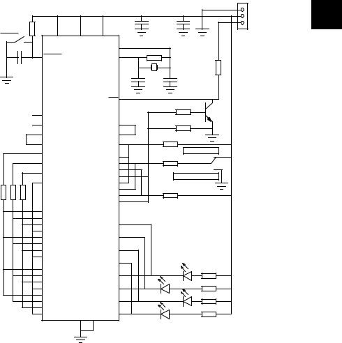
2.1.2Self-check mode
The self-check function available on the MC68HC05B6 provides an internal capability to determine if the device is functional. Self-check is performed using the circuit shown in Figure 2-1. Port C pins PC0–PC3 are monitored for the self-check results (light emitting diodes are shown but other devices could be used), and are interpreted as described in Table 2-2. The self-check mode
MC68HC05B6 |
MODES OF OPERATION AND PIN DESCRIPTIONS |
MOTOROLA |
|
|
2-1 |

is entered by applying 2 x VDD dc (via a 4.7k resistor) to theIRQ pin and 5V dc input (via a 4.7k 2 resistor) to the TCAP1 pin and then depressing the reset switch to execute a reset. After reset, the following tests are performed automatically and once completed they continually repeat. A good device will exhibit flashing LEDs; a bad device will be indicated by the LEDs holding at one value.
I/0 |
— |
|
Functionally exercises ports A, B, C and D |
||||
RAM |
— |
|
Counter test for each RAM byte |
||||
ROM |
— |
|
Exclusive OR with odd ones parity result |
||||
Timer |
— |
|
Tracks counter registers and checks ICF1, ICF2, OCF1, |
||||
|
|
|
|
OCF2 and TOF flags |
|||
SCI |
— |
|
Transmission test; check for RDRF, TDRE, TC and FE |
||||
|
|
|
|
flags |
|
|
|
A/D |
— |
|
Check A/D functionality on internal channels: VRL, VRH |
||||
|
|
|
|
and (VRL + VRH)/2 |
|||
EEPROM |
— |
|
This test is optional; it executes a write/erase test of the |
||||
|
|
|
|
256 bytes EEPROM (available only for the MC68HC05B6 |
|||
|
|
|
|
version), and then deactivates the security bit. |
|||
PLM |
— |
|
Checks the PLM basic functionality |
||||
Interrupts |
— |
|
Tests external timer and SCI interrupts |
||||
Watchdog |
— |
|
Tests the watchdog |
||||
|
|
Table 2-2 MC68HC05B6 self-check results |
|||||
|
|
|
|
|
|
|
|
|
|
PC3 |
PC2 |
PC1 |
PC0 |
Remarks |
|
|
|
|
|
|
|
|
|
|
|
1 |
0 |
0 |
1 |
Bad port |
|
|
|
|
|
|
|
|
|
|
|
0 |
1 |
1 |
0 |
Bad port |
|
|
|
|
|
|
|
|
|
|
|
1 |
0 |
1 |
0 |
Bad RAM |
|
|
|
|
|
|
|
|
|
|
|
1 |
0 |
1 |
1 |
Bad ROM |
|
|
|
|
|
|
|
|
|
|
|
1 |
1 |
0 |
0 |
Bad Timer |
|
|
|
|
|
|
|
|
|
|
|
1 |
1 |
0 |
1 |
Bad SCI |
|
|
|
|
|
|
|
|
|
|
|
1 |
1 |
1 |
0 |
Bad A/D |
|
|
|
|
|
|
|
|
|
|
|
0 |
0 |
0 |
0 |
Bad EEPROM (or other if B4) |
|
|
|
|
|
|
|
|
|
|
|
0 |
0 |
0 |
1 |
Bad PLM |
|
|
|
|
|
|
|
|
|
|
|
0 |
0 |
1 |
0 |
Bad interrupts |
|
|
|
|
|
|
|
|
|
|
|
0 |
0 |
1 |
1 |
Bad watchdog |
|
|
|
|
|
|
|
|
|
|
|
|
Flashing |
|
Good device |
|
|
|
|
|
|
|
|
|
|
|
|
|
All others |
|
Bad device, bad port etc. |
|
|
|
|
|
|
|
|
|
|
‘0’ indicates LED on; ‘1’ indicates LED off
MOTOROLA |
MODES OF OPERATION AND PIN DESCRIPTIONS |
MC68HC05B6 |
2-2 |
|
|
|
|
|
|
|
|
|
|
P1 |
2 |
|
|
|
|
|
|
|
|
GND |
|
|
|
|
|
|
|
|
|
+5V |
|
|
|
|
|
|
10 nF |
47 µF |
2xVDD |
||
RESET |
15 |
8 |
|
10 |
|
|
|
|
|
NC |
VRH |
VDD |
|
|
|
|
|
||
|
16 |
|
|
|
|
||||
|
|
|
|
OSC1 |
10 M |
|
|
|
|
18 |
RESET |
|
|
|
17 |
|
|
|
|
|
|
OSC2 |
|
|
|
|
|||
|
|
|
|
|
|
|
|||
0.01 µF |
|
|
|
|
|
|
|
4k7 |
|
|
|
|
|
|
22 pF |
4 MHz |
22 pF |
|
|
|
|
|
|
|
|
|
|
|
|
|
|
|
|
IRQ 19 |
|
|
|
|
|
6 |
NC |
|
|
|
|
|
|
BC239 |
|
40 |
VPP1 |
|
|
TCAP2 23 |
|
|
|
|
|
50 |
RDI |
package) |
|
TCMP2 |
1 |
|
4k7 |
|
|
52 |
|
|
TCAP1 22 |
|
|
|
|||
TDO |
|
|
|
|
|
||||
20 |
PLMA |
|
PB7 |
32 |
|
4k7 |
EEPROM tested |
|
|
21 |
PLMB |
-pin |
|
PB6 |
33 |
|
|
|
|
|
|
34 |
|
|
|
|
|||
2 |
TCMP1 |
|
PB5 |
|
|
|
|
||
|
(52 |
|
PB4 |
35 |
|
|
EEPROM not tested |
|
|
51 |
|
|
36 |
|
|
|
|||
SCLK |
|
PB3 |
|
|
|
|
|||
MC68HC05B6 |
|
|
|
|
|
||||
|
|
|
PB2 |
37 |
|
4k7 |
|
|
|
|
|
|
PB1 |
38 |
|
|
|
|
|
|
|
|
PB0 |
39 |
|
|
|
|
|
3 |
PD7 |
|
|
|
|
|
|
|
|
4 |
PD6 |
|
|
|
|
|
|
|
|
5 |
PD5 |
|
|
PC7 |
42 |
|
|
|
|
9 |
PD4 |
|
|
PC6 43 |
|
|
|
|
|
11 |
PD3 |
|
|
|
|
|
|
||
12 |
PD2 |
|
|
PC5 44 |
|
|
|
|
|
13 |
PD1 |
|
|
|
|
|
|
||
14 |
PD0 |
|
|
PC4 45 |
|
|
|
|
|
24 |
|
|
|
|
|
|
|
||
PA7 |
|
|
PC3 46 |
|
|
680 |
|
||
25 |
PA6 |
|
|
|
|
|
|
||
26 |
PA5 |
|
|
PC2 47 |
|
|
680 |
|
|
27 |
PA4 |
|
|
|
|
|
|
||
28 |
PA3 |
|
|
PC1 48 |
|
|
680 |
|
|
29 |
PA2 |
|
|
|
|
|
|
||
30 |
PA1 |
|
|
PC0 49 |
|
|
680 |
|
|
31 |
PA0 |
VSS VRL |
|
|
|
|
|||
|
|
41 |
7 |
|
|
|
|
|
|
Note: For the MC68HC05B4, switches on PB5 and PB6 have no effect
All resistors are 10 k , unless otherwise stated.
Figure 2-1 MC68HC05B6 self-check schematic diagram
MC68HC05B6 |
MODES OF OPERATION AND PIN DESCRIPTIONS |
MOTOROLA |
|
|
2-3 |

2.2Serial RAM loader
2
The ‘load program in RAM and execute’ mode is entered if the following conditions are satisfied when the reset pin is released to VDD. The format used is identical to the format used for the MC68HC805C4. The SEC bit in the options register must be inactive, i.e. set to ‘1’.
–IRQ at 2xVDD
–TCAP1 at VDD
–PD3 at VDD for at least 30 machine cycles after reset
–PD4 at VSS for at least 30 machine cycles after reset
In the ‘load program in RAM and execute’ routine, user programs are loaded into MCU RAM via the SCI port and then executed. Data is loaded sequentially, starting at RAM location $0050, until the last byte is loaded. Program control is then transferred to the RAM program starting at location $0051. The first byte loaded is the count of the total number of bytes in the program plus the count byte. The program starts at the second byte in RAM. During the firmware initialization stage, the SCI is configured for the NRZ data format (idle line, start bit, eight data bits and stop bit). The baud rate is 9600 with a 4 MHz crystal. A program to convert ASCII S-records to the format required by the RAM loader is available from Motorola.
If immediate execution is not desired after loading the RAM program, it is possible to hold off execution. This is accomplished by setting the byte count to a value that is greater than the overall length of the loaded data. When the last byte is loaded, the firmware will halt operation expecting additional data to arrive. At this point, the reset switch is placed in the reset position which will reset the MCU, but keep the RAM program intact. All routines can now be entered from this state, including the one which will execute the program in RAM (see Section 2.3).
To load a program in the EEPROM, the ‘load program in RAM and execute’ function is also used. In this instance the process involves two distinct steps. Firstly, the RAM is loaded with a program which will control the loading of the EEPROM, and when the RAM contents are executed, the MCU is instructed to load the EEPROM.
The erased state of the EEPROM is $FF.
Figure 2-2 shows the schematic diagram of the circuit required for the serial RAM loader.
2.3‘Jump to any address’
The ‘jump to any address’ mode is entered when the reset pin is released to VDD, if the following conditions are satisfied:
–IRQ at 2xVDD
–TCAP1 at VDD
–PD3 at VDD for at least 30 machine cycles after reset
–PD4 at VDD for at least 30 machine cycles after reset
MOTOROLA |
MODES OF OPERATION AND PIN DESCRIPTIONS |
MC68HC05B6 |
2-4 |
|
|
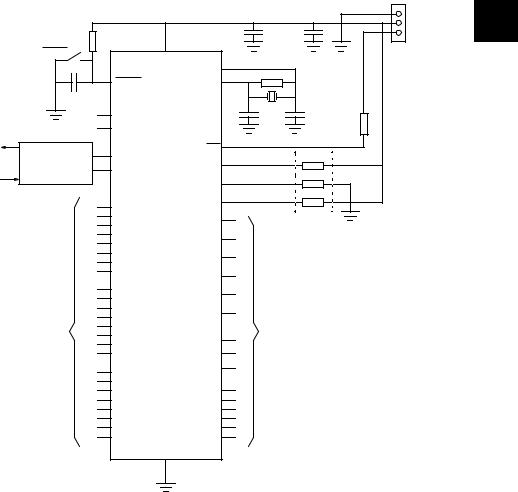
|
|
|
|
|
|
|
|
|
P1 |
2 |
|
|
|
|
|
|
|
|
|
GND |
|
|
|
|
|
|
|
|
|
|
+5V |
|
|
|
10 k |
|
|
|
10 nF |
47 µF |
2xVDD |
||
|
|
|
10 |
|
|
|
|
|
|
|
|
RESET |
|
|
|
|
|
|
|
|
|
|
|
|
VDD |
|
|
|
|
|
|
|
|
|
|
|
|
16 |
|
|
|
|
|
|
|
|
|
|
OSC1 |
10 M |
|
|
|
|
|
|
18 |
RESET |
|
|
17 |
|
|
|
|
|
|
|
OSC2 |
|
|
|
|
|||
|
0.01 µF |
|
|
|
|
|
|
|
|
|
|
|
6 |
|
|
|
22 pF |
4 MHz |
22 pF |
|
|
|
|
NC |
|
|
|
|
|
|
||
|
|
|
|
|
|
|
|
10 k |
|
|
|
|
15 |
NC |
|
|
|
|
|
|
|
|
|
|
|
|
|
|
|
|
|
|
9600 Bd |
|
|
|
|
|
19 |
|
|
|
|
|
RS232 level translator |
50 |
|
|
IRQ |
|
|
|
|
|
|
RDI |
|
|
|
|
10 k |
|
|
||
|
|
|
|
11 |
|
|
|
|||
RS232 |
suggested: |
52 |
TDO |
|
PD3 |
|
|
|
|
|
MC145406 or MAX232 |
|
|
|
|
|
10 k |
3 x 10 k |
|
||
|
|
|
|
9 |
|
|
||||
|
|
|
|
|
PD4 |
|
|
|
|
|
|
|
|
|
|
|
22 |
|
10 k |
|
|
|
|
24 |
PA7 |
package) |
TCAP1 |
|
|
|
|
|
|
|
27 |
|
|
|
|
|
|
||
|
|
25 |
PA6 |
|
VRH |
8 |
|
optional |
|
|
|
|
26 |
|
|
|
|
||||
|
|
|
PA5 |
|
|
|
|
|
|
|
|
|
28 |
PA4 |
-pin |
VRL |
7 |
|
|
|
|
|
|
29 |
PA3 |
|
|
|
|
|
|
|
|
|
PA2 |
(52 |
|
40 |
|
|
|
|
|
|
|
30 |
VPP1 |
|
|
|
|
|||
|
|
31 |
PA1 |
MC68HC05B6 |
|
|
|
|
|
|
|
|
PA0 |
|
20 |
|
|
|
|
||
|
|
|
|
PLMA |
|
|
|
|
||
|
|
32 |
PB7 |
|
|
21 |
|
|
|
|
|
|
33 |
|
PLMB |
|
|
|
|
||
|
|
34 |
PB6 |
|
|
|
|
|
|
|
|
|
PB5 |
|
|
51 |
|
|
|
|
|
|
|
35 |
|
SCLK |
|
|
|
|
||
Connect as required |
36 |
PB4 |
|
|
|
Connect as required |
|
|
||
PB3 |
|
|
|
|
|
|||||
for the application |
37 |
|
|
|
for the application |
|
|
|||
PB2 |
|
|
1 |
|
|
|||||
|
|
38 |
|
TCMP2 |
|
|
|
|
||
|
|
39 |
PB1 |
|
|
23 |
|
|
|
|
|
|
PB0 |
|
TCAP2 |
|
|
|
|
||
|
|
42 |
PC7 |
|
TCMP1 |
2 |
|
|
|
|
|
|
43 |
|
|
|
|
|
|
|
|
|
|
PC6 |
|
|
|
|
|
|
|
|
|
|
44 |
|
|
3 |
|
|
|
|
|
|
|
PC5 |
|
PD7 |
|
|
|
|
||
|
|
45 |
PC4 |
|
PD6 |
4 |
|
|
|
|
|
|
46 |
PC3 |
|
PD5 |
5 |
|
|
|
|
|
|
47 |
PC2 |
|
PD2 |
12 |
|
|
|
|
|
|
48 |
PC1 |
|
PD1 |
13 |
|
|
|
|
|
|
49 |
PC0 |
|
PD0 |
14 |
|
|
|
|
|
|
|
|
VSS |
|
|
|
|
|
|
|
|
|
|
41 |
|
|
|
|
|
|
Figure 2-2 MC68HC05B6 ‘load program in RAM and execute’ schematic diagram
This function allows execution of programs previously loaded in RAM or EEPROM using the methods outlined in Section 2.2.
To execute the ‘jump to any address’ function, data input at port A has to be $CC and data input at port B and port C should represent the MSB and LSB respectively, of the address to jump to for execution of the user program. A schematic diagram of the circuit required is shown in Figure 2-3.
MC68HC05B6 |
MODES OF OPERATION AND PIN DESCRIPTIONS |
MOTOROLA |
|
|
2-5 |

2 |
|
|
|
|
|
|
|
|
P1 |
|
|
|
|
|
|
|
|
GND |
|
|
|
|
|
|
10 nF |
47 µF |
+5V |
||
|
|
10 k |
|
|
|
2xVDD |
|||
|
|
|
10 |
|
|
|
|
|
|
|
RESET |
|
|
|
|
|
|
|
|
|
|
|
VDD |
|
|
|
|
|
|
|
|
|
|
|
16 |
|
|
|
|
|
|
|
|
|
OSC1 |
10 M |
|
|
|
|
|
18 |
RESET |
|
|
17 |
|
|
|
|
|
|
OSC2 |
|
|
|
|||
|
0.01 µF |
|
|
|
|
|
|
|
|
|
|
6 |
|
|
|
22 pF |
4 MHz |
22 pF |
|
|
|
NC |
|
|
|
|
|
||
|
|
|
|
|
|
|
|
10 k |
|
|
|
15 |
NC |
|
|
|
|
|
|
|
|
|
|
|
|
|
|
|
|
|
|
|
|
|
IRQ |
19 |
|
|
|
|
8 x 10 k optional (see note) |
|
|
|
11 |
|
10 k |
|
|
|
|
24 |
|
|
PD3 |
|
|
|
|
|
|
PA7 |
|
|
|
|
10 k |
3 x 10 k |
|
|
|
25 |
|
|
9 |
|
|||
|
|
PA6 |
|
PD4 |
|
|
|
||
|
|
26 |
PA5 |
|
|
22 |
|
10 k |
|
|
|
27 |
|
|
|
|
|||
|
|
PA4 |
package) |
TCAP1 |
|
|
|
||
|
|
28 |
PA1 |
|
|
|
|
|
|
|
|
29 |
PA3 |
|
|
8 |
|
optional |
|
|
|
PA2 |
|
VRH |
|
|
|||
|
|
30 |
|
|
|
|
|
|
|
|
|
31 |
PA0 |
(52-pin |
VRL |
7 |
|
|
|
|
MSB |
36 |
PB3 |
VPP1 |
40 |
|
|
|
|
|
MC68HC05B6 |
SCLK |
51 |
|
|
|
|||
|
8 x 10 k |
32 |
|
|
|
20 |
|
|
|
|
|
PB7 |
|
PLMA |
|
|
|
||
|
|
33 |
PB6 |
|
|
|
|
|
|
|
|
34 |
PB5 |
|
PLMB |
21 |
|
|
|
|
|
35 |
PB4 |
|
|
|
|
|
|
|
|
|
|
|
|
|
|
|
|
address |
|
37 |
PB0 |
|
TDO |
52 |
Connect as required |
|
|
|
39 |
|
|
||||||
|
|
38 |
PB2 |
|
RDI |
50 |
|
||
|
|
PB1 |
|
|
for the application |
|
|||
required |
|
|
|
|
|
|
|||
|
|
PC7 |
|
TCMP2 |
1 |
|
|
|
|
|
|
|
|
|
|
|
|
||
Select |
8 x 10 k |
42 |
|
|
TCAP2 |
23 |
|
|
|
LSB |
46 |
PC3 |
|
PD7 |
4 |
|
|
|
|
|
|
43 |
PC6 |
|
TCMP1 |
2 |
|
|
|
|
|
44 |
PC5 |
|
|
|
|
|
|
|
|
45 |
|
|
|
|
|
|
|
|
|
PC4 |
|
|
3 |
|
|
|
|
|
|
|
|
|
|
|
|
||
|
|
47 |
PC2 |
|
PD6 |
5 |
|
|
|
|
|
48 |
|
PD5 |
|
|
|
||
|
|
49 |
PC1 |
|
PD2 |
12 |
|
|
|
|
|
PC0 |
|
13 |
|
|
|
||
|
|
|
|
|
PD1 |
14 |
|
|
|
|
|
|
|
VSS |
PD0 |
|
|
|
|
|
|
|
|
41 |
|
|
|
|
|
Note: These eight resistors are optional; direct connection is possible if pins PA0-PA7, PB0-PB7 and PC0-PC7 are kept in input mode during application.
Figure 2-3 MC68HC05B6 ‘jump to any address’ schematic diagram
MOTOROLA |
MODES OF OPERATION AND PIN DESCRIPTIONS |
MC68HC05B6 |
2-6 |
|
|
 Loading...