


 Loading...
Motorola MC68HSC705C8ACS, MC68HSC705C8ACFS, MC68HSC705C8ACFB, MC68HSC705C8ACFN, MC68HSC705C8AC Datasheet
...MC68HC705C8A/D
Rev. 2.0
HC 5
5
MC68HC705C8A
MC68HSC705C8A
HCMOS Microcontroller Unit
TECHNICAL DATA

Technical Data
Motorola reserves the right to make changes without further notice to any products herein to improve reliability, function or design. Motorola does not assume any liability arising out of the application or use of any product or circuit described herein; neither does it convey any license under its patent rights nor the rights of others. Motorola products are not designed, intended, or authorized for use as components in systems intended for surgical implant into the body, or other applications intended to support or sustain life, or for any other application in which the failure of the Motorola product could create a situation where personal injury or death may occur. Should Buyer purchase or use Motorola products for any such unintended or unauthorized application, Buyer shall indemnify and hold Motorola and its officers, employees, subsidiaries, affiliates, and distributors harmless against all claims, costs, damages, and expenses, and reasonable attorney fees arising out of, directly or indirectly, any claim of personal injury or death associated with such unintended or unauthorized use, even if such claim alleges that Motorola was negligent regarding the design or manufacture of the part.
© Motorola, Inc., 1999 |
|
Technical Data |
MC68HC705C8A — Rev. 2.0 |
|
|
|
|
2 |
MOTOROLA |

Technical Data — MC68HC705C8A
List of Sections
Section 1. General Description . . . . . . . . . . . . . . . . . . . . 19
Section 2. Memory . . . . . . . . . . . . . . . . . . . . . . . . . . . . . . 33
Section 3. Central Processor Unit (CPU) . . . . . . . . . . . . 41
Section 4. Interrupts . . . . . . . . . . . . . . . . . . . . . . . . . . . . . 47
Section 5. Resets . . . . . . . . . . . . . . . . . . . . . . . . . . . . . . . 59
Section 6. Low-Power Modes. . . . . . . . . . . . . . . . . . . . . . 67
Section 7. Parallel Input/Output (I/O). . . . . . . . . . . . . . . . 75
Section 8. Capture/Compare Timer . . . . . . . . . . . . . . . . . 87
Section 9. EPROM/OTPROM (PROM) . . . . . . . . . . . . . . 101
Section 10. Serial Communications Interface (SCI) . . . 119
Section 11. Serial Peripheral Interface (SPI). . . . . . . . . 137
Section 12. Instruction Set . . . . . . . . . . . . . . . . . . . . . . . 151
Section 13. Electrical Specifications . . . . . . . . . . . . . . 169
Section 14. Mechanical Specifications . . . . . . . . . . . . . 189
Section 15. Ordering Information . . . . . . . . . . . . . . . . . 197
Appendix A. MC68HSC705C8A . . . . . . . . . . . . . . . . . . . 199
MC68HC705C8A — Rev. 2.0 |
|
Technical Data |
|
|
|
MOTOROLA |
List of Sections |
3 |

List of Sections
Technical Data |
|
MC68HC705C8A — Rev. 2.0 |
|
|
|
4 |
List of Sections |
MOTOROLA |

Technical Data — MC68HC705C8A
Table of Contents
Section 1. General Description
1.1 Contents . . . . . . . . . . . . . . . . . . . . . . . . . . . . . . . . . . . . . . . . . .19
1.2 Introduction . . . . . . . . . . . . . . . . . . . . . . . . . . . . . . . . . . . . . . . .20
1.3 Features . . . . . . . . . . . . . . . . . . . . . . . . . . . . . . . . . . . . . . . . . .20
1.4 Programmable Options. . . . . . . . . . . . . . . . . . . . . . . . . . . . . . .21
1.5 Block Diagram . . . . . . . . . . . . . . . . . . . . . . . . . . . . . . . . . . . . .22
1.6 Pin Assignments . . . . . . . . . . . . . . . . . . . . . . . . . . . . . . . . . . . .24
1.7 Pin Functions . . . . . . . . . . . . . . . . . . . . . . . . . . . . . . . . . . . . . .27
1.7.1 VDD and VSS. . . . . . . . . . . . . . . . . . . . . . . . . . . . . . . . . . . . .27
1.7.2 OSC1 and OSC2 . . . . . . . . . . . . . . . . . . . . . . . . . . . . . . . . .27
1.7.3 External Reset Pin (RESET) . . . . . . . . . . . . . . . . . . . . . . . .30
1.7.4 External Interrupt Request Pin (IRQ) . . . . . . . . . . . . . . . . . .30 1.7.5 Input Capture Pin (TCAP) . . . . . . . . . . . . . . . . . . . . . . . . . .30 1.7.6 Output Compare Pin (TCMP) . . . . . . . . . . . . . . . . . . . . . . . .30 1.7.7 Port A I/O Pins (PA7–PA0). . . . . . . . . . . . . . . . . . . . . . . . . .30 1.7.8 Port B I/O Pins (PB7–PB0). . . . . . . . . . . . . . . . . . . . . . . . . .30
1.7.9 Port C I/O Pins (PC7–PC0) . . . . . . . . . . . . . . . . . . . . . . . . .31 1.7.10 Port D I/O Pins (PD7 and PD5–PD0) . . . . . . . . . . . . . . . . . .31
Section 2. Memory
2.1 Contents . . . . . . . . . . . . . . . . . . . . . . . . . . . . . . . . . . . . . . . . . .33
2.2 Introduction . . . . . . . . . . . . . . . . . . . . . . . . . . . . . . . . . . . . . . . .33
2.3 Memory Map. . . . . . . . . . . . . . . . . . . . . . . . . . . . . . . . . . . . . . .33
2.4 Input/Output (I/O) . . . . . . . . . . . . . . . . . . . . . . . . . . . . . . . . . . .34
MC68HC705C8A — Rev. 2.0 |
|
Technical Data |
|
|
|
MOTOROLA |
Table of Contents |
5 |

Table of Contents
2.5 RAM . . . . . . . . . . . . . . . . . . . . . . . . . . . . . . . . . . . . . . . . . . . . .34
2.6 EPROM/OTPROM (PROM) . . . . . . . . . . . . . . . . . . . . . . . . . . .35
2.7 Bootloader ROM . . . . . . . . . . . . . . . . . . . . . . . . . . . . . . . . . . . .35
Section 3. Central Processor Unit (CPU)
3.1 Contents . . . . . . . . . . . . . . . . . . . . . . . . . . . . . . . . . . . . . . . . . .41
3.2 Introduction . . . . . . . . . . . . . . . . . . . . . . . . . . . . . . . . . . . . . . . .41
3.3 CPU Registers . . . . . . . . . . . . . . . . . . . . . . . . . . . . . . . . . . . . .42
3.3.1 Accumulator . . . . . . . . . . . . . . . . . . . . . . . . . . . . . . . . . . . .43
3.3.2 Index Register . . . . . . . . . . . . . . . . . . . . . . . . . . . . . . . . . . .43
3.3.3 Stack Pointer . . . . . . . . . . . . . . . . . . . . . . . . . . . . . . . . . . . .44
3.3.4 Program Counter . . . . . . . . . . . . . . . . . . . . . . . . . . . . . . . . .44
3.3.5 Condition Code Register . . . . . . . . . . . . . . . . . . . . . . . . . . .45
3.4 Arithmetic/Logic Unit (ALU) . . . . . . . . . . . . . . . . . . . . . . . . . . .46
Section 4. Interrupts
4.1 Contents . . . . . . . . . . . . . . . . . . . . . . . . . . . . . . . . . . . . . . . . . .47
4.2 Introduction . . . . . . . . . . . . . . . . . . . . . . . . . . . . . . . . . . . . . . . .47
4.3 Interrupt Sources . . . . . . . . . . . . . . . . . . . . . . . . . . . . . . . . . . .48
4.3.1 Software Interrupt. . . . . . . . . . . . . . . . . . . . . . . . . . . . . . . . .48
4.3.2 External Interrupt (IRQ) . . . . . . . . . . . . . . . . . . . . . . . . . . . .49
4.3.3 Port B Interrupts . . . . . . . . . . . . . . . . . . . . . . . . . . . . . . . . . .51
4.3.4 Capture/Compare Timer Interrupts . . . . . . . . . . . . . . . . . . .53
4.3.5 SCI Interrupts . . . . . . . . . . . . . . . . . . . . . . . . . . . . . . . . . . . .53
4.3.6 SPI Interrupts . . . . . . . . . . . . . . . . . . . . . . . . . . . . . . . . . . . .54
4.4 Interrupt Processing . . . . . . . . . . . . . . . . . . . . . . . . . . . . . . . . .55
Section 5. Resets
5.1 Contents . . . . . . . . . . . . . . . . . . . . . . . . . . . . . . . . . . . . . . . . . .59
5.2 Introduction . . . . . . . . . . . . . . . . . . . . . . . . . . . . . . . . . . . . . . . .59
Technical Data |
|
MC68HC705C8A — Rev. 2.0 |
|
|
|
6 |
Table of Contents |
MOTOROLA |
Table of Contents
5.3 Reset Sources . . . . . . . . . . . . . . . . . . . . . . . . . . . . . . . . . . . . .59
5.3.1 Power-On Reset (POR) . . . . . . . . . . . . . . . . . . . . . . . . . . . .60
5.3.2 External Reset . . . . . . . . . . . . . . . . . . . . . . . . . . . . . . . . . . .60
5.3.3Programmable and Non-Programmable
COP Watchdog Resets . . . . . . . . . . . . . . . . . . . . . . . . . .60
5.3.4 Clock Monitor Reset . . . . . . . . . . . . . . . . . . . . . . . . . . . . . . .65
Section 6. Low-Power Modes
6.1 Contents . . . . . . . . . . . . . . . . . . . . . . . . . . . . . . . . . . . . . . . . . .67
6.2 Introduction . . . . . . . . . . . . . . . . . . . . . . . . . . . . . . . . . . . . . . . .67
6.3 Stop Mode . . . . . . . . . . . . . . . . . . . . . . . . . . . . . . . . . . . . . . . .67
6.3.1 SCI During Stop Mode . . . . . . . . . . . . . . . . . . . . . . . . . . . . .69 6.3.2 SPI During Stop Mode . . . . . . . . . . . . . . . . . . . . . . . . . . . . .69 6.3.3 Programmable COP Watchdog in Stop Mode . . . . . . . . . . .69 6.3.4 Non-Programmable COP Watchdog in Stop Mode . . . . . . .71
6.4 Wait Mode. . . . . . . . . . . . . . . . . . . . . . . . . . . . . . . . . . . . . . . . .71
6.4.1 Programmable COP Watchdog in Wait Mode . . . . . . . . . . .73 6.4.2 Non-Programmable COP Watchdog in Wait Mode . . . . . . .73
6.5 Data-Retention Mode . . . . . . . . . . . . . . . . . . . . . . . . . . . . . . . .73
Section 7. Parallel Input/Output (I/O)
7.1 Contents . . . . . . . . . . . . . . . . . . . . . . . . . . . . . . . . . . . . . . . . . .75
7.2 Introduction . . . . . . . . . . . . . . . . . . . . . . . . . . . . . . . . . . . . . . . .75
7.3 Port A . . . . . . . . . . . . . . . . . . . . . . . . . . . . . . . . . . . . . . . . . . . .76
7.3.1 Port A Data Register . . . . . . . . . . . . . . . . . . . . . . . . . . . . . .76
7.3.2 Data Direction Register A. . . . . . . . . . . . . . . . . . . . . . . . . . .77
7.3.3 Port A Logic . . . . . . . . . . . . . . . . . . . . . . . . . . . . . . . . . . . . .78
7.4 Port B . . . . . . . . . . . . . . . . . . . . . . . . . . . . . . . . . . . . . . . . . . . .79
7.4.1 Port B Data Register . . . . . . . . . . . . . . . . . . . . . . . . . . . . . .79
7.4.2 Data Direction Register B. . . . . . . . . . . . . . . . . . . . . . . . . . .80
7.4.3 Port B Logic . . . . . . . . . . . . . . . . . . . . . . . . . . . . . . . . . . . . .81
MC68HC705C8A — Rev. 2.0 |
|
Technical Data |
|
|
|
MOTOROLA |
Table of Contents |
7 |

Table of Contents
7.5 Port C . . . . . . . . . . . . . . . . . . . . . . . . . . . . . . . . . . . . . . . . . . . .83
7.5.1 Port C Data Register . . . . . . . . . . . . . . . . . . . . . . . . . . . . . .83
7.5.2 Data Direction Register C. . . . . . . . . . . . . . . . . . . . . . . . . . .84
7.5.3 Port C Logic . . . . . . . . . . . . . . . . . . . . . . . . . . . . . . . . . . . . .85
7.6 Port D . . . . . . . . . . . . . . . . . . . . . . . . . . . . . . . . . . . . . . . . . . . .86
Section 8. Capture/Compare Timer
8.1 Contents . . . . . . . . . . . . . . . . . . . . . . . . . . . . . . . . . . . . . . . . . .87
8.2 Introduction . . . . . . . . . . . . . . . . . . . . . . . . . . . . . . . . . . . . . . . .87
8.3 Timer Operation . . . . . . . . . . . . . . . . . . . . . . . . . . . . . . . . . . . .87
8.3.1 Input Capture . . . . . . . . . . . . . . . . . . . . . . . . . . . . . . . . . . . .90
8.3.2 Output Compare. . . . . . . . . . . . . . . . . . . . . . . . . . . . . . . . . .91
8.4 Timer I/O Registers. . . . . . . . . . . . . . . . . . . . . . . . . . . . . . . . . .92
8.4.1 Timer Control Register . . . . . . . . . . . . . . . . . . . . . . . . . . . . .92
8.4.2 Timer Status Register . . . . . . . . . . . . . . . . . . . . . . . . . . . . .94
8.4.3 Timer Registers . . . . . . . . . . . . . . . . . . . . . . . . . . . . . . . . . .95
8.4.4 Alternate Timer Registers. . . . . . . . . . . . . . . . . . . . . . . . . . .96
8.4.5 Input Capture Registers . . . . . . . . . . . . . . . . . . . . . . . . . . .98
8.4.6 Output Compare Registers. . . . . . . . . . . . . . . . . . . . . . . . . .99
Section 9. EPROM/OTPROM (PROM)
9.1 Contents . . . . . . . . . . . . . . . . . . . . . . . . . . . . . . . . . . . . . . . . .101
9.2 Introduction . . . . . . . . . . . . . . . . . . . . . . . . . . . . . . . . . . . . . . .101
9.3 EPROM/OTPROM (PROM) Programming . . . . . . . . . . . . . . .102
9.3.1 Program Register . . . . . . . . . . . . . . . . . . . . . . . . . . . . . . . .107
9.3.2 Preprogramming Steps . . . . . . . . . . . . . . . . . . . . . . . . . . .108
9.4 PROM Programming Routines . . . . . . . . . . . . . . . . . . . . . . . .109
9.4.1 Program and Verify PROM. . . . . . . . . . . . . . . . . . . . . . . . .109
9.4.2 Verify PROM Contents . . . . . . . . . . . . . . . . . . . . . . . . . . . .110 9.4.3 Secure PROM . . . . . . . . . . . . . . . . . . . . . . . . . . . . . . . . . .110 9.4.4 Secure PROM and Verify . . . . . . . . . . . . . . . . . . . . . . . . . .111 9.4.5 Secure PROM and Dump. . . . . . . . . . . . . . . . . . . . . . . . . .111 9.4.6 Load Program into RAM and Execute . . . . . . . . . . . . . . . .112
Technical Data |
|
MC68HC705C8A — Rev. 2.0 |
|
|
|
8 |
Table of Contents |
MOTOROLA |

Table of Contents
9.4.7 |
Execute Program in RAM. . . . . . . . . . . . . . . . . . . . . . . . . . |
113 |
9.4.8 |
Dump PROM Contents. . . . . . . . . . . . . . . . . . . . . . . . . . . . |
113 |
9.5 |
Control Registers . . . . . . . . . . . . . . . . . . . . . . . . . . . . . . . . . . |
114 |
9.5.1 |
Option Register . . . . . . . . . . . . . . . . . . . . . . . . . . . . . . . . . |
114 |
9.5.2 |
Mask Option Register 1 . . . . . . . . . . . . . . . . . . . . . . . . . . . |
115 |
9.5.3 |
Mask Option Register 2 . . . . . . . . . . . . . . . . . . . . . . . . . . . |
116 |
9.6 |
EPROM Erasing . . . . . . . . . . . . . . . . . . . . . . . . . . . . . . . . . . . |
117 |
Section 10. Serial Communications Interface (SCI) |
|
|
10.1 |
Contents . . . . . . . . . . . . . . . . . . . . . . . . . . . . . . . . . . . . . . . . . |
119 |
10.2 |
Introduction . . . . . . . . . . . . . . . . . . . . . . . . . . . . . . . . . . . . . . . |
119 |
10.3 |
Features . . . . . . . . . . . . . . . . . . . . . . . . . . . . . . . . . . . . . . . . . |
120 |
10.4 |
SCI Data Format. . . . . . . . . . . . . . . . . . . . . . . . . . . . . . . . . . . |
120 |
10.5 |
SCI Operation . . . . . . . . . . . . . . . . . . . . . . . . . . . . . . . . . . . . . |
121 |
10.5.1 |
Transmitter . . . . . . . . . . . . . . . . . . . . . . . . . . . . . . . . . . . . . |
121 |
10.5.2 |
Receiver . . . . . . . . . . . . . . . . . . . . . . . . . . . . . . . . . . . . . . . |
125 |
10.6 |
SCI I/O Registers . . . . . . . . . . . . . . . . . . . . . . . . . . . . . . . . . . |
127 |
10.6.1 |
SCI Data Register . . . . . . . . . . . . . . . . . . . . . . . . . . . . . . . |
127 |
10.6.2 |
SCI Control Register 1 . . . . . . . . . . . . . . . . . . . . . . . . . . . . |
128 |
10.6.3 |
SCI Control Register 2 . . . . . . . . . . . . . . . . . . . . . . . . . . . . |
129 |
10.6.4 |
SCI Status Register . . . . . . . . . . . . . . . . . . . . . . . . . . . . . . |
131 |
10.6.5 |
Baud Rate Register . . . . . . . . . . . . . . . . . . . . . . . . . . . . . . |
134 |
|
Section 11. Serial Peripheral Interface (SPI) |
|
11.1 |
Contents . . . . . . . . . . . . . . . . . . . . . . . . . . . . . . . . . . . . . . . . . |
137 |
11.2 |
Introduction . . . . . . . . . . . . . . . . . . . . . . . . . . . . . . . . . . . . . . . |
137 |
11.3 |
Features . . . . . . . . . . . . . . . . . . . . . . . . . . . . . . . . . . . . . . . . . |
138 |
11.4 |
Operation . . . . . . . . . . . . . . . . . . . . . . . . . . . . . . . . . . . . . . . . |
140 |
11.4.1 |
Pin Functions in Master Mode . . . . . . . . . . . . . . . . . . . . . . |
141 |
11.4.2 |
Pin Functions in Slave Mode . . . . . . . . . . . . . . . . . . . . . . . |
142 |
11.5 |
Multiple-SPI Systems . . . . . . . . . . . . . . . . . . . . . . . . . . . . . . . |
143 |
MC68HC705C8A — Rev. 2.0 |
Technical Data |
|
MOTOROLA |
Table of Contents |
9 |

Table of Contents
11.6 Serial Clock Polarity and Phase . . . . . . . . . . . . . . . . . . . . . . .144
11.7 SPI Error Conditions . . . . . . . . . . . . . . . . . . . . . . . . . . . . . . . .145
11.7.1 Mode Fault Error . . . . . . . . . . . . . . . . . . . . . . . . . . . . . . . .145
11.7.2 Write Collision Error . . . . . . . . . . . . . . . . . . . . . . . . . . . . . .145
11.7.3 Overrun Error . . . . . . . . . . . . . . . . . . . . . . . . . . . . . . . . . . .146
11.8 SPI Interrupts . . . . . . . . . . . . . . . . . . . . . . . . . . . . . . . . . . . . .146
11.9 SPI I/O Registers . . . . . . . . . . . . . . . . . . . . . . . . . . . . . . . . . .146
11.9.1 SPI Data Register. . . . . . . . . . . . . . . . . . . . . . . . . . . . . . . .147
11.9.2 SPI Control Register. . . . . . . . . . . . . . . . . . . . . . . . . . . . . .147
11.9.3 SPI Status Register . . . . . . . . . . . . . . . . . . . . . . . . . . . . . .149
Section 12. Instruction Set
12.1 Contents . . . . . . . . . . . . . . . . . . . . . . . . . . . . . . . . . . . . . . . . .151
12.2 Introduction . . . . . . . . . . . . . . . . . . . . . . . . . . . . . . . . . . . . . . .152
12.3 Addressing Modes . . . . . . . . . . . . . . . . . . . . . . . . . . . . . . . . .152
12.3.1 Inherent . . . . . . . . . . . . . . . . . . . . . . . . . . . . . . . . . . . . . . .153
12.3.2 Immediate. . . . . . . . . . . . . . . . . . . . . . . . . . . . . . . . . . . . . .153
12.3.3 Direct . . . . . . . . . . . . . . . . . . . . . . . . . . . . . . . . . . . . . . . . .153
12.3.4 Extended . . . . . . . . . . . . . . . . . . . . . . . . . . . . . . . . . . . . . .153
12.3.5 Indexed, No Offset . . . . . . . . . . . . . . . . . . . . . . . . . . . . . . .154
12.3.6 Indexed, 8-Bit Offset. . . . . . . . . . . . . . . . . . . . . . . . . . . . . .154
12.3.7 Indexed, 16-Bit Offset. . . . . . . . . . . . . . . . . . . . . . . . . . . . .154
12.3.8 Relative . . . . . . . . . . . . . . . . . . . . . . . . . . . . . . . . . . . . . . .155
12.4 Instruction Types . . . . . . . . . . . . . . . . . . . . . . . . . . . . . . . . . .155
12.4.1 Register/Memory Instructions. . . . . . . . . . . . . . . . . . . . . . .156
12.4.2 Read-Modify-Write Instructions . . . . . . . . . . . . . . . . . . . . .157
12.4.3 Jump/Branch Instructions. . . . . . . . . . . . . . . . . . . . . . . . . .158
12.4.4 Bit Manipulation Instructions . . . . . . . . . . . . . . . . . . . . . . .160
12.4.5 Control Instructions . . . . . . . . . . . . . . . . . . . . . . . . . . . . . .161
12.5 Instruction Set Summary . . . . . . . . . . . . . . . . . . . . . . . . . . . .162
12.6 Opcode Map . . . . . . . . . . . . . . . . . . . . . . . . . . . . . . . . . . . . . .167
Technical Data |
|
MC68HC705C8A — Rev. 2.0 |
|
|
|
10 |
Table of Contents |
MOTOROLA |
Table of Contents
Section 13. Electrical Specifications
13.1 Contents . . . . . . . . . . . . . . . . . . . . . . . . . . . . . . . . . . . . . . . . .169
13.2 Introduction . . . . . . . . . . . . . . . . . . . . . . . . . . . . . . . . . . . . . . .169
13.3 Maximum Ratings . . . . . . . . . . . . . . . . . . . . . . . . . . . . . . . . . .170
13.4 Operating Temperature Range. . . . . . . . . . . . . . . . . . . . . . . .171
13.5 Thermal Characteristics . . . . . . . . . . . . . . . . . . . . . . . . . . . . .171
13.6 Power Considerations. . . . . . . . . . . . . . . . . . . . . . . . . . . . . . .172
13.7 5.0-Volt DC Electrical Characteristics. . . . . . . . . . . . . . . . . . .173
13.8 3.3-Volt DC Electrical Characteristics . . . . . . . . . . . . . . . . . .174
13.9 5.0-Volt Control Timing . . . . . . . . . . . . . . . . . . . . . . . . . . . . . .179
13.10 3.3-Volt Control Timing . . . . . . . . . . . . . . . . . . . . . . . . . . . . . .180
13.11 5.0-Volt Serial Peripheral Interface (SPI) Timing . . . . . . . . . .183
13.12 3.3-Volt Serial Peripheral Interface (SPI) Timing . . . . . . . . . .185
Section 14. Mechanical Specifications
14.1 Contents . . . . . . . . . . . . . . . . . . . . . . . . . . . . . . . . . . . . . . . . .189
14.2 Introduction . . . . . . . . . . . . . . . . . . . . . . . . . . . . . . . . . . . . . . .189
14.3 40-Pin Plastic Dual In-Line Package (PDIP). . . . . . . . . . . . . .190
14.4 40-Pin Ceramic Dual In-Line Package (Cerdip) . . . . . . . . . . .191
14.5 44-Lead Plastic-Leaded Chip Carrier (PLCC) . . . . . . . . . . . .192 14.6 44-Lead Ceramic-Leaded Chip Carrier (CLCC) . . . . . . . . . . .193 14.7 44-Pin Quad Flat Pack (QFP). . . . . . . . . . . . . . . . . . . . . . . . .194 14.8 42-Pin Shrink Dual In-Line Package (SDIP) . . . . . . . . . . . . . .195
MC68HC705C8A — Rev. 2.0 |
|
Technical Data |
|
|
|
MOTOROLA |
Table of Contents |
11 |

Table of Contents
Section 15. Ordering Information
15.1 Contents . . . . . . . . . . . . . . . . . . . . . . . . . . . . . . . . . . . . . . . . .197
15.2 Introduction . . . . . . . . . . . . . . . . . . . . . . . . . . . . . . . . . . . . . . .197
15.3 MCU Order Numbers . . . . . . . . . . . . . . . . . . . . . . . . . . . . . . .197
Appendix A. MC68HSC705C8A
A.1 Contents . . . . . . . . . . . . . . . . . . . . . . . . . . . . . . . . . . . . . . . . .199
A.2 Introduction . . . . . . . . . . . . . . . . . . . . . . . . . . . . . . . . . . . . . . .199
A.3 5.0-Volt High-Speed DC Electrical Characteristics. . . . . . . . .200
A.4 3.3-Volt High-Speed DC Electrical Characteristics . . . . . . . .201
A.5 5.0-Volt High-Speed Control Timing . . . . . . . . . . . . . . . . . . . .202
A.6 3.3-Volt High-Speed Control Timing . . . . . . . . . . . . . . . . . . . .202
A.7 5.0-Volt High-Speed SPI Timing. . . . . . . . . . . . . . . . . . . . . . .203
A.8 3.3-Volt High-Speed SPI Timing. . . . . . . . . . . . . . . . . . . . . . .205
A.9 Ordering Information. . . . . . . . . . . . . . . . . . . . . . . . . . . . . . . .207
Index
Index . . . . . . . . . . . . . . . . . . . . . . . . . . . . . . . . . . . . . . . . . . . .209
Technical Data |
|
MC68HC705C8A — Rev. 2.0 |
|
|
|
12 |
Table of Contents |
MOTOROLA |

Technical Data — MC68HC705C8A
List of Figures
Figure |
Title |
Page |
1-1 Option Register (Option) . . . . . . . . . . . . . . . . . . . . . . . . . . .21
1-2 MC68HC705C8A Block Diagram . . . . . . . . . . . . . . . . . . . . .23
1-3 40-Pin PDIP/Cerdip Pin Assignments . . . . . . . . . . . . . . . . .24
1-4 44-Lead PLCC/CLCC Pin Assignments . . . . . . . . . . . . . . . .25
1-5 44-Pin QFP Pin Assignments. . . . . . . . . . . . . . . . . . . . . . . .25
1-6 42-Pin SDIP Pin Assignments . . . . . . . . . . . . . . . . . . . . . . .26
1-7 Bypassing Layout Recommendation . . . . . . . . . . . . . . . . . .27
1-8 Crystal Connections . . . . . . . . . . . . . . . . . . . . . . . . . . . . . . .28
1-9 2-Pin Ceramic Resonator Connections . . . . . . . . . . . . . . . .28
1-10 3-Pin Ceramic Resonator Connections . . . . . . . . . . . . . . . .29
1-11 External Clock . . . . . . . . . . . . . . . . . . . . . . . . . . . . . . . . . . .29
2-1 Memory Map . . . . . . . . . . . . . . . . . . . . . . . . . . . . . . . . . . . .36
2-2 I/O Register Summary . . . . . . . . . . . . . . . . . . . . . . . . . . . . .37
3-1 Programming Model . . . . . . . . . . . . . . . . . . . . . . . . . . . . . . .42
3-2 Accumulator (A) . . . . . . . . . . . . . . . . . . . . . . . . . . . . . . . . . .43
3-3 Index Register (X) . . . . . . . . . . . . . . . . . . . . . . . . . . . . . . . .43
3-4 Stack Pointer (SP) . . . . . . . . . . . . . . . . . . . . . . . . . . . . . . . .44
3-5 Program Counter (PC) . . . . . . . . . . . . . . . . . . . . . . . . . . . . .44
3-6 Condition Code Register (CCR) . . . . . . . . . . . . . . . . . . . . . .45
4-1 External Interrupt Internal Function Diagram . . . . . . . . . . . .50
4-2 External Interrupt Timing . . . . . . . . . . . . . . . . . . . . . . . . . . .50
4-3 Port B I/O Logic . . . . . . . . . . . . . . . . . . . . . . . . . . . . . . . . . .52
4-4 Interrupt Stacking Order . . . . . . . . . . . . . . . . . . . . . . . . . . . .56
4-5 Reset and Interrupt Processing Flowchart . . . . . . . . . . . . . .57
MC68HC705C8A — Rev. 2.0 |
|
Technical Data |
|
|
|
MOTOROLA |
List of Figures |
13 |

List of Figures
Figure |
Title |
Page |
5-1 |
Programmable COP Watchdog Diagram . . . . . . . . . . . . |
. . .61 |
5-2 |
Programmable COP Reset Register (COPRST) . . . . . . . |
. .62 |
5-3 |
Programmable COP Control Register (COPCR) . . . . . . . |
. .62 |
5-4 |
Non-Programmable COP Watchdog Diagram . . . . . . . . . |
. .65 |
6-1 |
Stop/Wait Mode Function Flowchart . . . . . . . . . . . . . . . . |
. .68 |
6-2 |
Programmable COP Watchdog |
|
|
in Stop Mode (PCOPE = 1) Flowchart. . . . . . . . . . . . . |
. .70 |
6-3 |
Non-Programmable COP Watchdog |
|
|
in Stop Mode (NCOPE = 1) Flowchart . . . . . . . . . . . . |
. .72 |
7-1 |
Port A Data Register (PORTA). . . . . . . . . . . . . . . . . . . . . |
. .76 |
7-2 |
Data Direction Register A (DDRA) . . . . . . . . . . . . . . . . . . |
. .77 |
7-3 |
Port A I/O Logic . . . . . . . . . . . . . . . . . . . . . . . . . . . . . . . . |
. .78 |
7-4 |
Port B Data Register (PORTB). . . . . . . . . . . . . . . . . . . . . |
. .79 |
7-5 |
Data Direction Register B (DDRB) . . . . . . . . . . . . . . . . . . |
. .80 |
7-6 |
Port B I/O Logic . . . . . . . . . . . . . . . . . . . . . . . . . . . . . . . . |
. .81 |
7-7 |
Port C Data Register (PORTC) . . . . . . . . . . . . . . . . . . . . |
. .83 |
7-8 |
Data Direction Register C (DDRC). . . . . . . . . . . . . . . . . . |
. .84 |
7-9 |
Port C I/O Logic . . . . . . . . . . . . . . . . . . . . . . . . . . . . . . . . |
. .85 |
7-10 |
Port D Fixed Input Register (PORTD) . . . . . . . . . . . . . . . |
. .86 |
8-1 |
Timer Block Diagram . . . . . . . . . . . . . . . . . . . . . . . . . . . . |
. .88 |
8-2 |
Timer I/O Register Summary . . . . . . . . . . . . . . . . . . . . . . |
. .89 |
8-3 |
Input Capture Operation. . . . . . . . . . . . . . . . . . . . . . . . . . |
. .90 |
8-4 |
Output Compare Operation . . . . . . . . . . . . . . . . . . . . . . . |
. .91 |
8-5 |
Timer Control Register (TCR) . . . . . . . . . . . . . . . . . . . . . |
. .92 |
8-6 |
Timer Status Register (TSR) . . . . . . . . . . . . . . . . . . . . . . |
. .94 |
8-7 |
Timer Registers (TRH and TRL) . . . . . . . . . . . . . . . . . . . |
. .95 |
8-8 |
Timer Register Reads . . . . . . . . . . . . . . . . . . . . . . . . . . . |
. .96 |
8-10 |
Alternate Timer Register Reads . . . . . . . . . . . . . . . . . . . . |
. .97 |
8-9 |
Alternate Timer Registers (ATRH and ATRL) . . . . . . . . . |
. .97 |
8-11 |
Input Capture Registers (ICRH and ICRL) . . . . . . . . . . . . |
. .98 |
8-12 |
Output Compare Registers (OCRH and OCRL). . . . . . . . |
. .99 |
Technical Data |
|
MC68HC705C8A — Rev. 2.0 |
|
|
|
14 |
List of Figures |
MOTOROLA |
List of Figures
Figure |
Title |
Page |
9-1 EPROM/OTPROM Programming Flowchart . . . . . . . . . . .103
9-2 PROM Programming Circuit. . . . . . . . . . . . . . . . . . . . . . . .104
9-3 Program Register (PROG) . . . . . . . . . . . . . . . . . . . . . . . . .107
9-4 Option Register (Option) . . . . . . . . . . . . . . . . . . . . . . . . . .114
9-5 Mask Option Register 1 (MOR1) . . . . . . . . . . . . . . . . . . . .115
9-6 Mask Option Register 2 (MOR2) . . . . . . . . . . . . . . . . . . . .116
10-1 SCI Data Format . . . . . . . . . . . . . . . . . . . . . . . . . . . . . . . .121 10-2 SCI Transmitter . . . . . . . . . . . . . . . . . . . . . . . . . . . . . . . . .122 10-3 SCI Transmitter I/O Register Summary . . . . . . . . . . . . . . .123 10-4 SCI Receiver . . . . . . . . . . . . . . . . . . . . . . . . . . . . . . . . . . .125 10-5 SCI Data Register (SCDR). . . . . . . . . . . . . . . . . . . . . . . . .127 10-6 SCI Control Register 1 (SCCR1) . . . . . . . . . . . . . . . . . . . .128 10-7 SCI Control Register 2 (SCCR2) . . . . . . . . . . . . . . . . . . . .129 10-8 SCI Status Register (SCSR) . . . . . . . . . . . . . . . . . . . . . . .131
10-9 Baud Rate Register (Baud) . . . . . . . . . . . . . . . . . . . . . . . .134
11-1 SPI Block Diagram . . . . . . . . . . . . . . . . . . . . . . . . . . . . . . .139
11-2 SPI I/O Register Summary . . . . . . . . . . . . . . . . . . . . . . . . .140 11-3 Master/Slave Connections . . . . . . . . . . . . . . . . . . . . . . . . .141 11-4 One Master and Three Slaves Block Diagram . . . . . . . . . .143
11-5 Two Master/Slaves and Three Slaves Block Diagram . . . .144 11-6 SPI Clock/Data Timing . . . . . . . . . . . . . . . . . . . . . . . . . . . .144 11-7 SPI Data Register (SPDR) . . . . . . . . . . . . . . . . . . . . . . . . .147 11-8 SPI Control Register (SPCR) . . . . . . . . . . . . . . . . . . . . . . .147 11-9 SPI Status Register (SPSR). . . . . . . . . . . . . . . . . . . . . . . .149
13-1 Equivalent Test Load . . . . . . . . . . . . . . . . . . . . . . . . . . . . .171
13-2 Typical Voltage Compared to Current . . . . . . . . . . . . . . . .175 13-3 Typical Current versus Internal Frequency
for Run and Wait Modes . . . . . . . . . . . . . . . . . . . . . . . .177
13-4 Total Current Drain versus Frequency . . . . . . . . . . . . . . . .178
13-5 Timer Relationships . . . . . . . . . . . . . . . . . . . . . . . . . . . . . .180 13-6 Stop Recovery Timing Diagram . . . . . . . . . . . . . . . . . . . . .181 13-7 Power-On Reset and External Reset Timing Diagram. . . .182
MC68HC705C8A — Rev. 2.0 |
|
Technical Data |
|
|
|
MOTOROLA |
List of Figures |
15 |

List of Figures
Figure |
Title |
Page |
13-8 SPI Master Timing . . . . . . . . . . . . . . . . . . . . . . . . . . . . . . .187
13-9 SPI Slave Timing . . . . . . . . . . . . . . . . . . . . . . . . . . . . . . . .188
14-1 MC68HC705C8AP Package Dimensions
(Case #711). . . . . . . . . . . . . . . . . . . . . . . . . . . . . . . . . .190
14-2 MC68HC705C8AS Package Dimensions
(Case #734A) . . . . . . . . . . . . . . . . . . . . . . . . . . . . . . . .191
14-3 MC68HC705C8AFN Package Dimensions
(Case #777). . . . . . . . . . . . . . . . . . . . . . . . . . . . . . . . . .192
14-4 MC68HC705C8AFS Package Dimensions
(Case #777B) . . . . . . . . . . . . . . . . . . . . . . . . . . . . . . . .193
14-5 MC68HC705C8AFB Package Dimensions
(Case #824E) . . . . . . . . . . . . . . . . . . . . . . . . . . . . . . . .194
14-6 MC68HC705C8AB Package Dimensions
(Case #858). . . . . . . . . . . . . . . . . . . . . . . . . . . . . . . . . .195
Technical Data |
|
MC68HC705C8A — Rev. 2.0 |
|
|
|
16 |
List of Figures |
MOTOROLA |

Technical Data — MC68HC705C8A
List of Tables
Table |
Title |
Page |
2-1 |
Memory Configurations . . . . . . . . . . . . . . . . . . . . . . . . . . |
. . .34 |
4-1 |
Reset/Interrupt Vector Addresses . . . . . . . . . . . . . . . . . . |
. . .55 |
5-1 |
Programmable COP Timeout Period Selection . . . . . . . . . |
. .64 |
7-1 |
Port A Pin Functions. . . . . . . . . . . . . . . . . . . . . . . . . . . . . . |
. .78 |
7-2 |
Port B Pin Functions. . . . . . . . . . . . . . . . . . . . . . . . . . . . . . |
. .82 |
7-3 |
Port C Pin Functions. . . . . . . . . . . . . . . . . . . . . . . . . . . . . . |
. .85 |
9-1 |
MC68HC05PGMR PCB Reference Designators . . . . . . . . |
.102 |
9-2 |
PROM Programming Routines . . . . . . . . . . . . . . . . . . . . . . |
.106 |
10-1 Baud Rate Generator Clock Prescaling . . . . . . . . . . . . . . . |
.134 |
|
10-2 |
Baud Rate Selection. . . . . . . . . . . . . . . . . . . . . . . . . . . . . . |
.135 |
10-3 Baud Rate Selection Examples . . . . . . . . . . . . . . . . . . . . . |
.136 |
|
11-1 SPI Clock Rate Selection . . . . . . . . . . . . . . . . . . . . . . . . . . .148
12-1 Register/Memory Instructions. . . . . . . . . . . . . . . . . . . . . . . .156
12-2 Read-Modify-Write Instructions . . . . . . . . . . . . . . . . . . . . . .157
12-3 Jump and Branch Instructions . . . . . . . . . . . . . . . . . . . . . . .159
12-4 Bit Manipulation Instructions. . . . . . . . . . . . . . . . . . . . . . . . .160
12-5 Control Instructions. . . . . . . . . . . . . . . . . . . . . . . . . . . . . . . .161
12-6 Instruction Set Summary . . . . . . . . . . . . . . . . . . . . . . . . . . .162
12-7 Opcode Map . . . . . . . . . . . . . . . . . . . . . . . . . . . . . . . . . . . . .168
15-1 MC68HC705C8A Order Numbers . . . . . . . . . . . . . . . . . . . .197
MC68HC705C8A — Rev. 2.0 |
|
Technical Data |
|
|
|
MOTOROLA |
List of Tables |
17 |

List of Tables
Table |
Title |
Page |
A-1 Programmable COP Timeout Period Selection . . . . . . . . . . .200
A-2 MC68HSC705C8A Order Numbers . . . . . . . . . . . . . . . . . . . .207
Technical Data |
|
MC68HC705C8A — Rev. 2.0 |
|
|
|
18 |
List of Tables |
MOTOROLA |

Technical Data — MC68HC705C8A
Section 1. General Description
1.1 Contents
1.2 Introduction . . . . . . . . . . . . . . . . . . . . . . . . . . . . . . . . . . . . . . . .19
1.3 Features . . . . . . . . . . . . . . . . . . . . . . . . . . . . . . . . . . . . . . . . . .20
1.4 Programmable Options. . . . . . . . . . . . . . . . . . . . . . . . . . . . . . .21
1.5 Block Diagram . . . . . . . . . . . . . . . . . . . . . . . . . . . . . . . . . . . . .22
1.6 Pin Assignments . . . . . . . . . . . . . . . . . . . . . . . . . . . . . . . . . . . .24
1.7 Pin Functions . . . . . . . . . . . . . . . . . . . . . . . . . . . . . . . . . . . . . .27
1.7.1 VDD and VSS. . . . . . . . . . . . . . . . . . . . . . . . . . . . . . . . . . . . .27
1.7.2 OSC1 and OSC2 . . . . . . . . . . . . . . . . . . . . . . . . . . . . . . . . .27
1.7.2.1 Crystal Resonator . . . . . . . . . . . . . . . . . . . . . . . . . . . . . .28
1.7.2.2 Ceramic Resonator . . . . . . . . . . . . . . . . . . . . . . . . . . . . .28
1.7.2.3 External Clock Signal . . . . . . . . . . . . . . . . . . . . . . . . . . . .29
1.7.3 External Reset Pin (RESET) . . . . . . . . . . . . . . . . . . . . . . . .30
1.7.4 External Interrupt Request Pin (IRQ) . . . . . . . . . . . . . . . . . .30 1.7.5 Input Capture Pin (TCAP) . . . . . . . . . . . . . . . . . . . . . . . . . .30 1.7.6 Output Compare Pin (TCMP) . . . . . . . . . . . . . . . . . . . . . . . .30 1.7.7 Port A I/O Pins (PA7–PA0). . . . . . . . . . . . . . . . . . . . . . . . . .30 1.7.8 Port B I/O Pins (PB7–PB0). . . . . . . . . . . . . . . . . . . . . . . . . .30 1.7.9 Port C I/O Pins (PC7–PC0) . . . . . . . . . . . . . . . . . . . . . . . . .31 1.7.10 Port D I/O Pins (PD7 and PD5–PD0) . . . . . . . . . . . . . . . . . .31
MC68HC705C8A — Rev. 2.0 |
|
Technical Data |
|
|
|
MOTOROLA |
General Description |
19 |

General Description
1.2 Introduction
The MC68HC705C8A, an enhanced version of the MC68HC705C8, is a member of the low-cost, high-performance M68HC05 Family of 8-bit microcontroller units (MCU). The MC68HSC705C8A, introduced in Appendix A. MC68HSC705C8A, is an enhanced, high-speed version of the MC68HC705C8A. The M68HC05 Family is based on the customer-specified integrated circuit (CSIC) design strategy. All MCUs in the family use the M68HC05 central processor unit (CPU) and are available with a variety of subsystems, memory sizes and types, and package types.
1.3 Features
Features of the MC68HC705C8A include:
•M68HC05 central processor unit (CPU)
•On-chip oscillator with crystal/ceramic resonator
•Memory-mapped input/output (I/O)
•Selectable memory configurations
•Selectable programmable and/or non-programmable computer operating properly (COP) watchdog timers
•Selectable port B external interrupt capability
•Clock monitor
•High current drive on pin C7 (PC7)
•24 bidirectional I/O lines and 7 input-only lines
•Serial communications interface (SCI) system
•Serial peripheral interface (SPI) system
•Bootstrap capability
•Power-saving stop, wait, and data-retention modes
•Single 3.0-volt to 5.5-volt supply (2-volt data-retention mode)
•Fully static operation
Technical Data |
|
MC68HC705C8A — Rev. 2.0 |
|
|
|
20 |
General Description |
MOTOROLA |
General Description
Programmable Options
•Software-programmable external interrupt sensitivity
•Bidirectional RESET pin
NOTE: A line over a signal name indicates an active low signal. For example, RESET is active high and RESET is active low. Any reference to voltage, current, or frequency specified in this document will refer to the nominal values. The exact values and their tolerance or limits are specified in
Section 13. Electrical Specifications.
1.4 Programmable Options
These options are programmable in the mask option registers:
•Enabling of port B pullup devices (see 9.5.2 Mask Option Register 1)
•Enabling of non-programmable COP watchdog (see 9.5.3 Mask Option Register 2)
These options are programmable in the option register (see Figure 1-1):
•One of four selectable memory configurations
•Programmable read-only memory (PROM) security1
•External interrupt sensitivity
Address: |
$1FDF |
|
|
|
|
|
|
|
|
|
|
Bit 7 |
6 |
5 |
|
4 |
3 |
|
2 |
1 |
Bit 0 |
Read: |
|
|
|
|
|
|
|
|
|
|
RAM0 |
RAM1 |
0 |
|
0 |
SEC* |
|
|
IRQ |
0 |
|
Write: |
|
|
|
|||||||
|
|
|
|
|
|
|
|
|
|
|
|
|
|
|
|
|
|
|
|
|
|
Reset: |
0 |
0 |
0 |
|
0 |
* |
|
U |
1 |
0 |
|
*Implemented as an EPROM cell |
|
|
|
|
|
|
|||
|
|
= Unimplemented |
|
U = Unaffected |
|
|
|
|||
|
|
|
|
|
|
|||||
|
|
|
|
|
|
|
|
|
|
|
Figure 1-1. Option Register (Option)
1.No security feature is absolutely secure. However, Motorola’s strategy is to make reading or copying the PROM difficult for unauthorized users.
MC68HC705C8A — Rev. 2.0 |
|
Technical Data |
|
|
|
MOTOROLA |
General Description |
21 |

General Description
RAM0 — Random-Access Memory Control Bit 0
1 = Maps 32 bytes of RAM into page zero starting at address $0030. Addresses from $0020 to $002F are reserved. This bit can be read or written at any time, allowing memory configuration to be changed during program execution.
0 = Provides 48 bytes of PROM at location $0020–$005F.
RAM1 — Random-Access Memory Control Bit 1
1 = Maps 96 bytes of RAM into page one starting at address $0100.
This bit can be read or written at any time, allowing memory configuration to be changed during program execution.
0 = Provides 96 bytes of PROM at location $0100.
SEC — Security Bit
This bit is implemented as an erasable, programmable read-only memory (EPROM) cell and is not affected by reset.
1 = Bootloader disabled; MCU operates only in single-chip mode 0 = Security off; bootloader can be enabled
IRQ — Interrupt Request Pin Sensitivity Bit
IRQ is set only by reset, but can be cleared by software. This bit can be written only once.
1 = IRQ pin is both negative edgeand level-sensitive. 0 = IRQ pin is negative edge-sensitive only.
Bits 5, 4, and 0 — Not used; always read 0
Bit 2 — Unaffected by reset; reads either 1 or 0
1.5 Block Diagram
Figure 1-2 shows the structure of the MC68HC705C8A.
Technical Data |
|
MC68HC705C8A — Rev. 2.0 |
|
|
|
22 |
General Description |
MOTOROLA |

General Description
Block Diagram
|
|
|
|
|
|
|
|
|
|
|
|
|
|
|
|
|
|
|
|
|
|
|
|
|
|
|
|
|
|
|
|
|
|
|
|
|
|
|
|
|
|
|
|
|
|
VPP |
|
|
|
|
|
|
EPROM PROGRAMMING |
|
|
|
|
|
|
|
|
PROGRAM REGISTER |
|
|
|
|
|
|
|
|
|
A |
|||||||||||||||
|
|
|
|
|
|
CONTROL |
|
|
|
|
|
|
|
|
|
|
|
|
|
|
|
|
|
|
|
|
|
|
|
|
|
|
DIRECTION |
||||||||||
|
|
|
|
|
|
|
|
|
|
|
|
|
|
|
|
|
|
|
|
|
|
|
|
|
|
|
|
|
|
|
|
|
|
|
|
|
|
|
|
|
|
|
|
|
|
|
|
|
|
|
|
|
|
|
|
|
|
|
|
|
|
|
|
|
|
|
|
|
|
|
|
|
|
|
|
|
|
|
|
|
|
|
|
|
|
||
|
|
|
|
|
|
|
|
|
|
|
|
EPROM/OTPROM — 7744 BYTES |
|
|
|
|
|
|
|
|
|
||||||||||||||||||||||
|
|
|
|
|
|
|
|
|
|
|
|
|
(144 BYTES CONFIGURABLE) |
|
|
|
|
|
|
|
|
|
DATA |
||||||||||||||||||||
|
|
|
|
|
|
|
|
|
|
|
|
|
|
|
|
|
|
|
|
|
|
|
|||||||||||||||||||||
|
|
|
|
|
|
|
|
|
|
|
|
|
|
|
|
|
|
|
|
|
|
|
|
|
|
|
|
|
|
|
|
|
|
|
|
|
|
|
|
|
|
||
|
|
|
|
|
|
|
|
|
|
|
|
|
|
|
|
|
|
|
|
|
|
|
|
|
|
|
|
|
|
|
|
|
|
|
|
|
|
|
|
|
|
||
|
|
|
|
|
|
|
|
|
|
|
|
|
|
|
|
|
|
|
|
|
|
|
|
|
|
|
|
|
|
OPTION |
|
|
|
|
|
|
|
|
|
|
|||
|
|
|
|
|
|
|
|
|
|
|
|
|
|
|
|
|
|
|
|
|
|
|
|
|
|
|
|
|
|
|
|
|
|
|
|
|
|
|
|
||||
|
|
|
|
|
|
|
|
|
|
|
|
|
|
|
|
|
|
|
|
|
|
|
|
|
|
|
|
|
REGISTER |
|
|
|
|
|
|
|
|
|
B |
||||
|
|
|
|
|
|
|
|
|
|
|
|
|
|
|
|
|
|
|
|
|
|
|
|
|
|
|
|
|
|
|
|
|
|
|
|
|
|
||||||
|
|
|
|
|
|
|
|
|
|
|
|
|
|
|
|
|
|
|
|
|
|
|
|
|
|
|
|
|
|
|
|
|
|
|
|
|
|
|
|
|
|
|
|
|
|
|
|
|
|
|
|
|
|
|
|
|
|
|
|
|
|
|
|
|
|
|
|
|
|
|
|
|
|
|
|
|
|
|
|
|
|
|
|
|
|
|
|
|
|
|
|
|
|
|
|
|
|
|
|
|
|
|
|
|
|
|
|
|
|
|
|
|
|
|
|
|
|
|
|
|
|
|
|
|
|
|
|
|
|
|
|
|
|
|
|
|
|
|
|
|
|
|
|
|
|
RAM — 176 BYTES |
|
|
|
|
|
|
|
|
|
||||||||||||||||||||
|
|
|
|
|
|
|
|
|
|
|
|
|
|
|
|
|
|
|
|
|
|
|
DIRECTION |
||||||||||||||||||||
|
|
|
|
|
|
|
|
|
|
|
|
|
|
(304 BYTES MAXIMUM) |
|
|
|
|
|
|
|
|
|
||||||||||||||||||||
|
|
|
|
|
|
|
|
|
|
|
|
|
|
|
|
|
|
|
|
|
|
|
|
|
|
|
|
|
|
|
|
|
|
|
|
|
|
|
|
|
|
||
|
|
|
|
|
|
|
|
|
|
|
|
|
|
|
|
|
|
|
|
|
|
|
|
|
|
|
|
|
|
|
|
|
|
|
|
|
|
|
|
|
|
|
|
|
|
|
|
|
|
|
|
|
|
|
|
|
|
|
|
|
|
|
|
|
|
|
|
|
|
|
|
|
|
|
|
|
|
|
|
|
|
|
|
|
|
|
|
|
|
|
|
|
|
|
|
|
|
|
|
|
BOOT ROM — 240 BYTES |
|
|
|
|
|
|
|
|
|
DATA |
||||||||||||||||||||
|
|
|
|
|
|
|
|
|
|
|
|
|
|
|
|
|
|
|
|
|
|
||||||||||||||||||||||
|
|
|
|
|
|
|
|
|
|
|
|
|
|
|
|
|
|
|
|
|
|
|
|
|
|
|
|
|
|
|
|
|
|
|
|
|
|
|
|
|
|
|
|
|
|
|
|
|
|
|
|
|
|
|
|
|
|
|
|
|
|
|
|
|
|
|
|
|
|
|
|
|
|
|
|
|
|
|
|
|
|
|
|
|
|
|
|
|
|
|
|
|
|
|
|
|
|
|
|
|
|
|
|
|
|
|
|
|
|
|
|
|
|
|
|
|
|
|
|
|
|
|
|
|
|
|
|
|
|
|
|
RESET |
|
|
|
|
|
|
|
|
|
|
|
|
|
|
|
|
|
|
|
|
|
|
|
|
|
|
|
|
|
|
|
|
|
|
|
||||||||
|
|
|
|
|
|
|
|
CPU |
|
|
|
|
|
|
|
|
|
ARITHMETIC |
|
|
|
|
|
|
|
|
|
|
|
||||||||||||||
|
|
|
|
|
|
|
|
|
|
|
|
|
|
|
|
|
|
|
|
|
|
|
|
|
|
|
|
|
|
|
|||||||||||||
|
|
|
|
|
|
|
|
|
|
|
|
|
|
|
|
|
|
|
|
|
|
|
|
|
|
|
|
|
|
|
|||||||||||||
|
|
|
|
|
|
|
|
|
|
|
CONTROL |
|
|
|
|
|
|
|
|
|
LOGIC UNIT |
|
|
|
|
|
|
|
|
|
|
|
|||||||||||
|
|
IRQ |
|
|
|
|
|
|
|
|
|
|
|
|
|
|
|
|
|
|
|
|
|
|
|
|
|
|
C |
||||||||||||||
|
|
|
|
|
|
|
|
|
|
|
|
|
|
|
|
|
|
|
|
|
|||||||||||||||||||||||
|
|
|
|
|
|
|
|
|
|
|
|
|
|
|
|
|
|
|
|
|
|
|
|
|
|
|
|
|
|
|
|
|
|
|
|
|
|
|
|
|
|||
|
|
|
|
|
|
|
|
|
|
|
|
|
|
|
|
|
|
|
|
|
|
|
|
|
|
|
|
|
|
|
|
|
|
|
|
|
|
|
|
|
|
|
|
|
|
|
|
|
|
|
|
|
|
|
|
|
|
|
|
|
|
|
|
|
|
|
|
|
|
|
|
|
|
|
|
|
|
|
|
|
|
|
|
|
|
|
|
|
|
|
|
|
|
|
|
|
|
|
|
|
|
|
M68HC05 CPU |
|
|
|
|
|
|
|
|
|
DIRECTION |
||||||||||||||||||
|
|
|
|
|
|
|
|
|
|
|
|
|
|
|
|
|
|
|
|
|
|
|
|
|
|||||||||||||||||||
|
|
|
|
|
|
|
|
|
|
|
|
|
|
|
|
|
|
|
|
|
|
|
|
|
|
|
|
|
|
|
|
|
|
|
|
|
|
|
|
|
|
|
|
|
|
|
|
|
|
|
|
|
|
|
CPU REGISTERS |
|
|
|
|
|
|
|
|
|
|
|
|
|
|
|
|
|
|
|
|
|
|
|
|
|
|||||||
|
|
|
|
|
|
|
|
|
|
|
|
|
|
|
|
|
|
|
|
|
|
|
|
|
|
|
|
|
|
|
|
|
|
|
|
||||||||
|
|
|
|
|
|
|
|
|
|
|
|
|
|
|
|
|
ACCUMULATOR |
|
|
|
|
|
|
|
|
|
|
|
DATA |
||||||||||||||
|
|
|
|
|
|
|
|
|
|
|
|
|
|
|
|
|
|
|
|
|
|
|
|
|
|
|
|
|
|
|
|
|
|
|
|
||||||||
|
|
|
|
|
|
|
|
|
|
|
|
|
|
|
|
|
|
|
|
|
|
|
|
|
|
|
|
|
|
|
|
|
|
|
|
|
|
|
|
|
|
|
|
|
|
|
|
|
|
|
|
|
|
|
|
|
|
|
|
|
|
|
|
|
|
|
|
|
|
|
|
|
|
|
|
|
|
|
|
|
|
|
|
|
|
|
|
|
|
|
|
|
|
|
|
|
|
|
|
|
|
|
|
|
|
|
|
|
|
|
|
INDEX REGISTER |
|
|
|
|
|
|
|
|
|
|
|||||||||
|
|
|
|
|
|
|
|
|
|
|
|
|
|
|
|
|
|
|
|
|
|
|
|
|
|
|
|
|
|
|
|
|
|
|
|
||||||||
|
|
|
|
|
|
|
|
|
|
|
|
|
|
|
|
|
|
|
|
|
|
|
|
|
|
|
|
|
|
|
|
|
|
|
|
|
|
|
|
|
|
|
|
|
|
|
|
|
|
|
|
|
|
|
|
|
|
|
|
|
|
|
|
|
|
|
|
|
|
|
|
|
|
|
|
|
|
|
|
|
|
|
|
|
|
|
|
|
|
|
|
|
|
|
|
|
|
|
|
0 |
0 |
0 |
0 |
0 |
|
1 |
|
1 |
|
STACK POINTER |
|
|
|
|
|
|
|
|
|
|
|
|
|||||||||
|
|
|
|
|
|
|
|
|
|
|
|
|
|
|
|
|
|
|
|
|
|
|
|
|
|
|
|
|
|
|
|
|
|
|
|
|
|
|
|
|
|
|
|
|
|
|
|
|
|
|
|
|
|
|
|
|
|
|
|
|
|
|
|
|
|
|
|
|
|
|
|
||||||||||||||||
|
|
|
|
|
|
|
|
|
|
|
|
|
|
|
PROGRAM COUNTER |
|
|
|
|
|
|
|
|
|
|
|
|
||||||||||||||||
|
|
|
|
|
|
|
|
|
|
|
|
|
|
|
|
|
|
|
|
|
|
|
|
|
|
|
|
|
|
|
|
|
|
|
|
|
|
|
|
|
|
|
|
|
|
|
|
|
|
|
|
|
|
|
|
|
|
|
|
|
|
|
|
|
|
|
|
|
|
|
|
|
|
|
|
|
|
|
|
|
|
|
|
|
|
|
|
|
|
|
|
|
|
|
|
|
|
|
CONDITION CODE REGISTER |
|
1 |
|
1 |
|
1 |
H |
I |
|
N |
Z |
C |
|
|
|
|
|
|
|
|
|
|
|
|
||||||||
|
|
|
|
|
|
|
|
|
|
|
|
|
|
|
|
|
|
|
|||||||||||||||||||||||||
|
|
|
|
|
|
|
|
|
|
|
|
|
|
|
|
|
|
|
|
|
|
|
|
|
|
|
|
|
|
|
|
|
|
|
|
|
|
|
|
|
|
|
|
|
|
|
|
|
|
|
|
|
|
|
|
|
|
|
|
|
|
|
|
|
|
|
|
|
|
|
|
|
|
|
|
|
|
|
|
|
|
|
|
|
|
|
|
|
|
|
|
SCI |
OSC2 |
OSCILLATOR |
|
2 |
INTERNAL |
OSC1 |
PROCESSOR |
|||
|
|
|
CLOCK |
|
|
|
|
|
|
|
|
|
|
SPI |
|
COP WATCHDOG |
|
|
|
|
AND |
|
|
|
|
CLOCK MONITOR |
|
|
BAUD RATE |
|
|
|
|
GENERATOR |
VDD |
POWER |
|
|
16-BIT |
VSS |
|
|
||
|
|
|
CAPTURE/COMPARE |
|
|
|
|
|
TIMER SYSTEM |
PORT A
PORT B
PORT C
PORT D

 PA0
PA0

 PA1
PA1

 PA2
PA2

 PA3
PA3

 PA4
PA4
 PA5
PA5

 PA6
PA6 
 PA7
PA7

 PB0*
PB0*

 PB1*
PB1*

 PB2*
PB2*

 PB3*
PB3*

 PB4*
PB4*
 PB5*
PB5*

 PB6*
PB6*

 PB7*
PB7*

 PC0
PC0

 PC1
PC1

 PC2
PC2

 PC3
PC3

 PC4
PC4

 PC5
PC5

 PC6
PC6

 PC7†
PC7†
PD7
RDI (PD0)
TDO (PD1)
MISO (PD2)
MOSI (PD3)
SCK (PD4)
SS (PD5)
 TCMP
TCMP
 TCAP
TCAP
*Port B pins also function as external interrupts.
†PC7 has a high current sink and source capability.
Figure 1-2. MC68HC705C8A Block Diagram
MC68HC705C8A — Rev. 2.0 |
|
Technical Data |
|
|
|
MOTOROLA |
General Description |
23 |

General Description
1.6 Pin Assignments
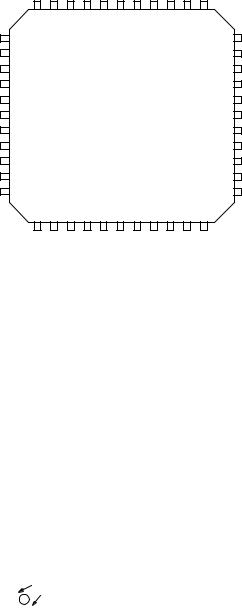
The MC68HC705C8A is available in six packages:
•40-pin plastic dual in-line package (PDIP)
•40-pin ceramic dual in-line package (cerdip)
•44-lead plastic-leaded chip carrier (PLCC)
•44-lead ceramic-leaded chip carrier (CLCC)
•44-pin quad flat pack (QFP)
•42-pin shrink dual in-line package (SDIP)
The pin assignments for these packages are shown in Figure 1-3,
Figure 1-4, Figure 1-5, and Figure 1-6.
|
|
|
|
|
1 |
40 |
|
|
VDD |
||
RESET |
|
|
|
|
|||||||
|
|
|
|
||||||||
|
|
|
|
|
2 |
39 |
|
|
OSC1 |
||
|
IRQ |
|
|
|
|
||||||
|
|
|
|
||||||||
VPP |
|
|
3 |
38 |
|
|
OSC2 |
||||
|
|
|
|
||||||||
PA7 |
|
|
4 |
37 |
|
|
TCAP |
||||
|
|
|
|
||||||||
PA6 |
|
5 |
36 |
|
|
PD7 |
|||||
|
|
|
|||||||||
PA5 |
|
6 |
35 |
|
|
TCMP |
|||||
|
|
|
|||||||||
|
|
|
|
7 |
34 |
|
|
PD5/ |
|
|
|
PA4 |
|
|
|
|
SS |
||||||
PA3 |
|
8 |
33 |
|
|
PD4/SCK |
|||||
|
|
|
|||||||||
PA2 |
|
9 |
32 |
|
|
PD3/MOSI |
|||||
|
|
|
|||||||||
PA1 |
|
10 |
31 |
|
|
PD2/MISO |
|||||
PA0 |
|
11 |
30 |
|
|
PD1/TDO |
|||||
PB0 |
|
12 |
29 |
|
|
PD0/RDI |
|||||
PB1 |
|
13 |
28 |
|
|
PC0 |
|||||
PB2 |
|
14 |
27 |
|
|
PC1 |
|||||
PB3 |
|
15 |
26 |
|
|
PC2 |
|||||
PB4 |
|
16 |
25 |
|
|
PC3 |
|||||
PB5 |
|
17 |
24 |
|
|
PC4 |
|||||
PB6 |
|
18 |
23 |
|
|
PC5 |
|||||
PB7 |
|
19 |
22 |
|
|
PC6 |
|||||
|
VSS |
|
20 |
21 |
|
|
PC7 |
||||
|
|
|
|||||||||
Figure 1-3. 40-Pin PDIP/Cerdip Pin Assignments
Technical Data |
|
MC68HC705C8A — Rev. 2.0 |
|
|
|
24 |
General Description |
MOTOROLA |
|
|
|
|
|
|
|
|
|
|
|
|
|
General Description |
||
|
|
|
|
|
|
|
|
|
|
|
|
|
|
Pin Assignments |
|
|
PA6 |
PA7 |
V |
NC |
IRQ |
|
RESET |
V |
OSC1 |
OSC2 |
TCAP |
NC |
|
|
|
|
|
|
|
|
|||||||||||
|
|
|
PP |
|
|
|
|
DD |
|
|
|
|
|
|
|
|
|
|
|
|
|
|
|
|
|
|
|
|
|
|
|
|
6 |
5 |
4 |
3 |
2 |
1 |
44 |
43 |
42 |
41 |
40 |
|
|
|
|
PA5 |
7 |
|
|
|
|
|
|
|
|
|
|
39 |
PD7 |
||
PA4 |
8 |
|
|
|
|
|
|
|
|
|
|
38 |
TCMP |
||
PA3 |
9 |
|
|
|
|
|
|
|
|
|
|
37 |
|
|
|
|
|
|
|
|
|
|
|
|
|
PD5/SS |
|
||||
PA2 |
10 |
|
|
|
|
|
|
|
|
|
|
36 |
PD4/SCK |
||
PA1 |
11 |
|
|
|
|
|
|
|
|
|
|
35 |
PD3/MOSI |
||
PA0 |
12 |
|
|
|
|
|
|
|
|
|
|
34 |
PD2/MISO |
||
PB0 |
13 |
|
|
|
|
|
|
|
|
|
|
33 |
PD1/TDO |
||
PB1 |
14 |
|
|
|
|
|
|
|
|
|
|
32 |
PD0/RDI |
||
PB2 |
15 |
|
|
|
|
|
|
|
|
|
|
31 |
PC0 |
||
PB3 |
16 |
|
|
|
|
|
|
|
|
|
|
30 |
PC1 |
||
PB4 |
17 |
|
|
|
|
|
|
|
|
|
|
29 |
PC2 |
||
|
18 |
19 |
20 |
21 |
22 |
23 |
24 |
25 |
26 |
27 |
28 |
|
|
|
|
|
NC |
PB5 |
PB6 |
PB7 |
SS |
|
NC |
PC7 |
PC6 |
PC5 |
PC4 |
PC3 |
|
|
|
|
V |
|
|
|
|
||||||||||
Figure 1-4. 44-Lead PLCC/CLCC Pin Assignments
|
|
|
|
|
TCMP |
|
PD5/SS |
PD4/SCK |
|
PD3/MOSI |
|
PD2/MISO |
|
PD1/TDO |
|
PD0/RDI |
|
PC0 |
|
PC1 |
|
PC2 |
|
PC3 |
|
|
|||
|
|
|
|
|
|
|
|
|
|
|
|
|
|
|
|
||||||||||||||
|
|
|
|
|
|
|
|
|
|
|
|
|
|
|
|
||||||||||||||
|
|
|
|
|
|
|
|
|
|
|
|
|
|
|
|
|
|
|
|
|
|
|
|
|
|
|
|
|
|
|
|
|
|
|
|
|
|
|
|
|
|
|
|
|
|
|
|
|
|
|
|
|
|
|
|
|
|
|
|
PD7 |
|
|
33 |
|
32 |
|
31 |
30 |
29 |
28 |
27 |
26 |
25 |
24 |
23 |
|
|
|
|||||||||||
|
|
34 |
|
|
|
|
|
|
|
|
|
|
|
|
|
|
|
|
|
|
|
22 |
|
NC |
|||||
TCAP |
|
|
35 |
|
|
|
|
|
|
|
|
|
|
|
|
|
|
|
|
|
|
|
21 |
|
PC4 |
||||
|
|
|
|
|
|
|
|
|
|
|
|
|
|
|
|
|
|
|
|
|
|||||||||
OSC2 |
|
|
36 |
|
|
|
|
|
|
|
|
|
|
|
|
|
|
|
|
|
|
|
20 |
|
PC5 |
||||
|
|
|
|
|
|
|
|
|
|
|
|
|
|
|
|
|
|
|
|
|
|||||||||
OSC1 |
|
|
37 |
|
|
|
|
|
|
|
|
|
|
|
|
|
|
|
|
|
|
|
19 |
|
PC6 |
||||
|
|
|
|
|
|
|
|
|
|
|
|
|
|
|
|
|
|
|
|
|
|||||||||
VDD |
|
|
38 |
|
|
|
|
|
|
|
|
|
|
|
|
|
|
|
|
|
|
|
18 |
|
PC7 |
||||
|
|
|
|
|
|
|
|
|
|
|
|
|
|
|
|
|
|
|
|
|
|||||||||
|
|
|
|
|
|
|
|
|
|
|
|
|
|
|
|
|
|
|
|
|
|||||||||
|
NC |
|
|
39 |
|
|
|
|
|
|
|
|
|
|
|
|
|
|
|
|
|
|
|
17 |
|
VSS |
|||
|
|
|
|
|
|
|
|
|
|
|
|
|
|
|
|
|
|
|
|
|
|
||||||||
|
NC |
|
|
40 |
|
|
|
|
|
|
|
|
|
|
|
|
|
|
|
|
|
|
|
16 |
|
NC |
|||
|
|
|
|
41 |
|
|
|
|
|
|
|
|
|
|
|
|
|
|
|
|
|
|
|
15 |
|
PB7 |
|||
RESET |
|
|
|
|
|
|
|
|
|
|
|
|
|
|
|
|
|
|
|
|
|
||||||||
|
|
|
|
42 |
|
|
|
|
|
|
|
|
|
|
|
|
|
|
|
|
|
|
|
14 |
|
PB6 |
|||
|
IRQ |
|
|
|
|
|
|
|
|
|
|
|
|
|
|
|
|
|
|
|
|
|
|||||||
VPP |
|
|
43 |
|
|
|
|
|
|
|
|
|
|
|
|
|
|
|
|
|
|
|
13 |
|
PB5 |
||||
|
|
|
|
|
|
|
|
|
|
|
|
|
|
|
|
|
|
|
|
|
|||||||||
|
PA7 |
|
|
44 |
1 |
|
|
|
|
|
|
|
|
|
|
|
|
|
|
|
|
|
12 |
|
PB4 |
||||
|
|
|
|
|
|
|
|
|
|
|
|
|
|
|
|
|
|
|
|
|
|
|
|
||||||
|
|
|
|
|
|
|
2 |
|
3 |
4 |
5 |
6 |
7 |
8 |
9 |
10 |
11 |
|
|
|
|||||||||
|
|
|
|
|
|
|
|
|
|
|
|
|
|
|
|
|
|
|
|
|
|
|
|
|
|
|
|
|
|
|
|
|
|
|
PA6 |
|
PA5 |
PA4 |
|
PA3 |
|
PA2 |
|
PA1 |
|
PA0 |
|
PB0 |
|
PB1 |
|
PB2 |
|
PB3 |
|
|
|||
Figure 1-5. 44-Pin QFP Pin Assignments
MC68HC705C8A — Rev. 2.0 |
|
Technical Data |
|
|
|
MOTOROLA |
General Description |
25 |

General Description
|
|
|
|
|
|
1 |
42 |
|
VDD |
||
RESET |
|
|
|
||||||||
|
|
|
|
|
|
2 |
41 |
|
OSC1 |
||
|
IRQ |
|
|
|
|||||||
|
|
|
|
|
|
|
|
|
|
|
|
|
VPP |
|
3 |
40 |
|
OSC2 |
|||||
|
|
|
|
|
|
|
|
|
|
|
|
|
PA7 |
|
4 |
39 |
|
TCAP |
|||||
|
|
|
|
|
|
|
|
|
|
|
|
|
|
|
|
|
|
|
|
|
|
|
|
|
PA6 |
|
5 |
38 |
|
PD7 |
|||||
|
|
|
|
|
|
|
|
|
|
|
|
|
|
|
|
|
|
|
|
|
|
|
|
|
PA5 |
|
6 |
37 |
|
TCMP |
|||||
|
|
|
|
|
|
|
|
|
|
|
|
|
|
|
|
|
|
|
|
|
|
|
|
|
PA4 |
|
7 |
36 |
|
PD5/SS |
|
||||
|
|
|
|
|
|
|
|
|
|
|
|
|
PA3 |
|
8 |
35 |
|
PD4/SCK |
|||||
|
|
|
|
|
|
|
|
|
|
|
|
|
|
|
|
|
|
|
|
|
|
|
|
|
PA2 |
|
9 |
34 |
|
PD3/MOSI |
|||||
|
|
|
|
|
|
|
|
|
|
|
|
|
|
|
|
|
|
|
|
|
|
|
|
|
PA1 |
|
10 |
33 |
|
PD2/MISO |
|||||
|
|
|
|
|
|
|
|
|
|
|
|
|
|
|
|
|
|
|
|
|
|
|
|
|
PA0 |
|
11 |
32 |
|
PD1/TDO |
|||||
|
|
|
|
|
|
|
|
|
|
|
|
|
|
|
|
|
|
|
|
|
|
|
|
|
PB0 |
|
12 |
31 |
|
PD0/RDI |
|||||
|
|
|
|
|
|
|
|
|
|
|
|
|
|
|
|
|
|
|
|
|
|
|
|
|
PB1 |
|
13 |
30 |
|
PC0 |
|||||
|
|
|
|
|
|
|
|
|
|
|
|
|
PB2 |
|
14 |
29 |
|
PC1 |
|||||
|
|
|
|
|
|
|
|
|
|
|
|
|
|
|
|
|
|
|
|
|
|
|
|
|
PB3 |
|
15 |
28 |
|
PC2 |
|||||
|
|
|
|
|
|
|
|
|
|
|
|
|
|
|
|
|
|
|
|
|
|
|
|
|
NC |
|
16 |
27 |
|
NC |
|||||
|
|
|
|
|
|
|
|
|
|
|
|
|
|
|
|
|
|
|
|
|
|
|
|
|
PB4 |
|
17 |
26 |
|
PC3 |
|||||
|
|
|
|
|
|
|
|
|
|
|
|
|
|
|
|
|
|
|
|
|
|
|
|
|
PB5 |
|
18 |
25 |
|
PC4 |
|||||
|
|
|
|
|
|
|
|
|
|
|
|
PB6 |
|
19 |
24 |
|
PC5 |
||||||
|
|
|
|
|
|
20 |
23 |
|
PC6 |
||
|
|
|
|
|
|
|
|||||
PB7 |
|
|
|||||||||
|
|
|
|
|
21 |
22 |
|
PC7 |
|||
|
VSS |
|
|
|
|||||||
|
|
|
|
|
|
|
|
|
|
|
|
Figure 1-6. 42-Pin SDIP Pin Assignments
Technical Data |
|
MC68HC705C8A — Rev. 2.0 |
|
|
|
26 |
General Description |
MOTOROLA |

General Description
Pin Functions
1.7 Pin Functions
This subsection describes the MC68HC705C8A signals. Reference is made, where applicable, to other sections that contain more detail about the function being performed.
1.7.1 VDD and VSS
VDD and VSS are the power supply and ground pins. The MCU operates from a single power supply.
Very fast signal transitions occur on the MCU pins, placing high short-duration current demands on the power supply. To prevent noise problems, take special care to provide good power supply bypassing at the MCU. Place bypass capacitors as close to the MCU as possible, as shown in
Figure 1-7.
1.7.2 OSC1 and OSC2
V+
VDD
|
|
+ |
MCU |
C1 |
C2 |
VSS
Figure 1-7. Bypassing Layout
Recommendation
The OSC1 and OSC2 pins are the control connections for the 2-pin on-chip oscillator. The oscillator can be driven by:
•Crystal resonator
•Ceramic resonator
•External clock signal
NOTE: The frequency of the internal oscillator is fOSC. The MCU divides the internal oscillator output by two to produce the internal clock with a frequency of fOP.
MC68HC705C8A — Rev. 2.0 |
|
Technical Data |
|
|
|
MOTOROLA |
General Description |
27 |
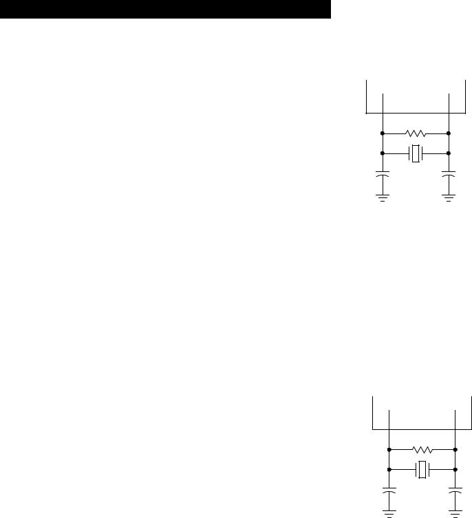
General Description
1.7.2.1 Crystal Resonator
The circuit in Figure 1-8 shows a crystal oscillator circuit for an AT-cut, parallel resonant crystal. Follow the crystal supplier’s recommendations, because the crystal parameters determine the external component values required to provide reliable startup and maximum stability. The load capacitance values used in the oscillator circuit design should account for all stray layout capacitances. To minimize output distortion, mount the crystal and capacitors as close as possible to the pins.
|
MCU |
|
OSC1 |
10 MΩ |
OSC2 |
22 pF |
XTAL |
22 pF |
2 MHz |
Starting value only. Follow crystal supplier’s recommendations regarding component values that will provide reliable startup and maximum stability.
Figure 1-8. Crystal
Connections
NOTE: Use an AT-cut crystal and not a strip or tuning fork crystal. The MCU might overdrive or have the incorrect characteristic impedance for a strip or tuning fork crystal.
1.7.2.2 Ceramic Resonator
To reduce cost, use a ceramic |
|
MCU |
|
resonator instead of a crystal. Use the |
|
|
|
circuit shown in Figure 1-9 for a 2-pin |
|
|
|
ceramic resonator or the circuit shown |
OSC1 |
R |
OSC2 |
in Figure 1-10 for a 3-pin ceramic |
|
|
|
resonator, and follow the resonator |
|
|
|
manufacturer’s recommendations. |
|
CERAMIC |
|
|
C |
RESONATOR |
C |
The external component values required for maximum stability and reliable starting depend upon the resonator parameters. The load
capacitance values used in the oscillator circuit design should include all stray layout capacitances. To minimize output distortion, mount the resonator and capacitors as close as possible to the pins.
Technical Data |
|
MC68HC705C8A — Rev. 2.0 |
|
|
|
28 |
General Description |
MOTOROLA |

General Description
Pin Functions
MCU
OSC1 |
|
OSC2 |
|
|
|
|
|
|
CERAMIC
 RESONATOR
Figure 1-10. 3-Pin
Ceramic Resonator
Connections
NOTE: The bus frequency (fOP) is one-half the external or crystal frequency
(fOSC), while the processor clock cycle (tCYC) is two times the fOSC period.
1.7.2.3 External Clock Signal
An external clock from another CMOS-compatible device can drive the OSC1 input, with the OSC2 pin unconnected, as Figure 1-11 shows.
|
MCU |
OSC1 |
OSC2 |
EXTERNAL
CMOS CLOCK
Figure 1-11. External
Clock
NOTE: The bus frequency (fOP) is one-half the external frequency (fOSC) while the processor clock cycle is two times the fOSC period.
MC68HC705C8A — Rev. 2.0 |
|
Technical Data |
|
|
|
MOTOROLA |
General Description |
29 |

General Description
1.7.3 External Reset Pin (RESET)
A logic 0 on the bidirectional RESET pin forces the MCU to a known startup state. The RESET pin contains an internal Schmitt trigger as part of its input to improve noise immunity. See Section 5. Resets.
1.7.4 External Interrupt Request Pin (IRQ)
The IRQ pin is an asynchronous external interrupt pin. The IRQ pin contains an internal Schmitt trigger as part of its input to improve noise immunity. See 4.3.2 External Interrupt (IRQ).
1.7.5 Input Capture Pin (TCAP)
The TCAP pin is the input capture pin for the on-chip capture/compare timer. The TCAP pin contains an internal Schmitt trigger as part of its input to improve noise immunity. See Section 8. Capture/Compare Timer.
1.7.6 Output Compare Pin (TCMP)
The TCMP pin is the output compare pin for the on-chip capture/compare timer. See Section 8. Capture/Compare Timer.
1.7.7 Port A I/O Pins (PA7–PA0)
These eight I/O lines comprise port A, a general-purpose, bidirectional
I/O port. The pins are programmable as either inputs or outputs under software control of the data direction registers. See 7.3 Port A.
1.7.8 Port B I/O Pins (PB7–PB0)
These eight I/O pins comprise port B, a general-purpose, bidirectional I/O port. The pins are programmable as either inputs or outputs under software control of the data direction registers. Port B pins also can be configured to function as external interrupts. See 7.4 Port B.
Technical Data |
|
MC68HC705C8A — Rev. 2.0 |
|
|
|
30 |
General Description |
MOTOROLA |
Loading...