


 Loading...
MOTOROLA MC68HC908QY4, MC68HC908QT4, MC68HC908QY2, MC68HC908QT2, MC68HC908QY1 Technical data
...MC68HC908QY4
MC68HC908QT4
MC68HC908QY2
MC68HC908QT2
MC68HC908QY1
MC68HC908QT1
Data Sheet
M68HC08
Microcontrollers
MC68HC908QY4/D Rev 3.0
1/2004
MOTOROLA.COM/SEMICONDUCTORS

MC68HC908QY4
MC68HC908QT4
MC68HC908QY2
MC68HC908QT2
MC68HC908QY1
MC68HC908QT1
Data Sheet
To provide the most up-to-date information, the revision of our documents on the World Wide Web will be the most current. Your printed copy may be an earlier revision. To verify you have the latest information available, refer to:
http://motorola.com/semiconductors/
The following revision history table summarizes changes contained in this document. For your convenience, the page number designators have been linked to the appropriate location.
Motorola and the Stylized M Logo are registered trademarks of Motorola, Inc. |
|
DigitalDNA is a trademark of Motorola, Inc. |
|
This product incorporates SuperFlash® technol ogy licensed from SST. |
© Motorola, Inc., 2004 |
MC68HC908QY/QT Family — Rev. 3 |
Data Sheet |
|
|
|
|
MOTOROLA |
3 |

Revision History
|
|
Revision History |
|
|
|
|
|
|
|
Date |
Revision |
Description |
Page |
|
Level |
Number(s) |
|||
|
|
|||
|
|
|
|
|
September, |
N/A |
Initial release |
N/A |
|
2002 |
||||
|
|
|
||
|
|
|
|
|
|
|
1.2 Features — Added 8-pin dual flat no lead (DFN) packages to features list. |
19 |
|
|
|
|
|
|
|
|
Figure 1-2. MCU Pin Assignments — Figure updated to include DFN |
21 |
|
|
|
packages. |
||
|
|
|
||
|
|
|
|
|
|
|
Figure 2-1. Memory Map — Clarified illegal address and unimplemented |
28 |
|
|
|
memory. |
||
|
|
|
||
|
|
|
|
|
|
|
Figure 2-2. Control, Status, and Data Registers — Corrected bit definitions |
28 |
|
|
|
for Port A Data Register (PTA) and Data Direction Register A (DDRA). |
||
|
|
|
||
|
|
|
|
|
|
|
Table 13-3. Interrupt Sources — Corrected vector addresses for keyboard |
124 |
|
|
|
interrupt and ADC conversion complete interrupt. |
||
|
|
|
||
|
|
|
|
|
|
|
Section 13. System Integration Module (SIM) — Removed reference to break |
113 |
|
|
|
status register as it is duplicated in break module. |
||
|
|
|
||
|
|
|
|
|
|
|
11.3.1 Internal Oscillator and 11.3.1.1 Internal Oscillator Trimming — |
|
|
|
|
Clarified oscillator trim option ordering information and what to expect with |
97 |
|
|
|
untrimmed device. |
|
|
|
|
|
|
|
|
|
Figure 11-5. Oscillator Trim Register (OSCTRIM) — Bit 1 designation |
104 |
|
|
|
corrected. |
||
|
|
|
||
|
|
|
|
|
December, |
|
Figure 15-13. Monitor Mode Circuit (Internal Clock, No High Voltage) — |
160 |
|
0.1 |
Diagram updated for clarity. |
|||
2002 |
|
|||
|
|
|
||
|
|
Figure 12-1. I/O Port Register Summary — Corrected bit definitions for PTA7, |
105 |
|
|
|
DDRA7, and DDRA6. |
||
|
|
|
||
|
|
|
|
|
|
|
Figure 12-2. Port A Data Register (PTA) — Corrected bit defi nition for PTA7. |
106 |
|
|
|
|
|
|
|
|
Figure 12-3. Data Direction Register A (DDRA) — Corrected bit definitions for |
107 |
|
|
|
DDRA7 and DDRA6. |
||
|
|
|
||
|
|
|
|
|
|
|
Figure 12-6. Port B Data Register (PTB) — Corrected bit de finition for PTB1 |
109 |
|
|
|
|
|
|
|
|
Section 9. Keyboard Interrupt Module (KBI) — Section reworked after |
83 |
|
|
|
deletion of auto wakeup for clarity. |
||
|
|
|
||
|
|
|
|
|
|
|
Section 4. Auto Wakeup Module (AWU) — New section added for clarity. |
49 |
|
|
|
|
|
|
|
|
Figure 10-1. LVI Module Block Diagram — Corrected LVI stop representation. |
91 |
|
|
|
|
|
|
|
|
Section 16. Electrical Specifications — Extensive changes made to electrical |
169 |
|
|
|
specifications. |
||
|
|
|
||
|
|
|
|
|
|
|
17.5 8-Pin Dual Flat No Lead (DFN) Package (Case #1452) — Added case |
187 |
|
|
|
outline drawing for DFN package. |
||
|
|
|
||
|
|
|
|
|
|
|
Section 17. Ordering Information and Mechanical Specifications — Added |
185 |
|
|
|
ordering information for DFN package. |
||
|
|
|
||
|
|
|
|
|
January, |
0.2 |
4.2 Features — Corrected third bulleted item. |
49 |
|
2003 |
||||
|
|
|
||
|
|
|
|
Data Sheet |
MC68HC908QY/QT Family — Rev. 3 |
|
|
4 |
Revision History |
MOTOROLA |

Revision History
Revision History (Continued)
Date |
Revision |
Description |
Page |
|
Level |
Number(s) |
|||
|
|
|||
|
|
|
|
|
|
|
Reformatted to meet latest M68HC08 documentation standards |
N/A |
|
|
|
|
|
|
|
|
Figure 1-1. Block Diagram — Diagram redrawn to include keyboard interrupt |
20 |
|
|
|
module and TCLK pin designator. |
||
|
|
|
||
|
|
|
|
|
|
|
Figure 1-2. MCU Pin Assignments — Added TCLK pin designator. |
21 |
|
|
|
|
|
|
|
|
Table 1-2. Pin Functions — Added TCLK pin description. |
22 |
|
|
|
|
|
|
|
|
Table 1-3. Function Priority in Shared Pins — Revised table for clarity and to |
23 |
|
|
|
add TCLK. |
||
|
|
|
||
|
|
|
|
|
|
|
Figure 2-1. Memory Map — Corrected names for the IRQ status and control |
26 |
|
|
|
register (INTSCR) bits 3–0. |
||
August, |
|
|
||
1.0 |
|
|
||
2003 |
3.7.3 ADC Input Clock Register — Clarified bit description for the ADC clock |
48 |
||
|
||||
|
|
prescaler bits. |
||
|
|
|
||
|
|
|
|
|
|
|
4.3 Functional Description — Updated periodic wakeup request values. |
51 |
|
|
|
|
|
|
|
|
Figure 6-1. COP Block Diagram — Reworked for clarity |
59 |
|
|
|
|
|
|
|
|
Section 8. External Interrupt (IRQ) — Corrected bit names for MODE, IRQF, |
77–81 |
|
|
|
ACK, and IMASK |
||
|
|
|
||
|
|
|
|
|
|
|
Section 14. Timer Interface Module (TIM) — Added TCLK function. |
131–147 |
|
|
|
|
|
|
|
|
15.3 Monitor Module (MON) — Updated with additional data. |
156 |
|
|
|
|
|
|
|
|
Section 16. Electrical Specifications — Updated with additional data. |
169–183 |
|
|
|
|
|
|
|
|
Figure 2-2. Control, Status, and Data Registers — Deleted unimplemented |
|
|
|
|
areas from $FFB0–$FFBD and $FFC2–$FFCF as they are actually available. |
28 |
|
|
|
Also corrected $FFBF designation from unimplemented to reserved. |
|
|
|
|
|
|
|
|
|
Figure 6-1. COP Block Diagram — Reworked for clarity |
59 |
|
|
|
|
|
|
|
|
6.3.2 STOP Instruction — Added subsection |
60 |
|
|
|
|
|
|
|
|
13.4.2 Active Resets from Internal Sources — Reworked notes for clarity. |
117 |
|
|
|
|
|
|
October, |
2.0 |
Table 13-2. Reset Recovery Timing — Replaced previous table with new |
118 |
|
2003 |
information. |
|||
|
|
|||
|
|
|
|
|
|
|
Section 14. Timer Interface Module (TIM) — Updated with additional data. |
131 |
|
|
|
|
|
|
|
|
Figure 15-3. Break I/O Register Summary — Corrected bit designators for the |
151 |
|
|
|
BRKAR register |
||
|
|
|
||
|
|
|
|
|
|
|
15.3 Monitor Module (MON) — Clarified seventh bullet. |
156 |
|
|
|
|
|
|
|
|
Table 17-1. MC Order Numbers — Corrected temperature and package |
185 |
|
|
|
designators. |
||
|
|
|
||
|
|
|
|
|
|
|
Figure 2-2. Control, Status, and Data Registers — Corrected reset state for |
|
|
January, |
|
the FLASH Block Protect Register at address location $FFBE and the Internal |
32 |
|
3.0 |
Oscillator Trim Value at $FFC0. |
|
||
2004 |
|
|
||
|
Figure 2-5. FLASH Block Protect Register (FLBPR) — Restated reset state |
39 |
||
|
|
|||
|
|
for clarity. |
||
|
|
|
||
|
|
|
|
|
MC68HC908QY/QT Family — Rev. 3 |
Data Sheet |
|||
|
|
|
|
|
|
|
|
|
|
MOTOROLA |
Revision History |
5 |

Revision History
Data Sheet |
MC68HC908QY/QT Family — Rev. 3 |
|
|
6 |
Revision History |
MOTOROLA |

Data Sheet — MC68HC908QY/QT Family
List of Sections
Section 1. General Description . . . . . . . . . . . . . . . . . . . . . . . . . . . . . . . 17 Section 2. Memory . . . . . . . . . . . . . . . . . . . . . . . . . . . . . . . . . . . . . . . . . 25 Section 3. Analog-to-Digital Converter (ADC) . . . . . . . . . . . . . . . . . . . 41 Section 4. Auto Wakeup Module (AWU) . . . . . . . . . . . . . . . . . . . . . . . . 49 Section 5. Configuration Register (CONFIG) . . . . . . . . . . . . . . . . . . . . 55 Section 6. Computer Operating Properly (COP) . . . . . . . . . . . . . . . . . 59 Section 7. Central Processor Unit (CPU) . . . . . . . . . . . . . . . . . . . . . . . 63 Section 8. External Interrupt (IRQ) . . . . . . . . . . . . . . . . . . . . . . . . . . . . 77 Section 9. Keyboard Interrupt Module (KBI) . . . . . . . . . . . . . . . . . . . . 83 Section 10. Low-Voltage Inhibit (LVI) . . . . . . . . . . . . . . . . . . . . . . . . . . 91 Section 11. Oscillator Module (OSC). . . . . . . . . . . . . . . . . . . . . . . . . . . 95 Section 12. Input/Output Ports (PORTS) . . . . . . . . . . . . . . . . . . . . . . 105 Section 13. System Integration Module (SIM) . . . . . . . . . . . . . . . . . . 113 Section 14. Timer Interface Module (TIM) . . . . . . . . . . . . . . . . . . . . . . 131 Section 15. Development Support. . . . . . . . . . . . . . . . . . . . . . . . . . . . 149 Section 16. Electrical Specifications. . . . . . . . . . . . . . . . . . . . . . . . . . 169
Section 17. Ordering Information and Mechanical
Specifications . . . . . . . . . . . . . . . . . . . . . . . . . . . . . . . . . 185
MC68HC908QY/QT Family — Rev. 3 |
Data Sheet |
|
|
MOTOROLA |
List of Sections |
7 |

List of Sections
Data Sheet |
MC68HC908QY/QT Family — Rev. 3 |
|
|
8 |
List of Sections |
MOTOROLA |

Data Sheet — MC68HC908QY/QT Family
Table of Contents
Section 1. General Description
1.1 Introduction. . . . . . . . . . . . . . . . . . . . . . . . . . . . . . . . . . . . . . . . . . . . . . . 17
1.2 Features . . . . . . . . . . . . . . . . . . . . . . . . . . . . . . . . . . . . . . . . . . . . . . . . . 17
1.3 MCU Block Diagram . . . . . . . . . . . . . . . . . . . . . . . . . . . . . . . . . . . . . . . . 19
1.4 Pin Assignments. . . . . . . . . . . . . . . . . . . . . . . . . . . . . . . . . . . . . . . . . . . 19
1.5 Pin Functions . . . . . . . . . . . . . . . . . . . . . . . . . . . . . . . . . . . . . . . . . . . . . 22
1.6 Pin Function Priority . . . . . . . . . . . . . . . . . . . . . . . . . . . . . . . . . . . . . . . . 23
Section 2. Memory
2.1 Introduction. . . . . . . . . . . . . . . . . . . . . . . . . . . . . . . . . . . . . . . . . . . . . . . 25
2.2 Unimplemented Memory Locations . . . . . . . . . . . . . . . . . . . . . . . . . . . . 25
2.3 Reserved Memory Locations . . . . . . . . . . . . . . . . . . . . . . . . . . . . . . . . . 25
2.4 Input/Output (I/O) Section. . . . . . . . . . . . . . . . . . . . . . . . . . . . . . . . . . . . 27
2.5 Random-Access Memory (RAM) . . . . . . . . . . . . . . . . . . . . . . . . . . . . . . 33
2.6 FLASH Memory (FLASH) . . . . . . . . . . . . . . . . . . . . . . . . . . . . . . . . . . . . 34
2.6.1 FLASH Control Register . . . . . . . . . . . . . . . . . . . . . . . . . . . . . . . . . . 34
2.6.2 FLASH Page Erase Operation . . . . . . . . . . . . . . . . . . . . . . . . . . . . . 35
2.6.3 FLASH Mass Erase Operation . . . . . . . . . . . . . . . . . . . . . . . . . . . . . 36
2.6.4 FLASH Program Operation. . . . . . . . . . . . . . . . . . . . . . . . . . . . . . . . 36
2.6.5 FLASH Protection . . . . . . . . . . . . . . . . . . . . . . . . . . . . . . . . . . . . . . . 37
2.6.6 FLASH Block Protect Register . . . . . . . . . . . . . . . . . . . . . . . . . . . . . 39
2.6.7 Wait Mode. . . . . . . . . . . . . . . . . . . . . . . . . . . . . . . . . . . . . . . . . . . . . 40
2.6.8 Stop Mode . . . . . . . . . . . . . . . . . . . . . . . . . . . . . . . . . . . . . . . . . . . . 40
Section 3. Analog-to-Digital Converter (ADC)
3.1 Introduction. . . . . . . . . . . . . . . . . . . . . . . . . . . . . . . . . . . . . . . . . . . . . . . 41
3.2 Features . . . . . . . . . . . . . . . . . . . . . . . . . . . . . . . . . . . . . . . . . . . . . . . . . 41
3.3 Functional Description . . . . . . . . . . . . . . . . . . . . . . . . . . . . . . . . . . . . . . 43
3.3.1 ADC Port I/O Pins. . . . . . . . . . . . . . . . . . . . . . . . . . . . . . . . . . . . . . . 44
3.3.2 Voltage Conversion . . . . . . . . . . . . . . . . . . . . . . . . . . . . . . . . . . . . . 44
3.3.3 Conversion Time. . . . . . . . . . . . . . . . . . . . . . . . . . . . . . . . . . . . . . . . 44
3.3.4 Continuous Conversion . . . . . . . . . . . . . . . . . . . . . . . . . . . . . . . . . . 44
3.3.5 Accuracy and Precision . . . . . . . . . . . . . . . . . . . . . . . . . . . . . . . . . . 44
3.4 Interrupts . . . . . . . . . . . . . . . . . . . . . . . . . . . . . . . . . . . . . . . . . . . . . . . . 45
MC68HC908QY/QT Family — Rev. 3 |
Data Sheet |
|
|
MOTOROLA |
Table of Contents |
9 |

Table of Contents
3.5 Low-Power Modes . . . . . . . . . . . . . . . . . . . . . . . . . . . . . . . . . . . . . . . . . 45
3.5.1 Wait Mode. . . . . . . . . . . . . . . . . . . . . . . . . . . . . . . . . . . . . . . . . . . . . 45
3.5.2 Stop Mode . . . . . . . . . . . . . . . . . . . . . . . . . . . . . . . . . . . . . . . . . . . . 45
3.6 Input/Output Signals . . . . . . . . . . . . . . . . . . . . . . . . . . . . . . . . . . . . . . . . 45
3.7 Input/Output Registers . . . . . . . . . . . . . . . . . . . . . . . . . . . . . . . . . . . . . . 45
3.7.1 ADC Status and Control Register . . . . . . . . . . . . . . . . . . . . . . . . . . . 46
3.7.2 ADC Data Register . . . . . . . . . . . . . . . . . . . . . . . . . . . . . . . . . . . . . . 47
3.7.3 ADC Input Clock Register. . . . . . . . . . . . . . . . . . . . . . . . . . . . . . . . . 48
Section 4. Auto Wakeup Module (AWU)
4.1 Introduction. . . . . . . . . . . . . . . . . . . . . . . . . . . . . . . . . . . . . . . . . . . . . . . 49
4.2 Features . . . . . . . . . . . . . . . . . . . . . . . . . . . . . . . . . . . . . . . . . . . . . . . . . 49
4.3 Functional Description . . . . . . . . . . . . . . . . . . . . . . . . . . . . . . . . . . . . . . 50
4.4 Wait Mode . . . . . . . . . . . . . . . . . . . . . . . . . . . . . . . . . . . . . . . . . . . . . . . 51
4.5 Stop Mode . . . . . . . . . . . . . . . . . . . . . . . . . . . . . . . . . . . . . . . . . . . . . . . 51
4.6 Input/Output Registers . . . . . . . . . . . . . . . . . . . . . . . . . . . . . . . . . . . . . . 51
4.6.1 Port A I/O Register . . . . . . . . . . . . . . . . . . . . . . . . . . . . . . . . . . . . . . 52
4.6.2 Keyboard Status and Control Register . . . . . . . . . . . . . . . . . . . . . . . 52
4.6.3 Keyboard Interrupt Enable Register . . . . . . . . . . . . . . . . . . . . . . . . . 53
Section 5. Configuration Register (CONFIG)
5.1 Introduction. . . . . . . . . . . . . . . . . . . . . . . . . . . . . . . . . . . . . . . . . . . . . . . 55
5.2 Functional Description . . . . . . . . . . . . . . . . . . . . . . . . . . . . . . . . . . . . . . 55
Section 6. Computer Operating Properly (COP)
6.1 Introduction. . . . . . . . . . . . . . . . . . . . . . . . . . . . . . . . . . . . . . . . . . . . . . . 59
6.2 Functional Description . . . . . . . . . . . . . . . . . . . . . . . . . . . . . . . . . . . . . . 59
6.3 I/O Signals . . . . . . . . . . . . . . . . . . . . . . . . . . . . . . . . . . . . . . . . . . . . . . . 60
6.3.1 BUSCLKX4 . . . . . . . . . . . . . . . . . . . . . . . . . . . . . . . . . . . . . . . . . . . . 60
6.3.2 STOP Instruction . . . . . . . . . . . . . . . . . . . . . . . . . . . . . . . . . . . . . . . 60
6.3.3 COPCTL Write . . . . . . . . . . . . . . . . . . . . . . . . . . . . . . . . . . . . . . . . . 60
6.3.4 Power-On Reset . . . . . . . . . . . . . . . . . . . . . . . . . . . . . . . . . . . . . . . . 60
6.3.5 Internal Reset . . . . . . . . . . . . . . . . . . . . . . . . . . . . . . . . . . . . . . . . . . 60
6.3.6 COPD (COP Disable) . . . . . . . . . . . . . . . . . . . . . . . . . . . . . . . . . . . . 61
6.3.7 COPRS (COP Rate Select) . . . . . . . . . . . . . . . . . . . . . . . . . . . . . . . 61
6.4 COP Control Register . . . . . . . . . . . . . . . . . . . . . . . . . . . . . . . . . . . . . . . 61
6.5 Interrupts . . . . . . . . . . . . . . . . . . . . . . . . . . . . . . . . . . . . . . . . . . . . . . . . 61
6.6 Monitor Mode . . . . . . . . . . . . . . . . . . . . . . . . . . . . . . . . . . . . . . . . . . . . . 61
6.7 Low-Power Modes . . . . . . . . . . . . . . . . . . . . . . . . . . . . . . . . . . . . . . . . . 61
6.7.1 Wait Mode. . . . . . . . . . . . . . . . . . . . . . . . . . . . . . . . . . . . . . . . . . . . . 61
6.7.2 Stop Mode . . . . . . . . . . . . . . . . . . . . . . . . . . . . . . . . . . . . . . . . . . . . 62
6.8 COP Module During Break Mode . . . . . . . . . . . . . . . . . . . . . . . . . . . . . . 62
Data Sheet |
MC68HC908QY/QT Family — Rev. 3 |
|
|
10 |
Table of Contents |
MOTOROLA |
Table of Contents
Section 7. Central Processor Unit (CPU)
7.1 Introduction. . . . . . . . . . . . . . . . . . . . . . . . . . . . . . . . . . . . . . . . . . . . . . . 63
7.2 Features . . . . . . . . . . . . . . . . . . . . . . . . . . . . . . . . . . . . . . . . . . . . . . . . . 63
7.3 CPU Registers . . . . . . . . . . . . . . . . . . . . . . . . . . . . . . . . . . . . . . . . . . . . 64
7.3.1 Accumulator . . . . . . . . . . . . . . . . . . . . . . . . . . . . . . . . . . . . . . . . . . . 64
7.3.2 Index Register. . . . . . . . . . . . . . . . . . . . . . . . . . . . . . . . . . . . . . . . . . 65
7.3.3 Stack Pointer . . . . . . . . . . . . . . . . . . . . . . . . . . . . . . . . . . . . . . . . . . 65
7.3.4 Program Counter . . . . . . . . . . . . . . . . . . . . . . . . . . . . . . . . . . . . . . . 66
7.3.5 Condition Code Register. . . . . . . . . . . . . . . . . . . . . . . . . . . . . . . . . . 66
7.4 Arithmetic/Logic Unit (ALU) . . . . . . . . . . . . . . . . . . . . . . . . . . . . . . . . . . 68
7.5 Low-Power Modes . . . . . . . . . . . . . . . . . . . . . . . . . . . . . . . . . . . . . . . . . 68
7.5.1 Wait Mode. . . . . . . . . . . . . . . . . . . . . . . . . . . . . . . . . . . . . . . . . . . . . 68
7.5.2 Stop Mode . . . . . . . . . . . . . . . . . . . . . . . . . . . . . . . . . . . . . . . . . . . . 68
7.6 CPU During Break Interrupts . . . . . . . . . . . . . . . . . . . . . . . . . . . . . . . . . 68
7.7 Instruction Set Summary . . . . . . . . . . . . . . . . . . . . . . . . . . . . . . . . . . . . 69
7.8 Opcode Map . . . . . . . . . . . . . . . . . . . . . . . . . . . . . . . . . . . . . . . . . . . . . . 75
Section 8. External Interrupt (IRQ)
8.1 Introduction. . . . . . . . . . . . . . . . . . . . . . . . . . . . . . . . . . . . . . . . . . . . . . . 77
8.2 Features . . . . . . . . . . . . . . . . . . . . . . . . . . . . . . . . . . . . . . . . . . . . . . . . . 77
8.3 Functional Description . . . . . . . . . . . . . . . . . . . . . . . . . . . . . . . . . . . . . . 77
8.4 IRQ Pin . . . . . . . . . . . . . . . . . . . . . . . . . . . . . . . . . . . . . . . . . . . . . . . . . . 80
8.5 IRQ Module During Break Interrupts . . . . . . . . . . . . . . . . . . . . . . . . . . . 81
8.6 IRQ Status and Control Register . . . . . . . . . . . . . . . . . . . . . . . . . . . . . . 81
Section 9. Keyboard Interrupt Module (KBI)
9.1 Introduction. . . . . . . . . . . . . . . . . . . . . . . . . . . . . . . . . . . . . . . . . . . . . . . 83
9.2 Features . . . . . . . . . . . . . . . . . . . . . . . . . . . . . . . . . . . . . . . . . . . . . . . . . 83
9.3 Functional Description . . . . . . . . . . . . . . . . . . . . . . . . . . . . . . . . . . . . . . 85
9.3.1 Keyboard Operation . . . . . . . . . . . . . . . . . . . . . . . . . . . . . . . . . . . . . 85
9.3.2 Keyboard Initialization. . . . . . . . . . . . . . . . . . . . . . . . . . . . . . . . . . . . 87
9.4 Wait Mode . . . . . . . . . . . . . . . . . . . . . . . . . . . . . . . . . . . . . . . . . . . . . . . 87
9.5 Stop Mode . . . . . . . . . . . . . . . . . . . . . . . . . . . . . . . . . . . . . . . . . . . . . . . 87
9.6 Keyboard Module During Break Interrupts . . . . . . . . . . . . . . . . . . . . . . . 87
9.7 Input/Output Registers . . . . . . . . . . . . . . . . . . . . . . . . . . . . . . . . . . . . . . 88
9.7.1 Keyboard Status and Control Register . . . . . . . . . . . . . . . . . . . . . . . 88
9.7.2 Keyboard Interrupt Enable Register . . . . . . . . . . . . . . . . . . . . . . . . . 89
MC68HC908QY/QT Family — Rev. 3 |
Data Sheet |
|
|
MOTOROLA |
Table of Contents |
11 |

Table of Contents
Section 10. Low-Voltage Inhibit (LVI)
10.1 Introduction. . . . . . . . . . . . . . . . . . . . . . . . . . . . . . . . . . . . . . . . . . . . . . . 91
10.2 Features . . . . . . . . . . . . . . . . . . . . . . . . . . . . . . . . . . . . . . . . . . . . . . . . . 91
10.3 Functional Description . . . . . . . . . . . . . . . . . . . . . . . . . . . . . . . . . . . . . . 91
10.3.1 Polled LVI Operation. . . . . . . . . . . . . . . . . . . . . . . . . . . . . . . . . . . . . 92
10.3.2 Forced Reset Operation . . . . . . . . . . . . . . . . . . . . . . . . . . . . . . . . . . 92
10.3.3 Voltage Hysteresis Protection. . . . . . . . . . . . . . . . . . . . . . . . . . . . . . 92
10.3.4 LVI Trip Selection . . . . . . . . . . . . . . . . . . . . . . . . . . . . . . . . . . . . . . . 93
10.4 LVI Status Register. . . . . . . . . . . . . . . . . . . . . . . . . . . . . . . . . . . . . . . . . 93
10.5 LVI Interrupts . . . . . . . . . . . . . . . . . . . . . . . . . . . . . . . . . . . . . . . . . . . . . 93
10.6 Low-Power Modes . . . . . . . . . . . . . . . . . . . . . . . . . . . . . . . . . . . . . . . . . 94
10.6.1 Wait Mode. . . . . . . . . . . . . . . . . . . . . . . . . . . . . . . . . . . . . . . . . . . . . 94
10.6.2 Stop Mode . . . . . . . . . . . . . . . . . . . . . . . . . . . . . . . . . . . . . . . . . . . . 94
Section 11. Oscillator Module (OSC)
11.1 Introduction. . . . . . . . . . . . . . . . . . . . . . . . . . . . . . . . . . . . . . . . . . . . . . . 95
11.2 Features . . . . . . . . . . . . . . . . . . . . . . . . . . . . . . . . . . . . . . . . . . . . . . . . . 95
11.3 Functional Description . . . . . . . . . . . . . . . . . . . . . . . . . . . . . . . . . . . . . . 95 11.3.1 Internal Oscillator . . . . . . . . . . . . . . . . . . . . . . . . . . . . . . . . . . . . . . . 97 11.3.1.1 Internal Oscillator Trimming . . . . . . . . . . . . . . . . . . . . . . . . . . . . . 97 11.3.1.2 Internal to External Clock Switching . . . . . . . . . . . . . . . . . . . . . . . 97 11.3.2 External Oscillator. . . . . . . . . . . . . . . . . . . . . . . . . . . . . . . . . . . . . . . 98 11.3.3 XTAL Oscillator. . . . . . . . . . . . . . . . . . . . . . . . . . . . . . . . . . . . . . . . . 98 11.3.4 RC Oscillator. . . . . . . . . . . . . . . . . . . . . . . . . . . . . . . . . . . . . . . . . . . 99
11.4 Oscillator Module Signals . . . . . . . . . . . . . . . . . . . . . . . . . . . . . . . . . . . 100
11.4.1 Crystal Amplifier Input Pin (OSC1) . . . . . . . . . . . . . . . . . . . . . . . . . 100
11.4.2 Crystal Amplifier Output Pin (OSC2/PTA4/BUSCLKX4). . . . . . . . . 100
11.4.3 Oscillator Enable Signal (SIMOSCEN) . . . . . . . . . . . . . . . . . . . . . . 101
11.4.4 XTAL Oscillator Clock (XTALCLK) . . . . . . . . . . . . . . . . . . . . . . . . . 101
11.4.5 RC Oscillator Clock (RCCLK) . . . . . . . . . . . . . . . . . . . . . . . . . . . . . 101
11.4.6 Internal Oscillator Clock (INTCLK) . . . . . . . . . . . . . . . . . . . . . . . . . 101
11.4.7 Oscillator Out 2 (BUSCLKX4). . . . . . . . . . . . . . . . . . . . . . . . . . . . . 101
11.4.8 Oscillator Out (BUSCLKX2) . . . . . . . . . . . . . . . . . . . . . . . . . . . . . . 101
11.5 Low Power Modes . . . . . . . . . . . . . . . . . . . . . . . . . . . . . . . . . . . . . . . . 102
11.5.1 Wait Mode. . . . . . . . . . . . . . . . . . . . . . . . . . . . . . . . . . . . . . . . . . . . 102
11.5.2 Stop Mode . . . . . . . . . . . . . . . . . . . . . . . . . . . . . . . . . . . . . . . . . . . 102
11.6 Oscillator During Break Mode. . . . . . . . . . . . . . . . . . . . . . . . . . . . . . . . 102
11.7 CONFIG2 Options . . . . . . . . . . . . . . . . . . . . . . . . . . . . . . . . . . . . . . . . 102
11.8 Input/Output (I/O) Registers . . . . . . . . . . . . . . . . . . . . . . . . . . . . . . . . . 103
11.8.1 Oscillator Status Register . . . . . . . . . . . . . . . . . . . . . . . . . . . . . . . . 103
11.8.2 Oscillator Trim Register (OSCTRIM) . . . . . . . . . . . . . . . . . . . . . . . 104
Data Sheet |
MC68HC908QY/QT Family — Rev. 3 |
|
|
12 |
Table of Contents |
MOTOROLA |

Table of Contents
Section 12. Input/Output Ports (PORTS)
12.1 Introduction. . . . . . . . . . . . . . . . . . . . . . . . . . . . . . . . . . . . . . . . . . . . . . 105
12.2 Port A . . . . . . . . . . . . . . . . . . . . . . . . . . . . . . . . . . . . . . . . . . . . . . . . . . 106
12.2.1 Port A Data Register. . . . . . . . . . . . . . . . . . . . . . . . . . . . . . . . . . . . 106
12.2.2 Data Direction Register A . . . . . . . . . . . . . . . . . . . . . . . . . . . . . . . . 107
12.2.3 Port A Input Pullup Enable Register . . . . . . . . . . . . . . . . . . . . . . . . 108
12.3 Port B . . . . . . . . . . . . . . . . . . . . . . . . . . . . . . . . . . . . . . . . . . . . . . . . . . 109
12.3.1 Port B Data Register. . . . . . . . . . . . . . . . . . . . . . . . . . . . . . . . . . . . 109
12.3.2 Data Direction Register B . . . . . . . . . . . . . . . . . . . . . . . . . . . . . . . . 109
12.3.3 Port B Input Pullup Enable Register . . . . . . . . . . . . . . . . . . . . . . . . 111
Section 13. System Integration Module (SIM)
13.1 Introduction. . . . . . . . . . . . . . . . . . . . . . . . . . . . . . . . . . . . . . . . . . . . . . 113
13.2 RST and IRQ Pins Initialization . . . . . . . . . . . . . . . . . . . . . . . . . . . . . . 116
13.3 SIM Bus Clock Control and Generation . . . . . . . . . . . . . . . . . . . . . . . . 116 13.3.1 Bus Timing . . . . . . . . . . . . . . . . . . . . . . . . . . . . . . . . . . . . . . . . . . . 116 13.3.2 Clock Start-Up from POR . . . . . . . . . . . . . . . . . . . . . . . . . . . . . . . . 116 13.3.3 Clocks in Stop Mode and Wait Mode . . . . . . . . . . . . . . . . . . . . . . . 116
13.4 Reset and System Initialization . . . . . . . . . . . . . . . . . . . . . . . . . . . . . . 117 13.4.1 External Pin Reset . . . . . . . . . . . . . . . . . . . . . . . . . . . . . . . . . . . . . 117 13.4.2 Active Resets from Internal Sources . . . . . . . . . . . . . . . . . . . . . . . 117 13.4.2.1 Power-On Reset . . . . . . . . . . . . . . . . . . . . . . . . . . . . . . . . . . . . . 118 13.4.2.2 Computer Operating Properly (COP) Reset . . . . . . . . . . . . . . . . 119 13.4.2.3 Illegal Opcode Reset. . . . . . . . . . . . . . . . . . . . . . . . . . . . . . . . . . 120 13.4.2.4 Illegal Address Reset . . . . . . . . . . . . . . . . . . . . . . . . . . . . . . . . . 120 13.4.2.5 Low-Voltage Inhibit (LVI) Reset . . . . . . . . . . . . . . . . . . . . . . . . . 120
13.5 SIM Counter . . . . . . . . . . . . . . . . . . . . . . . . . . . . . . . . . . . . . . . . . . . . . 120 13.5.1 SIM Counter During Power-On Reset . . . . . . . . . . . . . . . . . . . . . . 120 13.5.2 SIM Counter During Stop Mode Recovery . . . . . . . . . . . . . . . . . . . 121 13.5.3 SIM Counter and Reset States . . . . . . . . . . . . . . . . . . . . . . . . . . . . 121
13.6 Exception Control . . . . . . . . . . . . . . . . . . . . . . . . . . . . . . . . . . . . . . . . . 121
13.6.1 Interrupts. . . . . . . . . . . . . . . . . . . . . . . . . . . . . . . . . . . . . . . . . . . . . 121
13.6.1.1 Hardware Interrupts . . . . . . . . . . . . . . . . . . . . . . . . . . . . . . . . . . 123
13.6.1.2 SWI Instruction . . . . . . . . . . . . . . . . . . . . . . . . . . . . . . . . . . . . . . 124
13.6.2 Interrupt Status Registers . . . . . . . . . . . . . . . . . . . . . . . . . . . . . . . . 124
13.6.2.1 Interrupt Status Register 1 . . . . . . . . . . . . . . . . . . . . . . . . . . . . . 125
13.6.2.2 Interrupt Status Register 2 . . . . . . . . . . . . . . . . . . . . . . . . . . . . . 125
13.6.2.3 Interrupt Status Register 3 . . . . . . . . . . . . . . . . . . . . . . . . . . . . . 126
13.6.3 Reset . . . . . . . . . . . . . . . . . . . . . . . . . . . . . . . . . . . . . . . . . . . . . . . 126
13.6.4 Break Interrupts . . . . . . . . . . . . . . . . . . . . . . . . . . . . . . . . . . . . . . . 126
13.6.5 Status Flag Protection in Break Mode . . . . . . . . . . . . . . . . . . . . . . 126
13.7 Low-Power Modes . . . . . . . . . . . . . . . . . . . . . . . . . . . . . . . . . . . . . . . . 127
13.7.1 Wait Mode. . . . . . . . . . . . . . . . . . . . . . . . . . . . . . . . . . . . . . . . . . . . 127
13.7.2 Stop Mode . . . . . . . . . . . . . . . . . . . . . . . . . . . . . . . . . . . . . . . . . . . 128
MC68HC908QY/QT Family — Rev. 3 |
Data Sheet |
|
|
MOTOROLA |
Table of Contents |
13 |

Table of Contents
13.8 SIM Registers . . . . . . . . . . . . . . . . . . . . . . . . . . . . . . . . . . . . . . . . . . . . 129
13.8.1 SIM Reset Status Register . . . . . . . . . . . . . . . . . . . . . . . . . . . . . . . 129
13.8.2 Break Flag Control Register . . . . . . . . . . . . . . . . . . . . . . . . . . . . . . 130
Section 14. Timer Interface Module (TIM)
14.1 Introduction. . . . . . . . . . . . . . . . . . . . . . . . . . . . . . . . . . . . . . . . . . . . . . 131
14.2 Features . . . . . . . . . . . . . . . . . . . . . . . . . . . . . . . . . . . . . . . . . . . . . . . . 131
14.3 Pin Name Conventions. . . . . . . . . . . . . . . . . . . . . . . . . . . . . . . . . . . . . 131
14.4 Functional Description . . . . . . . . . . . . . . . . . . . . . . . . . . . . . . . . . . . . . 133
14.4.1 TIM Counter Prescaler . . . . . . . . . . . . . . . . . . . . . . . . . . . . . . . . . . 135
14.4.2 Input Capture . . . . . . . . . . . . . . . . . . . . . . . . . . . . . . . . . . . . . . . . . 135
14.4.3 Output Compare . . . . . . . . . . . . . . . . . . . . . . . . . . . . . . . . . . . . . . . 135
14.4.3.1 Unbuffered Output Compare. . . . . . . . . . . . . . . . . . . . . . . . . . . . 135
14.4.3.2 Buffered Output Compare . . . . . . . . . . . . . . . . . . . . . . . . . . . . . . 136
14.4.4 Pulse Width Modulation (PWM) . . . . . . . . . . . . . . . . . . . . . . . . . . . 136
14.4.4.1 Unbuffered PWM Signal Generation. . . . . . . . . . . . . . . . . . . . . . 137
14.4.4.2 Buffered PWM Signal Generation . . . . . . . . . . . . . . . . . . . . . . . . 138
14.4.4.3 PWM Initialization . . . . . . . . . . . . . . . . . . . . . . . . . . . . . . . . . . . . 138
14.5 Interrupts . . . . . . . . . . . . . . . . . . . . . . . . . . . . . . . . . . . . . . . . . . . . . . . 139
14.6 Wait Mode . . . . . . . . . . . . . . . . . . . . . . . . . . . . . . . . . . . . . . . . . . . . . . 139
14.7 TIM During Break Interrupts . . . . . . . . . . . . . . . . . . . . . . . . . . . . . . . . . 140
14.8 Input/Output Signals . . . . . . . . . . . . . . . . . . . . . . . . . . . . . . . . . . . . . . . 140 14.8.1 TIM Clock Pin (PTA2/TCLK). . . . . . . . . . . . . . . . . . . . . . . . . . . . . . 140 14.8.2 TIM Channel I/O Pins (PTA0/TCH0 and PTA1/TCH1) . . . . . . . . . . 140
14.9 Input/Output Registers . . . . . . . . . . . . . . . . . . . . . . . . . . . . . . . . . . . . . 141
14.9.1 TIM Status and Control Register . . . . . . . . . . . . . . . . . . . . . . . . . . 141
14.9.2 TIM Counter Registers . . . . . . . . . . . . . . . . . . . . . . . . . . . . . . . . . . 143
14.9.3 TIM Counter Modulo Registers. . . . . . . . . . . . . . . . . . . . . . . . . . . . 143
14.9.4 TIM Channel Status and Control Registers . . . . . . . . . . . . . . . . . . 144
14.9.5 TIM Channel Registers . . . . . . . . . . . . . . . . . . . . . . . . . . . . . . . . . . 147
Section 15. Development Support
15.1 Introduction. . . . . . . . . . . . . . . . . . . . . . . . . . . . . . . . . . . . . . . . . . . . . . 149
15.2 Break Module (BRK). . . . . . . . . . . . . . . . . . . . . . . . . . . . . . . . . . . . . . . 149
15.2.1 Functional Description . . . . . . . . . . . . . . . . . . . . . . . . . . . . . . . . . . 149
15.2.1.1 Flag Protection During Break Interrupts . . . . . . . . . . . . . . . . . . . 152
15.2.1.2 TIM During Break Interrupts . . . . . . . . . . . . . . . . . . . . . . . . . . . . 152
15.2.1.3 COP During Break Interrupts . . . . . . . . . . . . . . . . . . . . . . . . . . . 152
15.2.2 Break Module Registers . . . . . . . . . . . . . . . . . . . . . . . . . . . . . . . . . 153
15.2.2.1 Break Status and Control Register . . . . . . . . . . . . . . . . . . . . . . . 153
15.2.2.2 Break Address Registers . . . . . . . . . . . . . . . . . . . . . . . . . . . . . . 154
15.2.2.3 Break Auxiliary Register . . . . . . . . . . . . . . . . . . . . . . . . . . . . . . . 154
15.2.2.4 Break Status Register . . . . . . . . . . . . . . . . . . . . . . . . . . . . . . . . . 155
15.2.2.5 Break Flag Control Register . . . . . . . . . . . . . . . . . . . . . . . . . . . . 155
15.2.3 Low-Power Modes . . . . . . . . . . . . . . . . . . . . . . . . . . . . . . . . . . . . . 156
Data Sheet |
MC68HC908QY/QT Family — Rev. 3 |
|
|
14 |
Table of Contents |
MOTOROLA |

Table of Contents
15.3 Monitor Module (MON) . . . . . . . . . . . . . . . . . . . . . . . . . . . . . . . . . . . . . 156
15.3.1 Functional Description . . . . . . . . . . . . . . . . . . . . . . . . . . . . . . . . . . 156
15.3.1.1 Normal Monitor Mode . . . . . . . . . . . . . . . . . . . . . . . . . . . . . . . . . 160
15.3.1.2 Forced Monitor Mode . . . . . . . . . . . . . . . . . . . . . . . . . . . . . . . . . 162
15.3.1.3 Monitor Vectors . . . . . . . . . . . . . . . . . . . . . . . . . . . . . . . . . . . . . . 162
15.3.1.4 Data Format . . . . . . . . . . . . . . . . . . . . . . . . . . . . . . . . . . . . . . . . 163
15.3.1.5 Break Signal . . . . . . . . . . . . . . . . . . . . . . . . . . . . . . . . . . . . . . . . 163
15.3.1.6 Baud Rate . . . . . . . . . . . . . . . . . . . . . . . . . . . . . . . . . . . . . . . . . . 163
15.3.1.7 Commands . . . . . . . . . . . . . . . . . . . . . . . . . . . . . . . . . . . . . . . . . 164
15.3.2 Security. . . . . . . . . . . . . . . . . . . . . . . . . . . . . . . . . . . . . . . . . . . . . . 167
Section 16. Electrical Specifications
16.1 Introduction. . . . . . . . . . . . . . . . . . . . . . . . . . . . . . . . . . . . . . . . . . . . . . 169
16.2 Absolute Maximum Ratings . . . . . . . . . . . . . . . . . . . . . . . . . . . . . . . . . 169
16.3 Functional Operating Range. . . . . . . . . . . . . . . . . . . . . . . . . . . . . . . . . 170
16.4 Thermal Characteristics . . . . . . . . . . . . . . . . . . . . . . . . . . . . . . . . . . . . 170
16.5 5-V DC Electrical Characteristics . . . . . . . . . . . . . . . . . . . . . . . . . . . . . 171
16.6 Typical 5-V Output Drive Characteristics . . . . . . . . . . . . . . . . . . . . . . . 172
16.7 5-V Control Timing . . . . . . . . . . . . . . . . . . . . . . . . . . . . . . . . . . . . . . . . 173
16.8 5-V Oscillator Characteristics . . . . . . . . . . . . . . . . . . . . . . . . . . . . . . . . 174
16.9 3-V DC Electrical Characteristics . . . . . . . . . . . . . . . . . . . . . . . . . . . . . 175
16.10 Typical 3.0-V Output Drive Characteristics. . . . . . . . . . . . . . . . . . . . . . 176
16.11 3-V Control Timing . . . . . . . . . . . . . . . . . . . . . . . . . . . . . . . . . . . . . . . . 177
16.12 3-V Oscillator Characteristics . . . . . . . . . . . . . . . . . . . . . . . . . . . . . . . . 178
16.13 Supply Current Characteristics . . . . . . . . . . . . . . . . . . . . . . . . . . . . . . . 179
16.14 Analog-to-Digital Converter Characteristics . . . . . . . . . . . . . . . . . . . . . 181
16.15 Timer Interface Module Characteristics . . . . . . . . . . . . . . . . . . . . . . . . 182
16.16 Memory Characteristics . . . . . . . . . . . . . . . . . . . . . . . . . . . . . . . . . . . . 183
Section 17. Ordering Information
and Mechanical Specifications
17.1 Introduction. . . . . . . . . . . . . . . . . . . . . . . . . . . . . . . . . . . . . . . . . . . . . . 185
17.2 MC Order Numbers . . . . . . . . . . . . . . . . . . . . . . . . . . . . . . . . . . . . . . . 185
17.3 8-Pin Plastic Dual In-Line Package (Case #626) . . . . . . . . . . . . . . . . . 186
17.4 8-Pin Small Outline Integrated Circuit Package (Case #968). . . . . . . . 186
17.5 8-Pin Dual Flat No Lead (DFN) Package (Case #1452). . . . . . . . . . . . 187
17.6 16-Pin Plastic Dual In-Line Package (Case #648D) . . . . . . . . . . . . . . . 188
17.7 16-Pin Small Outline Integrated Circuit Package (Case #751G) . . . . . 188
17.8 16-Pin Thin Shrink Small Outline Package (Case #948F) . . . . . . . . . . 189
MC68HC908QY/QT Family — Rev. 3 |
Data Sheet |
|
|
MOTOROLA |
Table of Contents |
15 |

Table of Contents
Data Sheet |
MC68HC908QY/QT Family — Rev. 3 |
|
|
16 |
Table of Contents |
MOTOROLA |

Data Sheet — MC68HC908QY/QT Family
Section 1. General Description
1.1 Introduction
The MC68HC908QY4 is a member of the low-cost, high-performance M68HC08 Family of 8-bit microcontroller units (MCUs). The M68HC08 Family is a Complex Instruction Set Computer (CISC) with a Von Neumann architecture. All MCUs in the family use the enhanced M68HC08 central processor unit (CPU08) and are available with a variety of modules, memory sizes and types, and package types.
Table 1-1. Summary of Device Variations
Device |
FLASH |
Analog-to-Digital |
Pin |
|
Memory Size |
Converter |
Count |
||
|
||||
|
|
|
|
|
MC68HC908QT1 |
1536 bytes |
— |
8 pins |
|
|
|
|
|
|
MC68HC908QT2 |
1536 bytes |
4 ch, 8 bit |
8 pins |
|
|
|
|
|
|
MC68HC908QT4 |
4096 bytes |
4 ch, 8 bit |
8 pins |
|
|
|
|
|
|
MC68HC908QY1 |
1536 bytes |
— |
16 pins |
|
|
|
|
|
|
MC68HC908QY2 |
1536 bytes |
4 ch, 8 bit |
16 pins |
|
|
|
|
|
|
MC68HC908QY4 |
4096 bytes |
4 ch, 8 bit |
16 pins |
|
|
|
|
|
1.2 Features
Features include:
•High-performance M68HC08 CPU core
•Fully upward-compatible object code with M68HC05 Family
•5-V and 3-V operating voltages (VDD)
•8-MHz internal bus operation at 5 V, 4-MHz at 3 V
•Trimmable internal oscillator
–3.2 MHz internal bus operation
–8-bit trim capability allows 0.4% accuracy(1)
–± 25% untrimmed
•Auto wakeup from STOP capability
•Configuration (CONFIG) register for MCU configuration options, including:
–Low-voltage inhibit (LVI) trip point
1.The oscillator frequency is guaranteed to ±5% over temperature and voltage range after trimming.
MC68HC908QY/QT Family — Rev. 3 |
Data Sheet |
|
|
MOTOROLA |
General Description |
17 |

General Description
•In-system FLASH programming
•FLASH security(1)
•On-chip in-application programmable FLASH memory (with internal program/erase voltage generation)
–MC68HC908QY4 and MC68HC908QT4 — 4096 bytes
–MC68HC908QY2, MC68HC908QY1, MC68HC908QT2, and MC68HC908QT1 — 1536 bytes
•128 bytes of on-chip random-access memory (RAM)
•2-channel, 16-bit timer interface module (TIM)
•4-channel, 8-bit analog-to-digital converter (ADC) on MC68HC908QY2, MC68HC908QY4, MC68HC908QT2, and MC68HC908QT4
•5 or 13 bidirectional input/output (I/O) lines and one input only:
–Six shared with keyboard interrupt function and ADC
–Two shared with timer channels
–One shared with external interrupt (IRQ)
–Eight extra I/O lines on 16-pin package only
–High current sink/source capability on all port pins
–Selectable pullups on all ports, selectable on an individual bit basis
–Three-state ability on all port pins
•6-bit keyboard interrupt with wakeup feature (KBI)
•Low-voltage inhibit (LVI) module features:
–Software selectable trip point in CONFIG register
•System protection features:
–Computer operating properly (COP) watchdog
–Low-voltage detection with reset
–Illegal opcode detection with reset
–Illegal address detection with reset
•External asynchronous interrupt pin with internal pullup (IRQ) shared with general-purpose input pin
•Master asynchronous reset pin (RST) shared with general-purpose input/output (I/O) pin
•Power-on reset
•Internal pullups on IRQ and RST to reduce external components
•Memory mapped I/O registers
•Power saving stop and wait modes
1.No security feature is absolutely secure. However, Motorola’s strategy is to make reading or copying the FLASH difficult for unauthorized users.
Data Sheet |
MC68HC908QY/QT Family — Rev. 3 |
|
|
18 |
General Description |
MOTOROLA |

General Description
MCU Block Diagram
•MC68HC908QY4, MC68HC908QY2, and MC68HC908QY1 are available in these packages:
–16-pin plastic dual in-line package (PDIP)
–16-pin small outline integrated circuit (SOIC) package
–16-pin thin shrink small outline package (TSSOP)
•MC68HC908QT4, MC68HC908QT2, and MC68HC908QT1 are available in these packages:
–8-pin PDIP
–8-pin SOIC
–8-pin dual flat no lead (DFN) package
Features of the CPU08 include the following:
•Enhanced HC05 programming model
•Extensive loop control functions
•16 addressing modes (eight more than the HC05)
•16-bit index register and stack pointer
•Memory-to-memory data transfers
•Fast 8 × 8 multiply instruction
•Fast 16/8 divide instruction
•Binary-coded decimal (BCD) instructions
•Optimization for controller applications
•Efficient C language support
1.3MCU Block Diagram
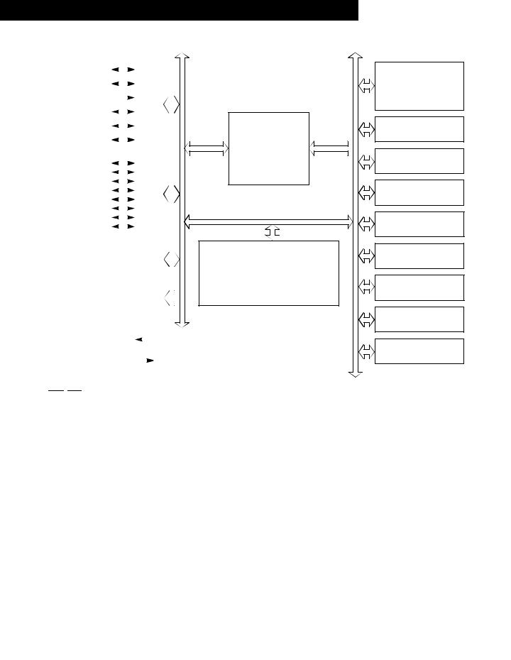
Figure 1-1 shows the structure of the MC68HC908QY4.
1.4 Pin Assignments
The MC68HC908QT4, MC68HC908QT2, and MC68HC908QT1 are available in 8-pin packages and the MC68HC908QY4, MC68HC908QY2, and MC68HC908QY1 in 16-pin packages. Figure 1-2 shows the pin assignment for these packages.
MC68HC908QY/QT Family — Rev. 3 |
Data Sheet |
|
|
MOTOROLA |
General Description |
19 |
General Description
PTA0/AD0/TCH0/KBI0 |
|
|
|
|
|
|
|
|
|
|
|
|||||
|
|
|
|
|
|
|
|
|
|
|
||||||
PTA1/AD1/TCH1/KBI1 |
|
|
|
|
|
|
|
|
|
|
|
|||||
|
|
|
|
|
|
|
|
|
|
|
||||||
|
|
|
|
|
|
|
|
|
|
|
|
|
|
|
|
|
PTA2/IRQ/KBI2/TCLK |
|
|
|
|
PTA |
|
DDRA |
|
|
|||||||
|
|
|
|
|
|
|
||||||||||
|
|
|
|
|
|
|
|
|
|
|
|
|
||||
|
PTA3/RST/KBI3 |
|
|
|
|
|
|
|
||||||||
|
|
|
|
|
|
|
|
|
|
|
|
|||||
PTA4/OSC2/AD2/KBI4 |
|
|
|
|
|
|
|
|
|
|
|
|||||
|
|
|
|
|
|
|
|
|
|
|
||||||
PTA5/OSC1/AD3/KBI5 |
|
|
|
|
|
|
|
|
|
|
|
|||||
|
|
|
|
|
|
|
|
|
|
|
||||||
|
|
|
PTB0 |
|
|
|
|
|
|
|
|
|
|
|
||
|
|
|
|
|
|
|
|
|
|
|
|
|
|
|||
|
|
|
|
|
|
|
|
|
|
|
|
|
|
|||
|
|
|
|
|
|
|
|
|
|
|
|
|
|
|||
|
|
|
PTB1 |
|
|
|
|
|
|
|
|
|
|
|
||
|
|
|
|
|
|
|
|
|
|
|
|
|
|
|||
|
|
|
PTB2 |
|
|
|
|
PTB |
|
DDRB |
|
|
||||
|
|
|
|
|
|
|
|
|
|
|||||||
|
|
|
PTB4 |
|
|
|
|
|
|
|
||||||
|
|
|
PTB3 |
|
|
|
|
|
|
|
|
|
|
|
||
|
|
|
|
|
|
|
|
|
|
|
|
|
|
|||
|
|
|
PTB5 |
|
|
|
|
|
|
|
|
|
|
|
||
|
|
|
|
|
|
|
|
|
|
|
|
|
|
|||
|
|
|
|
|
|
|
|
|
|
|
|
|
|
|||
|
|
|
PTB6 |
|
|
|
|
|
|
|
|
|
|
|
||
|
|
|
|
|
|
|
|
|
|
|
|
|
|
|||
|
|
|
PTB7 |
|
|
|
|
|
|
|
|
|
|
|
||
|
|
|
|
|
|
|
|
|
|
|
|
|
|
|||
|
|
|
|
|
|
|
|
|
|
|
|
|
|
|
|
|
|
|
|
|
|
|
|
|
|
|
|
|
|
|
|
||
|
|
|
|
|
|
|
|
8-BIT ADC |
|
|
|
|||||
|
|
|
|
|
|
|
|
|
|
|
||||||
|
|
|
|
|
|
|
|
|
|
|
||||||
|
|
|
|
|
|
|
|
|
|
|
|
|
|
|
|
|
|
|
|
|
|
|
|
|
|
|
|
|
|||||
|
|
|
|
|
|
128 BYTES RAM |
|
|
||||||||
|
|
|
|
|
|
|
|
|||||||||
|
|
|
|
|
|
|
|
|||||||||
|
|
|
|
|
|
|
|
|
|
|
|
|
|
|
|
|
|
|
|
|
|
|
|
|
|
|
|
|
|
|
VDD |
|
|
|
POWER SUPPLY |
|
|
|
|
|
||||||||||
|
|
|
|
|
|
|||||||||||
|
|
|
|
|
||||||||||||
|
|
|
|
|
|
|
|
|
|
|
|
|
|
VSS |
|
|
|
|
|
|
|
|
|
|
|
|
|
|
|
|
|
||
M68HC08 CPU
MC68HC908QY4 AND MC68HC908QT4
4096 BYTES
MC68HC908QY2, MC68HC908QY1, MC68HC908QT2, AND MC68HC908QT1: 1536 BYTES
USER FLASH
CLOCK
GENERATOR (OSCILLATOR)
SYSTEM INTEGRATION
MODULE
SINGLE INTERRUPT
MODULE
BREAK
MODULE
POWER-ON RESET
MODULE
KEYBOARD INTERRUPT
MODULE
16-BIT TIMER
MODULE
COP
MODULE
MONITOR ROM
RST, IRQ: Pins have internal (about 30K Ohms) pull up
PTA[0:5]: High current sink and source capability
PTA[0:5]: Pins have programmable keyboard interrupt and pull up
PTB[0:7]: Not available on 8-pin devices – MC68HC908QT1, MC68HC908QT2, and MC68HC908QT4
ADC: Not available on the MC68HC908QY1 and MC68HC908QT1
Figure 1-1. Block Diagram
Data Sheet |
MC68HC908QY/QT Family — Rev. 3 |
|
|
20 |
General Description |
MOTOROLA |
General Description
Pin Assignments
VDD |
1 |
8 |
VSS |
PTA5/OSC1/KBI5 |
2 |
7 |
PTA0/TCH0/KBI0 |
PTA4/OSC2/KBI4 |
3 |
6 |
PTA1/TCH1/KBI1 |
PTA3/RST/KBI3 |
4 |
5 |
PTA2/IRQ/KBI2/TCLK |
|
|
VDD |
|
|
1 |
8 |
|
VSS |
|||
|
|
|
|||||||||
PTA5/OSC1/AD3/KBI5 |
|
|
|
2 |
7 |
|
PTA0/AD0/TCH0/KBI0 |
||||
|
|
|
|
||||||||
PTA4/OSC2/AD2/KBI4 |
|
|
3 |
6 |
|
PTA1/AD1/TCH1/KBI1 |
|||||
|
|
|
|||||||||
|
|
|
|
|
|
|
|
|
|
|
|
PTA3/RST/KBI3 |
|
|
4 |
5 |
|
PTA2/IRQ/KBI2/TCLK |
|||||
|
|
|
|
|
|
|
|
|
|
|
|
8-PIN ASSIGNMENT |
8-PIN ASSIGNMENT |
MC68HC908QT1 PDIP/SOIC |
MC68HC908QT2 AND MC68HC908QT4 PDIP/SOIC |
VDD |
1 |
16 |
PTB7 |
2 |
15 |
PTB6 |
3 |
14 |
PTA5/OSC1/KBI5 |
4 |
13 |
PTA4/OSC2/KBI4 |
5 |
12 |
PTB5 |
6 |
11 |
PTB4 |
7 |
10 |
PTA3/RST/KBI3 |
8 |
9 |
VSS |
|
|
VDD |
|
|
1 |
16 |
|
VSS |
||||
|
|
|
|||||||||||
|
|
|
|||||||||||
PTB0 |
|
PTB7 |
|
|
2 |
15 |
|
PTB0 |
|||||
PTB1 |
|
PTB6 |
|
|
3 |
14 |
|
PTB1 |
|||||
|
|
|
|||||||||||
PTA0/TCH0/KBI0 |
PTA5/OSC1/AD3/KBI5 |
|
|
4 |
13 |
|
PTA0/AD0/TCH0/KBI0 |
||||||
|
|
|
|||||||||||
PTA1/TCH1/KBI1 |
PTA4/OSC2/AD2/KBI4 |
|
|
5 |
12 |
|
PTA1/AD1/TCH1/KBI1 |
||||||
|
|
|
|||||||||||
PTB2 |
|
PTB5 |
|
|
6 |
11 |
|
PTB2 |
|||||
|
|
|
|||||||||||
PTB3 |
|
PTB4 |
|
|
7 |
10 |
|
PTB3 |
|||||
|
|
|
|||||||||||
|
|
|
|
|
|
|
|
|
|
|
|
|
|
PTA2/IRQ/KBI2/TCLK |
PTA3/RST/KBI3 |
|
|
8 |
9 |
|
PTA2/IRQ/KBI2/TCLK |
||||||
|
|
|
|
|
|
|
|
|
|
|
|
|
|
16-PIN ASSIGNMENT |
16-PIN ASSIGNMENT |
MC68HC908QY1 PDIP/SOIC |
MC68HC908QY2 AND MC68HC908QY4 PDIP/SOIC |
PTA0/TCH0/KBI0 |
|
|
1 |
16 |
|
PTA1/TCH1/KBI1 |
PTA0/AD0/TCH0/KBI0 |
|
1 |
16 |
|
PTA1/AD1/TCH1/KBI1 |
||||
|
|
|
|
|
||||||||||||
|
|
|
|
|
||||||||||||
PTB1 |
|
|
2 |
15 |
|
PTB2 |
PTB1 |
|
2 |
15 |
|
PTB2 |
||||
|
|
|
|
|
||||||||||||
PTB0 |
|
|
3 |
14 |
|
PTB3 |
PTB0 |
|
3 |
14 |
|
PTB3 |
||||
|
|
|
|
|
||||||||||||
VSS |
|
|
4 |
13 |
|
PTA2/ |
|
/KBI2/TCLK |
VSS |
|
4 |
13 |
|
PTA2/ |
|
/KBI2/TCLK |
|
|
|
IRQ |
IRQ |
||||||||||||
|
|
|
|
|
||||||||||||
|
|
|
|
|||||||||||||
VDD |
|
|
5 |
12 |
|
PTA3/RST/KBI3 |
VDD |
|
5 |
12 |
|
PTA3/RST/KBI3 |
||||
|
|
|
|
|
||||||||||||
|
|
|
|
|||||||||||||
PTB7 |
|
|
6 |
11 |
|
PTB4 |
PTB7 |
|
6 |
11 |
|
PTB4 |
||||
|
|
|
|
|
||||||||||||
|
|
|
|
|||||||||||||
PTB6 |
|
|
7 |
10 |
|
PTB5 |
PTB6 |
|
7 |
10 |
|
PTB5 |
||||
|
|
|
|
|
||||||||||||
|
|
|
|
|||||||||||||
PTA5/OSC1/KBI5 |
|
|
8 |
9 |
|
PTA4/OSC2/KBI4 |
PTA5/OSC1/AD3/KBI5 |
|
8 |
9 |
|
PTA4/OSC2/AD2/KBI4 |
||||
|
|
|
|
|
||||||||||||
|
|
|
|
|||||||||||||
|
|
|
16-PIN ASSIGNMENT |
|
|
|
|
|
16-PIN ASSIGNMENT |
|
|
|
||||
|
|
|
MC68HC908QY1 TSSOP |
|
|
|
MC68HC908QY2 AND MC68HC908QY4 TSSOP |
|||||||||
PTA0/TCH0/KBI0 |
1 |
|
|
|
|
|
|
|
|
|
|
|
|
|
|
8 |
PTA1/TCH1/KBI1 |
PTA0/AD0/TCH0/KBI0 |
1 |
|
|
|
|
|
|
|
|
|
|
|
|
|
|
8 |
PTA1/AD1/TCH1/KBI1 |
||||||
|
|
|
|
|
|
|
|
|
|
|
|
|
|
|
|
|
|
|
|
|
|
|
|
|
|
|
|
||||||||||||||
|
|
|
|||||||||||||||||||||||||||||||||||||||
|
|
||||||||||||||||||||||||||||||||||||||||
VSS |
2 |
|
|
|
|
|
|
|
|
|
|
|
|
|
7 |
|
|
|
|
VSS |
2 |
|
|
|
|
|
|
|
|
|
|
|
|
|
|
7 |
|
|
|
|
|
|
|
|
|
|
|
|
|
|
|
|
|
|
|
|
|
|
|
|
|
|
|
|
|
|
|
|
|
|
|
|
|
|
|
|
|
||||||
|
|
|
|
|
|
|
|
|
|
|
|
|
|
PTA2/IRQ/KBI2/TCLK |
|
|
|
|
|
|
|
|
|
|
|
|
|
|
PTA2/IRQ/KBI2/TCLK |
||||||||||||
|
|
||||||||||||||||||||||||||||||||||||||||
|
|
|
|
|
|
|
|
|
|
|
|
|
|
|
|||||||||||||||||||||||||||
VDD |
3 |
|
|
|
|
|
|
|
|
|
|
|
|
|
|
6 |
|
|
|
|
|
|
|
|
|
|
|
|
|
|
|
|
|
|
|
|
|
|
|
|
|
|
|
|
|
|
|
|
|
|
|
|
|
|
|
PTA3/RST/KBI3 |
VDD |
3 |
|
|
|
|
|
|
|
|
|
|
|
|
|
|
6 |
PTA3/RST/KBI3 |
|||||||||
PTA5/OSC1/KB15 |
4 |
|
|
|
|
|
|
|
|
|
|
|
|
|
|
5 |
PTA4/OSC2/KBI4 |
PTA5//OSC1/AD3/KB15 |
4 |
|
|
|
|
|
|
|
|
|
|
|
|
|
|
5 |
PTA4/OSC2/AD2/KBI4 |
||||||
|
|
|
|
||||||||||||||||||||||||||||||||||||||
|
|
|
|
|
|
|
|
|
|
|
|
|
|
|
|
|
|
|
|
|
|
|
|
|
|
|
|
|
|
|
|
|
|
|
|
|
|
|
|
|
|
|
8-PIN ASSIGNMENT |
|
|
|
|
|
8-PIN ASSIGNMENT |
|
|
|
|
||||||||||||||||||||||||||||||
|
MC68HC908QT1 DFN |
|
|
|
|
MC68HC908QT2 AND MC68HC908QT4 DFN |
|||||||||||||||||||||||||||||||||||
Figure 1-2. MCU Pin Assignments
MC68HC908QY/QT Family — Rev. 3 |
Data Sheet |
|
|
MOTOROLA |
General Description |
21 |

General Description
1.5 Pin Functions
Table 1-2 provides a description of the pin functions.
Table 1-2. Pin Functions
Pin |
|
|
|
Description |
Input/Output |
Name |
|
|
|
||
|
|
|
|
|
|
|
|
|
|
||
VDD |
|
Power supply |
Power |
||
VSS |
|
Power supply ground |
Power |
||
|
|
PTA0 — General purpose I/O port |
Input/Output |
||
|
|
|
|
||
PTA0 |
|
AD0 — A/D channel 0 input |
Input |
||
|
|
|
|
|
|
|
TCH0 — Timer Channel 0 I/O |
Input/Output |
|||
|
|
||||
|
|
|
|
||
|
|
KBI0 — Keyboard interrupt input 0 |
Input |
||
|
|
|
|
||
|
|
PTA1 — General purpose I/O port |
Input/Output |
||
|
|
|
|
||
PTA1 |
|
AD1 — A/D channel 1 input |
Input |
||
|
|
|
|
|
|
|
TCH1 — Timer Channel 1 I/O |
Input/Output |
|||
|
|
||||
|
|
|
|
||
|
|
KBI1 — Keyboard interrupt input 1 |
Input |
||
|
|
|
|
||
|
|
PTA2 — General purpose input-only port |
Input |
||
|
|
|
|
|
|
|
|
|
|
— External interrupt with programmable pullup and Schmitt trigger input |
Input |
PTA2 |
|
IRQ |
|||
|
|
|
|
|
|
|
KBI2 — Keyboard interrupt input 2 |
Input |
|||
|
|
||||
|
|
|
|
||
|
|
TCLK — Timer clock input |
Input |
||
|
|
|
|
||
|
|
PTA3 — General purpose I/O port |
Input/Output |
||
|
|
|
|
|
|
PTA3 |
|
|
|
— Reset input, active low with internal pullup and Schmitt trigger |
Input |
RST |
|||||
|
|
|
|
||
|
|
KBI3 — Keyboard interrupt input 3 |
Input |
||
|
|
|
|
||
|
|
PTA4 — General purpose I/O port |
Input/Output |
||
|
|
|
|
||
|
|
OSC2 — XTAL oscillator ou tput (XTAL option only) |
Output |
||
PTA4 |
|
|
|
RC or internal oscillator output (OSC2EN = 1 in PTAPUE register) |
Output |
|
|
|
|
|
|
|
|
AD2 — A/D channel 2 input |
Input |
||
|
|
|
|
||
|
|
KBI4 — Keyboard interrupt input 4 |
Input |
||
|
|
|
|
||
|
|
PTA5 — General purpose I/O port |
Input/Output |
||
|
|
|
|
||
PTA5 |
|
OSC1 — XTAL, RC, or external oscillator input |
Input |
||
|
|
|
|
|
|
|
AD3 — A/D channel 3 input |
Input |
|||
|
|
||||
|
|
|
|
||
|
|
KBI5 — Keyboard interrupt input 5 |
Input |
||
|
|
|
|
||
PTB[0:7](1) |
|
8 general-purpose I/O ports |
Input/Output |
||
1. The PTB pins are not available on the 8-pin packages.
Data Sheet |
|
MC68HC908QY/QT Family — Rev. 3 |
|
|
|
22 |
General Description |
MOTOROLA |

General Description
Pin Function Priority
1.6 Pin Function Priority
Table 1-3 is meant to resolve the priority if multiple functions are enabled on a single pin.
NOTE: Upon reset all pins come up as input ports regardless of the priority table.
|
Table 1-3. Function Priority in Shared Pins |
||||
|
|
|
|
|
|
Pin Name |
|
|
|
|
Highest-to-Lowest Priority Sequence |
|
|
|
|
||
PTA0 |
|
|
AD0 → TCH0 → KBI0 → PTA0 |
||
|
|
|
|
||
PTA1 |
|
|
AD1 →TCH1 → KBI1 → PTA1 |
||
|
|
|
|
|
|
PTA2 |
|
|
|
|
→ KBI2 → TCLK → PTA2 |
|
|
IRQ |
|||
|
|
|
|
|
|
PTA3 |
|
|
|
|
→ KBI3 → PTA3 |
|
|
RST |
|||
|
|
|
|
||
PTA4 |
|
|
OSC2 → AD2 → KBI4 → PTA4 |
||
|
|
|
|
||
PTA5 |
|
|
OSC1 → AD3 → KBI5 → PTA5 |
||
|
|
|
|
|
|
MC68HC908QY/QT Family — Rev. 3 |
Data Sheet |
|
|
MOTOROLA |
General Description |
23 |

General Description
Data Sheet |
MC68HC908QY/QT Family — Rev. 3 |
|
|
24 |
General Description |
MOTOROLA |

Data Sheet — MC68HC908QY/QT Family
Section 2. Memory
2.1 Introduction
The central processor unit (CPU08) can address 64 Kbytes of memory space. The memory map, shown in Figure 2-1, includes:
•4096 bytes of user FLASH for MC68HC908QT4 and MC68HC908QY4
•1536 bytes of user FLASH for MC68HC908QT2, MC68HC908QT1, MC68HC908QY2, and MC68HC908QY1
•128 bytes of random access memory (RAM)
•48 bytes of user-defined vectors, located in FLASH
•416 bytes of monitor read-only memory (ROM)
•1536 bytes of FLASH program and erase routines, located in ROM
2.2Unimplemented Memory Locations
Accessing an unimplemented location can have unpredictable effects on MCU operation. In Figure 2-1 and in register figures in this document, unimplemented locations are shaded.
2.3 Reserved Memory Locations
Accessing a reserved location can have unpredictable effects on MCU operation. In Figure 2-1 and in register figures in this document, reserved locations are marked with the word Reserved or with the letter R.
MC68HC908QY/QT Family — Rev. 3 |
Data Sheet |
|
|
MOTOROLA |
Memory |
25 |

Memory
$0000
↓
$003F
$0040
↓
$007F
$0080
↓
$00FF
$0100
↓
$27FF
$2800
↓
$2DFF
$2E00
↓
$EDFF
$EE00
↓
$FDFF
$FE00
$FE01
$FE02
$FE03
$FE04
$FE05
$FE06
$FE07
$FE08
$FE09
$FE0A
$FE0B
$FE0C
$FE0D
↓
$FE0F
$FE10
↓
$FFAF
$FFB0
↓
$FFBD
$FFBE
$FFBF
$FFC0
$FFC1
$FFC2
↓
$FFCF
$FFD0
↓
$FFFF
I/O REGISTERS
64 BYTES
RESERVED(1)
64 BYTES
RAM
128 BYTES
UNIMPLEMENTED(1)
9984 BYTES
AUXILIARY ROM
1536 BYTES
UNIMPLEMENTED(1)
49152 BYTES
FLASH MEMORY
MC68HC908QT4 AND MC68HC908QY4
4096 BYTES
BREAK STATUS REGISTER (BSR)
RESET STATUS REGISTER (SRSR)
BREAK AUXILIARY REGISTER (BRKAR)
BREAK FLAG CONTROL REGISTER (BFCR)
INTERRUPT STATUS REGISTER 1 (INT1)
INTERRUPT STATUS REGISTER 2 (INT2)
INTERRUPT STATUS REGISTER 3 (INT3)
RESERVED FOR FLASH TEST CONTROL REGISTER (FLTCR)
FLASH CONTROL REGISTER (FLCR)
BREAK ADDRESS HIGH REGISTER (BRKH)
BREAK ADDRESS LOW REGISTER (BRKL)
BREAK STATUS AND CONTROL REGISTER (BRKSCR)
LVISR
RESERVED FOR FLASH TEST
3 BYTES
MONITOR ROM 416 BYTES
FLASH
14 BYTES
FLASH BLOCK PROTECT REGISTER (FLBPR)
RESERVED FLASH
INTERNAL OSCILLATOR TRIM VALUE
RESERVED FLASH
FLASH
14 BYTES
USER VECTORS
48 BYTES
Note 1.
Attempts to execute code from addresses in this range will generate an illegal address reset.
|
$2E00 |
|
UNIMPLEMENTED |
↓ |
|
51712 BYTES |
||
|
||
|
$F7FF |
|
FLASH MEMORY |
$F800 |
|
↓ |
||
1536 BYTES |
||
$FDFF |
||
|
||
|
|
MC68HC908QT1, MC68HC908QT2,
MC68HC908QY1, and MC68HC908QY2
Memory Map
Figure 2-1. Memory Map
Data Sheet |
MC68HC908QY/QT Family — Rev. 3 |
|
|
26 |
Memory |
MOTOROLA |

Memory
Input/Output (I/O) Section
2.4 Input/Output (I/O) Section
Addresses $0000–$003F, shown in Figure 2-2, contain most of the control, status, and data registers. Additional I/O registers have these addresses:
•$FE00 — Break status register, BSR
•$FE01 — Reset status register, SRSR
•$FE02 — Break auxiliary register, BRKAR
•$FE03 — Break flag control register, BFCR
•$FE04 — Interrupt status register 1, INT1
•$FE05 — Interrupt status register 2, INT2
•$FE06 — Interrupt status register 3, INT3
•$FE07 — Reserved
•$FE08 — FLASH control register, FLCR
•$FE09 — Break address register high, BRKH
•$FE0A — Break address register low, BRKL
•$FE0B — Break status and control register, BRKSCR
•$FE0C — LVI status register, LVISR
•$FE0D — Reserved
•$FFBE — FLASH block protect register, FLBPR
•$FFC0 — Internal OSC trim value — Optional
•$FFFF — COP control register, COPCTL
MC68HC908QY/QT Family — Rev. 3 |
Data Sheet |
|
|
MOTOROLA |
Memory |
27 |

Memory
Addr. |
Register Name |
Bit 7 |
6 |
5 |
4 |
3 |
2 |
1 |
Bit 0 |
|
Port A Data Register |
Read: |
|
|
|
$0000 |
(PTA) |
Write: |
|
See page 106. |
Reset: |
|
|
|
|
Port B Data Register |
Read: |
|
|
|
$0001 |
(PTB) |
Write: |
|
See page 109. |
Reset: |
|
|
|
$0002 |
Unimplemented |
|
$0003 |
Unimplemented |
|
|
Data Direction Register A |
Read: |
|
|
|
$0004 |
(DDRA) |
Write: |
|
See page 107. |
Reset: |
|
|
|
|
Data Direction Register B |
Read: |
|
|
|
$0005 |
(DDRB) |
Write: |
|
See page 109. |
Reset: |
|
|
|
$0006 |
Unimplemented |
|
|
|
|
↓ |
|
|
$000A |
Unimplemented |
|
|
|
|
|
Port A Input Pullup Enable |
Read: |
|
|
|
$000B |
Register (PTAPUE) |
Write: |
|
See page 108. |
Reset: |
|
|
|
|
Port B Input Pullup Enable |
Read: |
|
|
|
$000C |
Register (PTBPUE) |
Write: |
|
See page 111. |
Reset: |
|
|
|
$000D |
|
|
↓ |
Unimplemented |
|
$0019 |
|
|
|
Keyboard Status and |
Read: |
|
|
|
$001A |
Control Register (KBSCR) |
Write: |
|
See page 88. |
Reset: |
|
|
|
|
Keyboard Interrupt |
Read: |
|
|
|
$001B |
Enable Register (KBIER) |
Write: |
|
See page 89. |
Reset: |
|
|
R |
AWUL |
PTA5 |
PTA4 |
PTA3 |
PTA2 |
PTA1 |
PTA0 |
|
|
||||||
|
|
||||||
|
|
|
|
|
|
|
|
|
|
|
Unaffected by reset |
|
|
|
|
|
|
|
|
|
|
|
|
PTB7 |
PTB6 |
PTB5 |
PTB4 |
PTB3 |
PTB2 |
PTB1 |
PTB0 |
|
|
|
|
|
|
|
|
|
|
|
Unaffected by reset |
|
|
|
|
|
|
|
|
|
|
|
|
|
|
|
|
|
|
|
|
|
|
|
|
|
|
|
|
|
|
|
|
|
|
|
|
|
|
|
|
|
|
|
|
R |
R |
DDRA5 |
DDRA4 |
DDRA3 |
0 |
DDRA1 |
DDRA0 |
|
|||||||
|
|||||||
|
|
|
|
|
|
|
|
0 |
0 |
0 |
0 |
0 |
0 |
0 |
0 |
|
|
|
|
|
|
|
|
DDRB7 |
DDRB6 |
DDRB5 |
DDRB4 |
DDRB3 |
DDRB2 |
DDRB1 |
DDRB0 |
|
|
|
|
|
|
|
|
0 |
0 |
0 |
0 |
0 |
0 |
0 |
0 |
|
|
|
|
|
|
|
|
|
|
|
|
|
|
|
|
|
|
|
|
|
|
|
|
|
|
|
|
|
|
|
|
|
|
|
|
|
|
|
|
OSC2EN |
0 |
PTAPUE5 |
PTAPUE4 |
PTAPUE3 |
PTAPUE2 |
PTAPUE1 |
PTAPUE0 |
|
|||||||
|
|||||||
|
|
|
|
|
|
|
|
0 |
0 |
0 |
0 |
0 |
0 |
0 |
0 |
|
|
|
|
|
|
|
|
PTBPUE7 |
PTBPUE6 |
PTBPUE5 |
PTBPUE4 |
PTBPUE3 |
PTBPUE2 |
PTBPUE1 |
PTBPUE0 |
|
|
|
|
|
|
|
|
0 |
0 |
0 |
0 |
0 |
0 |
0 |
0 |
|
|
|
|
|
|
|
|
|
|
|
|
|
|
|
|
|
|
|
|
|
|
|
|
0 |
0 |
0 |
0 |
KEYF |
0 |
IMASKK |
MODEK |
|
|
|
|
|
|
||
|
|
|
|
|
ACKK |
||
|
|
|
|
|
|
|
|
0 |
0 |
0 |
0 |
0 |
0 |
0 |
0 |
|
|
|
|
|
|
|
|
0 |
AWUIE |
KBIE5 |
KBIE4 |
KBIE3 |
KBIE2 |
KBIE1 |
KBIE0 |
|
|||||||
|
|||||||
|
|
|
|
|
|
|
|
0 |
0 |
0 |
0 |
0 |
0 |
0 |
0 |
|
|
|
|
|
|
|
|
|
= Unimplemented |
R |
= Reserved |
U = Unaffected |
|
||
|
|
|
|
|
|
|
|
Figure 2-2. Control, Status, and Data Registers (Sheet 1 of 5)
Data Sheet |
MC68HC908QY/QT Family — Rev. 3 |
|
|
28 |
Memory |
MOTOROLA |

Memory
Input/Output (I/O) Section
Addr. |
Register Name |
|
Bit 7 |
6 |
5 |
4 |
3 |
2 |
1 |
Bit 0 |
|
$001C |
Unimplemented |
|
|
|
|
|
|
|
|
|
|
|
|
|
|
|
|
|
|
|
|
|
|
|
IRQ Status and Control |
Read: |
0 |
0 |
0 |
0 |
IRQF |
0 |
IMASK |
MODE |
|
|
|
|
|
|
|
|
|
||||
$001D |
Register (INTSCR) |
Write: |
|
|
|
|
|
ACK |
|||
|
|
|
|
|
|
|
|||||
|
See page 81. |
Reset: |
0 |
0 |
0 |
0 |
0 |
0 |
0 |
0 |
|
|
|
||||||||||
|
|
|
|
|
|
|
|
|
|
|
|
|
Configuration Register 2 |
Read: |
IRQPUD |
IRQEN |
R |
OSCOPT1 |
OSCOPT0 |
R |
R |
RSTEN |
|
|
|
||||||||||
$001E |
(CONFIG2)(1) |
Write: |
|||||||||
|
|
|
|
|
|
|
|
||||
|
See page 56. |
|
|
|
|
|
|
|
|
|
|
|
Reset: |
0 |
0 |
0 |
0 |
0 |
0 |
0 |
0(2) |
1.One-time writable register after each reset.
2.RSTEN reset to 0 by a power-on reset (POR) only.
|
Configuration Register 1 |
Read: |
COPRS |
LVISTOP |
LVIRSTD |
LVIPWRD |
LVI5OR3 |
SSREC |
STOP |
COPD |
|
|
|
||||||||||
$001F |
(CONFIG1)(1) |
Write: |
|||||||||
|
|
|
|
|
|
|
|
||||
|
See page 56. |
|
|
|
|
|
|
|
|
|
|
|
Reset: |
0 |
0 |
0 |
0 |
0(2) |
0 |
0 |
0 |
1.One-time writable register after each reset.
2.LVI5OR3 reset to 0 by a power-on reset (POR) only.
|
TIM Status and Control |
Read: |
|
|
|
$0020 |
Register (TSC) |
Write: |
|
See page 141. |
Reset: |
|
|
|
|
TIM Counter Register High |
Read: |
|
|
|
$0021 |
(TCNTH) |
Write: |
|
See page 143. |
Reset: |
|
|
|
|
TIM Counter Register Low |
Read: |
|
|
|
$0022 |
(TCNTL) |
Write: |
|
See page 143. |
Reset: |
|
|
|
|
TIM Counter Modulo |
Read: |
|
|
|
$0023 |
Register High (TMODH) |
Write: |
|
See page 143. |
Reset: |
|
|
|
|
TIM Counter Modulo |
Read: |
|
|
|
$0024 |
Register Low (TMODL) |
Write: |
|
See page 143. |
Reset: |
|
|
|
|
TIM Channel 0 Status and |
Read: |
|
|
|
$0025 |
Control Register (TSC0) |
Write: |
|
See page 144. |
Reset: |
|
|
|
|
TIM Channel 0 |
Read: |
|
|
|
$0026 |
Register High (TCH0H) |
Write: |
|
See page 147. |
Reset: |
|
|
TOF |
TOIE |
TSTOP |
0 |
0 |
PS2 |
PS1 |
PS0 |
|
|
|
|
||||||
0 |
TRST |
|
||||||
|
|
|
|
|
|
|||
0 |
0 |
1 |
0 |
0 |
0 |
0 |
0 |
|
|
|
|
|
|
|
|
|
|
Bit 15 |
Bit 14 |
Bit 13 |
Bit 12 |
Bit 11 |
Bit 10 |
Bit 9 |
Bit 8 |
|
|
|
|
|
|
|
|
|
|
|
|
|
|
|
|
|
|
|
0 |
0 |
0 |
0 |
0 |
0 |
0 |
0 |
|
|
|
|
|
|
|
|
|
|
Bit 7 |
Bit 6 |
Bit 5 |
Bit 4 |
Bit 3 |
Bit 2 |
Bit 1 |
Bit 0 |
|
|
|
|
|
|
|
|
|
|
|
|
|
|
|
|
|
|
|
0 |
0 |
0 |
0 |
0 |
0 |
0 |
0 |
|
|
|
|
|
|
|
|
|
|
Bit 15 |
Bit 14 |
Bit 13 |
Bit 12 |
Bit 11 |
Bit 10 |
Bit 9 |
Bit 8 |
|
|
|
|
|
|
|
|
|
|
1 |
1 |
1 |
1 |
1 |
1 |
1 |
1 |
|
|
|
|
|
|
|
|
|
|
Bit 7 |
Bit 6 |
Bit 5 |
Bit 4 |
Bit 3 |
Bit 2 |
Bit 1 |
Bit 0 |
|
|
|
|
|
|
|
|
|
|
1 |
1 |
1 |
1 |
1 |
1 |
1 |
1 |
|
|
|
|
|
|
|
|
|
|
CH0F |
CH0IE |
MS0B |
MS0A |
ELS0B |
ELS0A |
TOV0 |
CH0MAX |
|
|
||||||||
0 |
||||||||
|
|
|
|
|
|
|
||
|
|
|
|
|
|
|
|
|
0 |
0 |
0 |
0 |
0 |
0 |
0 |
0 |
|
|
|
|
|
|
|
|
|
|
Bit 15 |
Bit 14 |
Bit 13 |
Bit 12 |
Bit 11 |
Bit 10 |
Bit 9 |
Bit 8 |
|
|
|
|
|
|
|
|
|
|
|
|
|
Indeterminate after reset |
|
|
|
||
|
|
|
|
|
|
|
|
|
|
= Unimplemented |
R |
= Reserved |
U = Unaffected |
|
|||
|
|
|
|
|
|
|
|
|
Figure 2-2. Control, Status, and Data Registers (Sheet 2 of 5)
MC68HC908QY/QT Family — Rev. 3 |
Data Sheet |
|
|
MOTOROLA |
Memory |
29 |

Memory
Addr. |
Register Name |
|
Bit 7 |
6 |
5 |
4 |
3 |
2 |
1 |
Bit 0 |
|
|
TIM Channel 0 |
Read: |
Bit 7 |
Bit 6 |
Bit 5 |
Bit 4 |
Bit 3 |
Bit 2 |
Bit 1 |
Bit 0 |
|
|
|
||||||||||
$0027 |
Register Low (TCH0L) |
Write: |
|||||||||
|
|
|
|
|
|
|
|
||||
|
See page 147. |
|
|
|
|
|
|
|
|
|
|
|
Reset: |
|
|
|
Indeterminate after reset |
|
|
|
|||
|
|
|
|
|
|
|
|
||||
|
|
|
|
|
|
|
|
|
|
|
|
|
TIM Channel 1 Status and |
Read: |
CH1F |
CH1IE |
0 |
MS1A |
ELS1B |
ELS1A |
TOV1 |
CH1MAX |
|
|
|
|
|
||||||||
$0028 |
Control Register (TSC1) |
Write: |
0 |
|
|||||||
|
|
|
|
|
|
|
|||||
|
See page 144. |
Reset: |
0 |
0 |
0 |
0 |
0 |
0 |
0 |
0 |
|
|
|
||||||||||
|
|
|
|
|
|
|
|
|
|
|
|
|
TIM Channel 1 |
Read: |
Bit 15 |
Bit 14 |
Bit 13 |
Bit 12 |
Bit 11 |
Bit 10 |
Bit 9 |
Bit 8 |
|
|
|
||||||||||
$0029 |
Register High (TCH1H) |
Write: |
|||||||||
|
|
|
|
|
|
|
|
||||
|
See page 147. |
|
|
|
|
|
|
|
|
|
|
|
Reset: |
|
|
|
Indeterminate after reset |
|
|
|
|||
|
|
|
|
|
|
|
|
||||
|
|
|
|
|
|
|
|
|
|
|
|
|
TIM Channel 1 |
Read: |
Bit 7 |
Bit 6 |
Bit 5 |
Bit 4 |
Bit 3 |
Bit 2 |
Bit 1 |
Bit 0 |
|
|
|
||||||||||
$002A |
Register Low (TCH1L) |
Write: |
|||||||||
|
|
|
|
|
|
|
|
||||
|
See page 147. |
|
|
|
|
|
|
|
|
|
|
|
Reset: |
|
|
|
Indeterminate after reset |
|
|
|
|||
|
|
|
|
|
|
|
|
||||
$002B |
|
|
|
|
|
|
|
|
|
|
|
|
|
|
|
|
|
|
|
|
|
||
↓ |
Unimplemented |
|
|
|
|
|
|
|
|
|
|
$0035 |
|
|
|
|
|
|
|
|
|
|
|
|
|
|
|
|
|
|
|
|
|
|
|
|
Oscillator Status Register |
Read: |
R |
R |
R |
R |
R |
R |
ECGON |
ECGST |
|
|
|
|
|||||||||
$0036 |
(OSCSTAT) |
Write: |
|
||||||||
|
|
|
|
|
|
|
|
||||
|
See page 103. |
Reset: |
0 |
0 |
0 |
0 |
0 |
0 |
0 |
0 |
|
|
|
||||||||||
$0037 |
Unimplemented |
Read: |
|
|
|
|
|
|
|
|
|
|
|
|
|
|
|
|
|
||||
|
|
|
|
|
|
|
|
|
|
|
|
|
Oscillator Trim Register |
Read: |
TRIM7 |
TRIM6 |
TRIM5 |
TRIM4 |
TRIM3 |
TRIM2 |
TRIM1 |
TRIM0 |
|
$0038 |
(OSCTRIM) |
Write: |
|||||||||
|
|
|
|
|
|
|
|
||||
See page 104. |
|
|
|
|
|
|
|
|
|||
|
|
|
|
|
|
|
|
|
|
||
|
Reset: |
1 |
0 |
0 |
0 |
0 |
0 |
0 |
0 |
||
|
|
||||||||||
$0039 |
|
|
|
|
|
|
|
|
|
|
|
|
|
|
|
|
|
|
|
|
|
||
↓ |
Unimplemented |
|
|
|
|
|
|
|
|
|
|
$003B |
|
|
|
|
|
|
|
|
|
|
|
|
|
|
|
|
|
|
|
|
|
|
|
|
ADC Status and Control |
Read: |
COCO |
AIEN |
ADCO |
CH4 |
CH3 |
CH2 |
CH1 |
CH0 |
|
|
|
|
|||||||||
$003C |
Register (ADSCR) |
Write: |
|
||||||||
|
|
|
|
|
|
|
|
||||
|
See page 46. |
Reset: |
0 |
0 |
0 |
1 |
1 |
1 |
1 |
1 |
|
|
|
||||||||||
$003D |
Unimplemented |
|
|
|
|
|
|
|
|
|
|
|
|
|
|
|
|
|
|
|
|||
|
|
|
|
|
|
|
|
|
|
|
|
|
ADC Data Register |
Read: |
Bit 7 |
Bit 6 |
Bit 5 |
Bit 4 |
Bit 3 |
Bit 2 |
Bit 1 |
Bit 0 |
|
|
|
||||||||||
$003E |
(ADR) |
Write: |
|||||||||
|
|
|
|
|
|
|
|
||||
|
See page 47. |
|
|
|
|
|
|
|
|
|
|
|
Reset: |
|
|
|
Indeterminate after reset |
|
|
|
|||
|
|
|
|
|
|
|
|
||||
|
|
|
|
|
|
|
|
|
|
|
|
|
|
|
|
= Unimplemented |
R |
= Reserved |
U = Unaffected |
|
|||
|
|
|
|
|
|
|
|
|
|
|
|
Figure 2-2. Control, Status, and Data Registers (Sheet 3 of 5)
Data Sheet |
|
MC68HC908QY/QT Family — Rev. 3 |
|
|
|
30 |
Memory |
MOTOROLA |
Loading...