


 Loading...
Motorola MC68HC711P2CFS4, MC68HC711P2CFN3, MC68HC711P2CFN4, MC68HC11P0CFN3, MC68HC11P1CFN3 Datasheet
...MC68HC11P2
MC68HC711P2
Technical Data
M68HC11
Microcontrollers
MC68HC11P2/D
Rev. 1, 4/2002
WWW.MOTOROLA.COM/SEMICONDUCTORS

MC68HC11P2
MC68HC711P2
Technical Data — Rev 1.0
Motorola reserves the right to make changes without further notice to any products herein. Motorola makes no warranty, representation or guarantee regarding the suitability of its products for any particular purpose, nor does Motorola assume any liability arising out of the application or use of any product or circuit, and specifically disclaims any and all liability, including without limitation consequential or incidental damages. "Typical" parameters which may be provided in Motorola data sheets and/or specifications can and do vary in different applications and actual performance may vary over time. All operating parameters, including "Typicals" must be validated for each customer application by customer’s technical experts. Motorola does not convey any license under its patent rights nor the rights of others. Motorola products are not designed, intended, or authorized for use as components in systems intended for surgical implant into the body, or other applications intended to support or sustain life, or for any other application in which the failure of the Motorola product could create a situation where personal injury or death may occur. Should Buyer purchase or use Motorola products for any such unintended or unauthorized application, Buyer shall indemnify and hold Motorola and its officers, employees, subsidiaries, affiliates, and distributors harmless against all claims, costs, damages, and expenses, and reasonable attorney fees arising out of, directly or indirectly, any claim of personal injury or death associated with such unintended or unauthorized use, even if such claim alleges that Motorola was negligent regarding the design or manufacture of the part. Motorola, Inc. is an Equal Opportunity/Affirmative Action Employer.
Motorola and |
are registered trademarks of Motorola, Inc. |
|
DigitalDNA is a trademark of Motorola, Inc. |
© Motorola, Inc., 2002 |
|
MC68HC11P2 — Rev 1.0 |
Technical Data |
|
|
|
|
|
|
|
MOTOROLA |
|
3 |
|
|
|
|
|
Technical Data |
MC68HC11P2 — Rev 1.0 |
|
|
|
|
|
|
|
|
|
4 |
MOTOROLA |
||

Technical Data — MC68HC11P2
List of Paragraphs
List of Paragraphs. . . . . . . . . . . . . . . . . . . . . . . . . . . . . . . . 5
Table of Contents . . . . . . . . . . . . . . . . . . . . . . . . . . . . . . . . 7
List of Figures . . . . . . . . . . . . . . . . . . . . . . . . . . . . . . . . . . 13
List of Tables . . . . . . . . . . . . . . . . . . . . . . . . . . . . . . . . . . . 15
Section 1. General Description . . . . . . . . . . . . . . . . . . . . 17
Section 2. Pin Descriptions . . . . . . . . . . . . . . . . . . . . . . . 21
Section 3. Operating Modes and On-Chip Memory . . . . 41
Section 4. Parallel Input/Output . . . . . . . . . . . . . . . . . . . . 73
Section 5. Serial Communications Interface (SCI) . . . . . 87
Section 6. Motorola Interconnect Bus (MI BUS). . . . . . 109
Section 7. Serial Peripheral Interface (SPI). . . . . . . . . . 125
Section 8. Timing System. . . . . . . . . . . . . . . . . . . . . . . . 137
Section 9. Analog-to-Digital Converter . . . . . . . . . . . . . 173
Section 10. Resets and Interrupts . . . . . . . . . . . . . . . . . 185
Section 11. CPU Core and Instruction Set . . . . . . . . . . 213
Section 12. Electrical Specifications . . . . . . . . . . . . . . . 231
Section 13. Mechanical Data . . . . . . . . . . . . . . . . . . . . . 247
Section 14. Ordering Information . . . . . . . . . . . . . . . . . 251
Section 15. Development Support . . . . . . . . . . . . . . . . . 253
Glossary . . . . . . . . . . . . . . . . . . . . . . . . . . . . . . . . . . . . . . 255
MC68HC11P2 — |
Rev 1.0 |
Technical Data |
|
|
|
MOTOROLA |
List of Paragraphs |
5 |

List of Paragraphs
Revision History . . . . . . . . . . . . . . . . . . . . . . . . . . . . . . . 265
Technical Data |
|
MC68HC11P2 — Rev 1.0 |
|
|
|
6 |
List of Paragraphs |
MOTOROLA |

Technical Data — MC68HC11P2
Table of Contents
List of Paragraphs
Table of Contents
List of Figures
List of Tables
Section 1. General Description
1.1 Contents . . . . . . . . . . . . . . . . . . . . . . . . . . . . . . . . . . . . . . . . . .17
1.2 Introduction . . . . . . . . . . . . . . . . . . . . . . . . . . . . . . . . . . . . . . . .17
1.3 Features . . . . . . . . . . . . . . . . . . . . . . . . . . . . . . . . . . . . . . . . . .18
Section 2. Pin Descriptions
2.1 Contents . . . . . . . . . . . . . . . . . . . . . . . . . . . . . . . . . . . . . . . . . .21
2.2 Introduction . . . . . . . . . . . . . . . . . . . . . . . . . . . . . . . . . . . . . . . .21
2.3 VDD and VSS . . . . . . . . . . . . . . . . . . . . . . . . . . . . . . . . . . . . . .22
2.4 RESET . . . . . . . . . . . . . . . . . . . . . . . . . . . . . . . . . . . . . . . . . . .23
2.5 Crystal driver and external clock input (XTAL, EXTAL) . . . . . .24 2.6 E clock output (E) . . . . . . . . . . . . . . . . . . . . . . . . . . . . . . . . . . .26 2.7 Phase-locked loop (XFC, VDDSYN). . . . . . . . . . . . . . . . . . . . .26 2.8 Interrupt request (IRQ) . . . . . . . . . . . . . . . . . . . . . . . . . . . . . . .32 2.9 Nonmaskable interrupt (XIRQ/VPPE). . . . . . . . . . . . . . . . . . . .32 2.10 MODA and MODB (MODA/LIR and MODB/VSTBY) . . . . . . . .33
MC68HC11P2 — |
Rev 1.0 |
Technical Data |
|
|
|
MOTOROLA |
Table of Contents |
7 |

Table of Contents
2.11 VRH and VRL . . . . . . . . . . . . . . . . . . . . . . . . . . . . . . . . . . . . . .34 2.12 PG7/R/W. . . . . . . . . . . . . . . . . . . . . . . . . . . . . . . . . . . . . . . . . .34 2.13 Port signals . . . . . . . . . . . . . . . . . . . . . . . . . . . . . . . . . . . . . . . .34
Section 3. Operating Modes and On-Chip Memory
3.1 Contents . . . . . . . . . . . . . . . . . . . . . . . . . . . . . . . . . . . . . . . . . .41 3.2 Introduction . . . . . . . . . . . . . . . . . . . . . . . . . . . . . . . . . . . . . . . .41 3.3 Operating modes . . . . . . . . . . . . . . . . . . . . . . . . . . . . . . . . . . .41 3.4 On-chip memory . . . . . . . . . . . . . . . . . . . . . . . . . . . . . . . . . . . .44 3.5 System initialization . . . . . . . . . . . . . . . . . . . . . . . . . . . . . . . . .51
3.6 EPROM, EEPROM and CONFIG register . . . . . . . . . . . . . . . .64
Section 4. Parallel Input/Output
4.1 Contents . . . . . . . . . . . . . . . . . . . . . . . . . . . . . . . . . . . . . . . . . .73
4.2 Introduction . . . . . . . . . . . . . . . . . . . . . . . . . . . . . . . . . . . . . . . .73
4.3 Port A . . . . . . . . . . . . . . . . . . . . . . . . . . . . . . . . . . . . . . . . . . . .74
4.4 Port B . . . . . . . . . . . . . . . . . . . . . . . . . . . . . . . . . . . . . . . . . . . .75
4.5 Port C . . . . . . . . . . . . . . . . . . . . . . . . . . . . . . . . . . . . . . . . . . . .77
4.6 Port D . . . . . . . . . . . . . . . . . . . . . . . . . . . . . . . . . . . . . . . . . . . .78
4.7 Port E . . . . . . . . . . . . . . . . . . . . . . . . . . . . . . . . . . . . . . . . . . . .79
4.8 Port F . . . . . . . . . . . . . . . . . . . . . . . . . . . . . . . . . . . . . . . . . . . .80
4.9 Port G . . . . . . . . . . . . . . . . . . . . . . . . . . . . . . . . . . . . . . . . . . . .81 4.10 Port H . . . . . . . . . . . . . . . . . . . . . . . . . . . . . . . . . . . . . . . . . . . .82 4.11 Internal pull-up/pull-down resistors . . . . . . . . . . . . . . . . . . . . . .83 4.12 System configuration . . . . . . . . . . . . . . . . . . . . . . . . . . . . . . . .84
Technical Data |
|
MC68HC11P2 — Rev 1.0 |
|
|
|
8 |
Table of Contents |
MOTOROLA |
Table of Contents
Section 5. Serial Communications Interface (SCI)
5.1 Contents . . . . . . . . . . . . . . . . . . . . . . . . . . . . . . . . . . . . . . . . . .87 5.2 Introduction . . . . . . . . . . . . . . . . . . . . . . . . . . . . . . . . . . . . . . . .87 5.3 Data format . . . . . . . . . . . . . . . . . . . . . . . . . . . . . . . . . . . . . . . .88 5.4 Transmit operation . . . . . . . . . . . . . . . . . . . . . . . . . . . . . . . . . .89 5.5 Receive operation. . . . . . . . . . . . . . . . . . . . . . . . . . . . . . . . . . .89 5.6 Wakeup feature . . . . . . . . . . . . . . . . . . . . . . . . . . . . . . . . . . . .91 5.7 SCI error detection . . . . . . . . . . . . . . . . . . . . . . . . . . . . . . . . . .92 5.8 SCI registers . . . . . . . . . . . . . . . . . . . . . . . . . . . . . . . . . . . . . . .93
5.9 Status flags and interrupts . . . . . . . . . . . . . . . . . . . . . . . . . . .101 5.10 Additional SCI subsystems . . . . . . . . . . . . . . . . . . . . . . . . . . .104
Section 6. Motorola Interconnect Bus (MI BUS)
6.1 Contents . . . . . . . . . . . . . . . . . . . . . . . . . . . . . . . . . . . . . . . . .109 6.2 Introduction . . . . . . . . . . . . . . . . . . . . . . . . . . . . . . . . . . . . . . .109 6.3 Push-pull sequence . . . . . . . . . . . . . . . . . . . . . . . . . . . . . . . .111 6.4 The push field . . . . . . . . . . . . . . . . . . . . . . . . . . . . . . . . . . . . .112 6.5 The pull field . . . . . . . . . . . . . . . . . . . . . . . . . . . . . . . . . . . . . .112 6.6 Biphase coding . . . . . . . . . . . . . . . . . . . . . . . . . . . . . . . . . . . .113 6.7 Message validation . . . . . . . . . . . . . . . . . . . . . . . . . . . . . . . . .113
6.8 Interfacing to MI BUS . . . . . . . . . . . . . . . . . . . . . . . . . . . . . . .116 6.9 MI BUS clock rate . . . . . . . . . . . . . . . . . . . . . . . . . . . . . . . . . .117 6.10 SCI/MI BUS2 registers . . . . . . . . . . . . . . . . . . . . . . . . . . . . . .117 6.11 SCI/MI BUS3 registers . . . . . . . . . . . . . . . . . . . . . . . . . . . . . .123
MC68HC11P2 — |
Rev 1.0 |
Technical Data |
|
|
|
MOTOROLA |
Table of Contents |
9 |

Table of Contents |
|
|
|
|
Section 7. Serial Peripheral Interface (SPI) |
|
|
7.1 |
Contents . . . . . . . . . . . . . . . . . . . . . . . . . . . . . . . . . . . |
. . . . |
. .125 |
7.2 |
Introduction . . . . . . . . . . . . . . . . . . . . . . . . . . . . . . . . . |
. . . . |
. .125 |
7.3 |
Functional description. . . . . . . . . . . . . . . . . . . . . . . . . |
. . . . |
. .126 |
7.4 |
SPI transfer formats . . . . . . . . . . . . . . . . . . . . . . . . . . . |
. . . |
. .126 |
7.5 |
SPI signals . . . . . . . . . . . . . . . . . . . . . . . . . . . . . . . . . . |
. . . |
. .129 |
7.6 |
SPI system errors . . . . . . . . . . . . . . . . . . . . . . . . . . . . . |
. . . |
. .130 |
7.7 |
SPI registers . . . . . . . . . . . . . . . . . . . . . . . . . . . . . . . . . |
. . . |
. .132 |
|
Section 8. Timing System |
|
|
8.1 |
Contents . . . . . . . . . . . . . . . . . . . . . . . . . . . . . . . . . . . . |
. . . |
. .137 |
8.2 |
Introduction . . . . . . . . . . . . . . . . . . . . . . . . . . . . . . . . . . |
. . . |
. .137 |
8.3 |
Timer structure . . . . . . . . . . . . . . . . . . . . . . . . . . . . . . . |
. . . |
. .139 |
8.4 |
Input capture. . . . . . . . . . . . . . . . . . . . . . . . . . . . . . . . . |
. . . |
. .142 |
8.5 |
Output compare . . . . . . . . . . . . . . . . . . . . . . . . . . . . . . |
. . . |
. .145 |
8.6 |
Real-time interrupt . . . . . . . . . . . . . . . . . . . . . . . . . . . . |
. . . |
. .154 |
8.7 |
Computer operating properly watchdog function . . . . . |
. . . |
. .157 |
8.8 |
Pulse accumulator . . . . . . . . . . . . . . . . . . . . . . . . . . . . |
. . . |
. .158 |
8.9 |
Pulse-width modulation (PWM) timer . . . . . . . . . . . . . . |
. . . |
. .162 |
|
Section 9. Analog-to-Digital Converter |
|
|
9.1 |
Contents . . . . . . . . . . . . . . . . . . . . . . . . . . . . . . . . . . . . |
. . . |
. .173 |
9.2 |
Introduction . . . . . . . . . . . . . . . . . . . . . . . . . . . . . . . . . . |
. . . |
. .173 |
9.3 |
Overview. . . . . . . . . . . . . . . . . . . . . . . . . . . . . . . . . . . . |
. . . |
. .174 |
9.4 |
A/D converter power-up and clock select . . . . . . . . . . . |
. . . |
. .178 |
9.5 |
Channel assignments . . . . . . . . . . . . . . . . . . . . . . . . . . |
. . . |
. .180 |
9.6 |
Control, status and results registers . . . . . . . . . . . . . . . |
. . . |
. .181 |
Technical Data |
MC68HC11P2 — |
Rev 1.0 |
|
10 |
Table of Contents |
MOTOROLA |
|
Table of Contents
9.7 Operation in STOP and WAIT modes. . . . . . . . . . . . . . . . . . .184
Section 10. Resets and Interrupts
10.1 Contents . . . . . . . . . . . . . . . . . . . . . . . . . . . . . . . . . . . . . . . . .185 10.2 Introduction . . . . . . . . . . . . . . . . . . . . . . . . . . . . . . . . . . . . . . .185 10.3 Resets. . . . . . . . . . . . . . . . . . . . . . . . . . . . . . . . . . . . . . . . . . .185 10.4 Effects of reset . . . . . . . . . . . . . . . . . . . . . . . . . . . . . . . . . . . .192 10.5 Reset and interrupt priority . . . . . . . . . . . . . . . . . . . . . . . . . . .195 10.6 Interrupts. . . . . . . . . . . . . . . . . . . . . . . . . . . . . . . . . . . . . . . . .200 10.7 Low power operation . . . . . . . . . . . . . . . . . . . . . . . . . . . . . . .203
Section 11. CPU Core and Instruction Set
11.1 Contents . . . . . . . . . . . . . . . . . . . . . . . . . . . . . . . . . . . . . . . . .213 11.2 Introduction . . . . . . . . . . . . . . . . . . . . . . . . . . . . . . . . . . . . . . .213 11.3 Registers. . . . . . . . . . . . . . . . . . . . . . . . . . . . . . . . . . . . . . . . .214 11.4 Data types. . . . . . . . . . . . . . . . . . . . . . . . . . . . . . . . . . . . . . . .220 11.5 Opcodes and operands . . . . . . . . . . . . . . . . . . . . . . . . . . . . .220 11.6 Addressing modes . . . . . . . . . . . . . . . . . . . . . . . . . . . . . . . . .221 11.7 Instruction set . . . . . . . . . . . . . . . . . . . . . . . . . . . . . . . . . . . . .223
Section 12. Electrical Specifications
12.1 Contents . . . . . . . . . . . . . . . . . . . . . . . . . . . . . . . . . . . . . . . . .231
12.2 Introduction . . . . . . . . . . . . . . . . . . . . . . . . . . . . . . . . . . . . . . .231 12.3 Maximum ratings . . . . . . . . . . . . . . . . . . . . . . . . . . . . . . . . . .232 12.4 Thermal characteristics and power considerations. . . . . . . . .233 12.5 Test methods . . . . . . . . . . . . . . . . . . . . . . . . . . . . . . . . . . . . .234 12.6 DC electrical characteristics . . . . . . . . . . . . . . . . . . . . . . . . . .235
MC68HC11P2 — |
Rev 1.0 |
Technical Data |
|
|
|
MOTOROLA |
Table of Contents |
11 |

Table of Contents
12.7 Control timing . . . . . . . . . . . . . . . . . . . . . . . . . . . . . . . . . . . . .237
Section 13. Mechanical Data
13.1 Contents . . . . . . . . . . . . . . . . . . . . . . . . . . . . . . . . . . . . . . . . .247 13.2 Pin assignments . . . . . . . . . . . . . . . . . . . . . . . . . . . . . . . . . . .248 13.3 Package dimensions. . . . . . . . . . . . . . . . . . . . . . . . . . . . . . . .249
Section 14. Ordering Information
14.1 Contents . . . . . . . . . . . . . . . . . . . . . . . . . . . . . . . . . . . . . . . . .251
14.2 Introduction . . . . . . . . . . . . . . . . . . . . . . . . . . . . . . . . . . . . . . .251
Section 15. Development Support
15.1 Contents . . . . . . . . . . . . . . . . . . . . . . . . . . . . . . . . . . . . . . . . .253 15.2 Introduction . . . . . . . . . . . . . . . . . . . . . . . . . . . . . . . . . . . . . . .253 15.3 EVS — Evaluation system . . . . . . . . . . . . . . . . . . . . . . . . . . .253
Glossary
Revision History
15.4 Major Changes Between Revision 1.0 and Revision 0.0 . . . .265
Technical Data |
|
MC68HC11P2 — Rev 1.0 |
|
|
|
12 |
Table of Contents |
MOTOROLA |

Technical Data — MC68HC11P2
List of Figures
Figure |
Title |
Page |
1-1 MC68HC11P2/MC68HC711P2 block diagram . . . . . . . . . . . . .19 2-1 84-pin PLCC/CERQUAD pinout . . . . . . . . . . . . . . . . . . . . . . . .22 2-2 External reset circuitry . . . . . . . . . . . . . . . . . . . . . . . . . . . . . . .24 2-3 Oscillator connections. . . . . . . . . . . . . . . . . . . . . . . . . . . . . . . .25 2-4 PLL circuit . . . . . . . . . . . . . . . . . . . . . . . . . . . . . . . . . . . . . . . . .27
2-5 RAM stand-by connections. . . . . . . . . . . . . . . . . . . . . . . . . . . .33
3-1 MC68HC11P2 memory map. . . . . . . . . . . . . . . . . . . . . . . . . . .44 3-2 RAM and register overlap . . . . . . . . . . . . . . . . . . . . . . . . . . . . .57
5-1 SCI baud rate generator circuit diagram. . . . . . . . . . . . . . . . . .88
5-2 SCI1 block diagram . . . . . . . . . . . . . . . . . . . . . . . . . . . . . . . . .90 5-3 Interrupt source resolution within SCI. . . . . . . . . . . . . . . . . . .103
6-1 MI BUS timing. . . . . . . . . . . . . . . . . . . . . . . . . . . . . . . . . . . . .111
6-2 Biphase coding and error detection . . . . . . . . . . . . . . . . . . . .113 6-3 MI BUS block diagram . . . . . . . . . . . . . . . . . . . . . . . . . . . . . .115
6-4 A typical interface between the MC68HC11P2 and the MI BUS
. . . . . . . . . . . . . . . . . . . . . . . . . . . . . . . . . . . . . . . . . . . . . . . .116 7-1 SPI block diagram. . . . . . . . . . . . . . . . . . . . . . . . . . . . . . . . . .127
7-2 SPI transfer format . . . . . . . . . . . . . . . . . . . . . . . . . . . . . . . . .128
8-1 Timer clock divider chains . . . . . . . . . . . . . . . . . . . . . . . . . . .140 8-2 Capture/compare block diagram. . . . . . . . . . . . . . . . . . . . . . .141
8-3 Pulse accumulator block diagram. . . . . . . . . . . . . . . . . . . . . .159 8-4 PWM timer block diagram. . . . . . . . . . . . . . . . . . . . . . . . . . . .164 8-5 PWM duty cycle . . . . . . . . . . . . . . . . . . . . . . . . . . . . . . . . . . .170
9-1 A/D converter block diagram . . . . . . . . . . . . . . . . . . . . . . . . .174
9-2 Electrical model of an A/D input pin (in sample mode) . . . . . .175 9-3 A/D conversion sequence. . . . . . . . . . . . . . . . . . . . . . . . . . . .177
10-1 Processing flow out of reset (1 of 2) . . . . . . . . . . . . . . . . . . . .206
10-2 Processing flow out of reset (2 of 2) . . . . . . . . . . . . . . . . . . . .207 10-3 Interrupt priority resolution (1 of 3) . . . . . . . . . . . . . . . . . . . . .208
MC68HC11P2 — |
Rev 1.0 |
Technical Data |
|
|
|
MOTOROLA |
List of Figures |
13 |

List of Figures
10-4 Interrupt priority resolution (2 of 3) . . . . . . . . . . . . . . . . . . . . .209 10-5 Interrupt priority resolution (3 of 3) . . . . . . . . . . . . . . . . . . . . .210 10-6 Interrupt source resolution within the SCI subsystem. . . . . . .211 11-1 Programming model . . . . . . . . . . . . . . . . . . . . . . . . . . . . . . . .214 11-2 Stacking operations . . . . . . . . . . . . . . . . . . . . . . . . . . . . . . . .216 12-1 Test methods . . . . . . . . . . . . . . . . . . . . . . . . . . . . . . . . . . . . .234 12-2 Timer inputs . . . . . . . . . . . . . . . . . . . . . . . . . . . . . . . . . . . . . .237 12-3 Reset timing . . . . . . . . . . . . . . . . . . . . . . . . . . . . . . . . . . . . . .238 12-4 Interrupt timing . . . . . . . . . . . . . . . . . . . . . . . . . . . . . . . . . . . .238 12-5 STOP recovery timing. . . . . . . . . . . . . . . . . . . . . . . . . . . . . . .239 12-6 WAIT recovery timing . . . . . . . . . . . . . . . . . . . . . . . . . . . . . . .239 12-7 Port read timing diagram . . . . . . . . . . . . . . . . . . . . . . . . . . . .240 12-8 Port write timing diagram . . . . . . . . . . . . . . . . . . . . . . . . . . . .240
12-9 SPI master timing (CPHA = 0) . . . . . . . . . . . . . . . . . . . . . . . .243
12-10 SPI master timing (CPHA = 1) . . . . . . . . . . . . . . . . . . . . . . . .243 12-11 SPI slave timing (CPHA = 0) . . . . . . . . . . . . . . . . . . . . . . . . .244
12-12 SPI slave timing (CPHA = 1) . . . . . . . . . . . . . . . . . . . . . . . . .244
12-13 Expansion bus timing . . . . . . . . . . . . . . . . . . . . . . . . . . . . . . .246 13-1 84-pin PLCC/CERQUAD pinout . . . . . . . . . . . . . . . . . . . . . . .248
13-2 84-pin PLCC mechanical dimensions. . . . . . . . . . . . . . . . . . .249
13-3 84-pin CERQUAD mechanical dimensions . . . . . . . . . . . . . .250
Technical Data |
|
MC68HC11P2 — Rev 1.0 |
|
|
|
14 |
List of Figures |
MOTOROLA |

Technical Data — MC68HC11P2
List of Tables
Table |
Title |
Page |
2-1 Port signal functions . . . . . . . . . . . . . . . . . . . . . . . . . . . . . . . . .35 3-1 Example bootloader baud rates . . . . . . . . . . . . . . . . . . . . . . . .43 3-2 Register and control bit assignments . . . . . . . . . . . . . . . . . . . .47 3-3 Registers with limited write access . . . . . . . . . . . . . . . . . . . . . .51 3-4 Hardware mode select summary . . . . . . . . . . . . . . . . . . . . . . .53
3-5 RAM and register remapping . . . . . . . . . . . . . . . . . . . . . . . . . .56
3-6 EEPROM remapping . . . . . . . . . . . . . . . . . . . . . . . . . . . . . . . .58 3-7 EEPROM block protect. . . . . . . . . . . . . . . . . . . . . . . . . . . . . . .62
3-8 Erase mode selection . . . . . . . . . . . . . . . . . . . . . . . . . . . . . . . .67
4-1 Port configuration . . . . . . . . . . . . . . . . . . . . . . . . . . . . . . . . . . .74 5-1 Example SCI baud rate control values . . . . . . . . . . . . . . . . . . .95
7-1 SPI clock rates . . . . . . . . . . . . . . . . . . . . . . . . . . . . . . . . . . . .133
8-1 Timer resolution and capacity. . . . . . . . . . . . . . . . . . . . . . . . .139 8-2 RTI periodic rates . . . . . . . . . . . . . . . . . . . . . . . . . . . . . . . . . .154
8-3 Pulse accumulator timing . . . . . . . . . . . . . . . . . . . . . . . . . . . .158
8-4 Clock A and clock B prescalers . . . . . . . . . . . . . . . . . . . . . . .167 9-1 A/D converter channel assignments . . . . . . . . . . . . . . . . . . . .180
10-1 COP timer rate select . . . . . . . . . . . . . . . . . . . . . . . . . . . . . . .187
10-2 Reset cause, reset vector and operating mode . . . . . . . . . . .192 10-3 Highest priority interrupt selection . . . . . . . . . . . . . . . . . . . . .198
10-4 Interrupt and reset vector assignments . . . . . . . . . . . . . . . . .199 10-5 Stacking order on entry to interrupts. . . . . . . . . . . . . . . . . . . .201 11-1 Reset vector comparison . . . . . . . . . . . . . . . . . . . . . . . . . . . .217
11-2 Instruction set . . . . . . . . . . . . . . . . . . . . . . . . . . . . . . . . . . . . .223
14-1 Ordering information . . . . . . . . . . . . . . . . . . . . . . . . . . . . . . . .251 15-1 M68HC11 development tools . . . . . . . . . . . . . . . . . . . . . . . . .253
MC68HC11P2 — |
Rev 1.0 |
Technical Data |
|
|
|
MOTOROLA |
List of Tables |
15 |

List of Tables
Technical Data |
|
MC68HC11P2 — Rev 1.0 |
|
|
|
16 |
List of Tables |
MOTOROLA |

Technical Data — MC68HC11P2
Section 1. General Description
1.1 Contents
1.2 Introduction. . . . . . . . . . . . . . . . . . . . . . . . . . . . . . . . . . . . . . .17
1.3 Features. . . . . . . . . . . . . . . . . . . . . . . . . . . . . . . . . . . . . . . . . .18
1.2 Introduction
The MC68HC11P2 8-bit microcomputer is a member of the M68HC11 family of HCMOS microcomputers. In addition to 32kbytes of ROM, the MC68HC11P2 contains 1kbyte of RAM and 640 bytes of EEPROM. With its advanced timer and communication features (including MI BUS(1)) the MC68HC11P2 is especially suitable for mobile communications and automotive applications.
The MC68HC711P2 is an EPROM version of the MC68HC11P2, with the User ROM replaced by a similar amount of EPROM. All references to the MC68HC11P2 apply equally to the MC68HC711P2, unless otherwise noted. References specific to the MC68HC711P2 are italicised in the text.
1.The Motorola interconnect bus (MI BUS) is a serial communications protocol which supports distributed real-time control efficiently and with a high degree of noise immunity. It allows data to be transferred between the MCU and the slave device using only one wire, making this type of communication suitable for medium speed networks requiring very low cost multiplex wiring.
MC68HC11P2 — |
Rev 1.0 |
Technical Data |
|
|
|
MOTOROLA |
General Description |
17 |

General Description
1.3 Features
•Low power, high performance M68HC11 CPU core, with 4MHz bus capability
•Power saving PLL clock circuit, with automatic disable during WAIT mode
•32kbytes of User ROM (MC68HC11P2); 32kbytes User EPROM (MC68HC711P2)
•1kbyte of RAM
•640 bytes of byte-erasable User EEPROM, with on-chip charge pump
•Up to 50 general purpose I/O lines, plus up to 12 input-only lines
•Non-multiplexed address and data buses, permitting direct access to the full 64k address map
•16-bit timer with 3/4 input captures and 4/5 output compares; pulse accumulator and COP watchdog timer
•Three 8- or 9-bit SCI subsystems, two with MI BUS† capability
•SPI subsystem, with software selectable MSB/LSB first option
•8-channel, 8-bit analog-to-digital (A/D) converter
•Four 8-bit PWM timer channels (may be concatenated to form one, or two, 16-bit channels)
•Available in 84-pin PLCC or 84-pin CERQUAD packages
Technical Data |
|
MC68HC11P2 — Rev 1.0 |
|
|
|
18 |
General Description |
MOTOROLA |

VPPE/XIRQ  IRQ
IRQ  RESET
RESET 
 LIR/MODA

VSTBY/MODB 
XTAL  EXTAL
EXTAL  E
E XFC
XFC 
VDDSYN 
VDD
VSS
General Description
Features
|
|
|
|
|
|
|
|
|
|
|
|
|
|
|
|
|
|
|
|
|
|
Pulse accumulator |
|
|
OC1/PAI |
|
|
|
|
|
|
|
|
|
|
|
|
PA7 |
|||||||||||||||||||
|
|
|
|
|
|
|
|
|
|
|
|
|
|
|
|
|
|
|
|
|
|
|
|
|
|
|
|
|
|
|
|
|
|
|
|||||||||||||||||||||||
|
|
|
|
|
|
|
|
|
|
|
|
|
|
|
|
|
|
|
|
|
|
|
OC1/OC2 |
|
|
|
|
|
|
|
|
|
|
|
|
PA6 |
|||||||||||||||||||||
|
|
|
|
|
|
|
|
|
|
|
|
|
|
|
|
|
|
|
|
|
|
|
|
|
|
|
|
|
|
|
|
|
|
|
|
|
|
|
|
|
|
|
|
|
|
|
|||||||||||
|
|
|
|
|
|
|
|
|
|
|
|
|
|
|
|
|
|
|
|
|
|
|
|
|
|
|
|
|
|
|
|
|
|
|
|
|
|
|
|
|
|
|
|
|
|||||||||||||
|
|
|
|
|
|
|
|
|
|
|
|
|
|
|
|
|
|
|
|
|
Timer |
|
|
|
|
|
|
|
|
|
OC1/OC3 |
|
|
|
|
|
A |
|
|
|
|
PA5 |
|||||||||||||||
|
|
|
|
|
|
|
|
|
|
|
|
|
|
|
|
|
|
|
|
|
|
|
|
|
|
|
|
|
|
|
|
|
|
|
|
|
|||||||||||||||||||||
|
|
|
|
|
|
|
|
|
|
|
|
|
|
|
|
|
|
|
|
|
|
|
|
|
|
|
|
|
|
OC1/OC4 |
|
|
|
|
|
|
|
|
|
PA4 |
|||||||||||||||||
|
|
|
|
|
|
|
|
|
|
|
|
|
|
|
|
|
|
|
|
|
|
|
|
|
|
|
|
|
|
|
|
|
|
|
|
|
|
|
|
Port |
|
|
|
|
|||||||||||||
|
|
|
|
|
|
|
|
|
|
|
|
|
|
|
|
|
|
|
|
|
|
|
|
|
|
|
|
|
|
|
|
|
|
IC4/OC1/OC5 |
|
|
|
|
|
|
|
|
|
PA3 |
|||||||||||||
|
|
|
|
|
|
|
|
|
|
|
|
|
|
|
|
|
|
|
|
|
|
|
|
|
|
|
|
|
|
|
|
|
|
|
|
|
|
|
|
|
|
|
|
|
|
||||||||||||
|
|
|
|
|
|
|
|
|
|
|
|
|
|
|
|
|
|
|
|
|
|
Periodic interrupt |
|
|
|
|
|
IC1 |
|
|
|
|
|
|
|
|
|
|
|
|
PA2 |
||||||||||||||||
|
|
|
|
|
|
|
|
|
|
|
|
|
|
|
|
|
|
|
|
|
|
|
|
|
|
|
|
|
|
|
|
|
|
|
|
|
|||||||||||||||||||||
|
|
|
|
|
|
|
|
|
|
|
|
|
|
|
|
|
|
|
|
|
|
|
|
|
|
|
IC2 |
|
|
|
|
|
|
|
|
|
|
|
|
PA1 |
|||||||||||||||||
|
|
|
|
|
|
|
|
|
|
|
|
|
|
|
|
|
|
|
|
|
|
|
|
|
|
|
|
|
|
|
|
|
|
|
|
|
|
|
|
|
|
|
|
|
|
|
|
|
|
|
|||||||
|
ROM or EPROM |
|
|
|
|
|
|
|
|
COP watchdog |
|
|
|
|
|
|
|
|
|
|
|
|
|
|
|
|
|
||||||||||||||||||||||||||||||
|
|
|
|
|
|
|
|
|
|
|
|
|
|
|
|
IC3 |
|
|
|
|
|
|
|
|
|
|
|
|
PA0 |
||||||||||||||||||||||||||||
|
|
|
|
|
|
|
|
|
|
|
|
|
|
|
|
|
|
|
|
|
|
|
|
|
|||||||||||||||||||||||||||||||||
|
|
|
32768 x 8 |
|
|
|
|
|
|
|
|
|
|
|
|
|
|
|
|
|
|
|
|
|
|
|
|
|
|
|
|
|
|
|
|
|
|
|
|
|
|
|
|
|
|
|
|
|
|
||||||||
(including 64 bytes for vectors) |
|
|
|
|
|
|
|
|
|
|
|
|
|
|
|
|
|
|
|
|
|
|
SS |
|
|
|
|
|
|
|
|
|
|
|
|
|
|
PD5 |
|||||||||||||||||||
|
|
|
|
|
|
|
|
|
|
|
|
|
|
|
|
|
|
|
|
|
SPI |
|
|
|
|
|
|
|
|
|
|
|
|
|
|
SCK |
|
|
|
|
|
|
|
|
|
|
|
|
PD4 |
||||||||
|
|
|
|
|
|
|
|
|
|
|
|
|
|
|
|
|
|
|
|
|
|
|
|
|
|
|
|
|
|
|
|
|
|
|
|
|
|
|
|
|
|
|
|
|
|
||||||||||||
|
|
|
|
|
|
|
|
|
|
|
|
|
|
|
|
|
|
|
|
|
|
|
|
|
|
|
|
|
|
|
|
|
|
|
MOSI |
|
|
|
|
|
|
|
|
|
|
|
|
PD3 |
|||||||||
|
|
|
|
|
|
|
|
|
|
|
|
|
|
|
|
|
|
|
|
|
|
|
|
|
|
|
|
|
|
|
|
|
|
|
|
|
|
|
|
|
|
|
D |
|
|
|
|
||||||||||
|
|
|
|
|
|
|
|
|
|
|
|
|
|
|
|
|
|
|
|
|
|
|
|
|
|
|
|
|
|
|
|
|
|
|
|
|
|
MISO |
|
|
|
|
|
|
|
|
|
PD2 |
|||||||||
|
|
|
|
|
|
|
|
|
|
|
|
|
|
|
|
|
|
|
|
|
|
|
|
|
|
|
|
|
|
|
|
|
|
|
|
|
|
|
|
|
|
|
|
||||||||||||||
|
|
|
|
|
|
|
|
|
|
|
|
|
|
|
|
|
|
|
|
|
|
|
|
|
|
|
|
|
|
|
|
|
|
|
|
|
|
|
|
|
|
|
Port |
|
|
|
|
||||||||||
|
|
|
|
|
|
|
|
|
|
|
|
|
|
|
|
|
|
|
|
|
|
|
|
|
|
|
|
|
|
|
|
|
|
|
|
|
|
|
|
|
|
|
|
|
|
|
|
|
|
|
|
|
|
PD1 |
|||
|
|
|
|
|
|
|
|
|
|
|
|
|
|
|
|
|
|
|
|
|
|
|
|
|
|
|
|
|
|
|
|
|
|
|
|
|
|
|
|
|
|
|
|
|
|
|
|
|
|
|
|
|
|
|
|
|
|
|
|
|
|
|
|
|
|
|
|
|
|
|
|
|
|
|
|
|
|
|
SCI1+ |
|
|
|
|
|
|
|
|
|
|
|
|
TXD1 |
|
|
|
|
|
|
|
|
|
|
|
|
|||||||||||
|
|
|
|
|
|
|
|
|
|
|
|
|
|
|
|
|
|
|
|
|
|
|
|
|
|
|
|
|
|
|
|
|
|
|
|
|
|
|
|
|
|
|
|
||||||||||||||
|
|
|
|
|
|
|
|
|
|
|
|
|
|
|
|
|
|
|
|
|
|
|
|
|
|
|
|
|
|
|
|
|
RXD1 |
|
|
|
|
|
|
|
|
|
|
|
|
PD0 |
|||||||||||
|
|
|
|
|
|
|
|
|
|
|
|
|
|
|
|
|
|
|
|
|
|
|
|
|
|
|
|
|
|
|
|
|
|
|
|
|
|
|
|
|
|
|
|
|
|
|
|
|
|
||||||||
|
|
|
|
|
|
|
|
|
|
|
|
|
|
|
|
|
|
|
|
|
|
|
|
|
|
|
|
|
|
|
|
|
|
|
|
|
|
|
|
|
|
|
|
|
|
|
|
|
|
|
|
|
|
|
|
|
VRH |
|
|
|
|
|
|
|
|
|
|
|
|
|
|
|
|
|
|
|
|
|
|
|
|
|
|
|
|
|
|
|
|
|
|
|
|
|
|
|
|
|
|
|
|
|
|
|
|
|
|
|
|
|
|
|
|
|
|
|
|
|
|
|
|
|
|
|
|
|
|
|
|
|
|
|
|
|
|
|
|
|
|
|
|
|
|
|
|
|
|
|
|
|
|
|
|
|
|
|
|
|
|
|
|
|
|
|
|
|
|
|
|
|
|
|
|
|
640 bytes EEPROM |
|
|
|
|
|
|
|
|
|
|
|
|
|
|
|
|
|
|
|
|
|
|
|
|
|
|
|
|
|
|
|
|
|
|
|
|
|
|
|
|
|
|
|
VRL |
||||||||||||
|
|
|
|
|
|
|
|
|
|
|
|
|
|
|
|
|
|
|
|
|
|
|
|
|
|
|
|
|
|
|
|
|
|
|
|
|
|
|
|
|
|
|
|||||||||||||||
|
|
|
|
|
|
|
|
|
|
|
|
|
|
|
|
|
|
|
|
|
|
8-channel |
|
|
|
|
|
|
|
|
AD7 |
|
|
|
|
|
|
|
|
|
|
|
|
PE7 |
|||||||||||||
|
|
|
|
|
|
|
|
|
|
|
|
|
|
|
|
|
|
|
|
|
|
|
|
|
|
|
|
|
|
AD6 |
|
|
|
|
|
|
|
|
|
|
|
|
PE6 |
||||||||||||||
|
|
|
|
|
|
|
|
|
|
|
|
|
|
|
|
|
|
|
|
|
|
|
|
|
|
|
|
|
|
|
|
|
|
|
|
|
|
|
|
|
|
||||||||||||||||
|
|
|
|
|
|
|
|
|
|
|
|
|
|
|
|
|
|
|
|
|
|
|
|
A/D |
|
|
|
|
|
|
|
|
|
|
AD5 |
|
|
|
|
|
E |
|
|
|
|
PE5 |
|||||||||||
|
|
|
|
|
|
|
|
|
|
|
|
|
|
|
|
|
|
|
|
|
|
|
|
|
|
|
|
|
|
|
|
|
|
|
|
|
|
|
|
|
|
|
|||||||||||||||
|
|
|
|
|
|
|
|
|
|
|
|
|
|
|
|
|
|
|
|
|
|
converter |
|
|
|
|
|
|
|
|
AD4 |
|
|
|
|
|
|
|
|
|
PE4 |
||||||||||||||||
|
|
|
|
|
|
|
|
|
|
|
|
|
|
|
|
|
|
|
|
|
|
|
|
|
|
|
|
|
|
|
|
|
|
|
Port |
|
|
|
|
||||||||||||||||||
|
1024 bytes RAM |
|
|
|
|
|
|
|
|
|
|
|
|
|
|
|
|
|
|
|
|
|
|
|
|
AD3 |
|
|
|
|
|
|
|
|
PE3 |
||||||||||||||||||||||
|
|
|
|
|
|
|
|
|
|
|
|
|
|
|
|
|
|
|
|
|
|
|
|
|
|
|
|
|
|
|
|
|
|
|
|
|
|||||||||||||||||||||
|
|
|
|
|
|
|
|
|
|
|
|
|
|
|
|
|
|
|
|
|
|
|
|
|
AD2 |
|
|
|
|
|
|
|
|
|
|
|
|
PE2 |
|||||||||||||||||||
|
|
|
|
|
|
|
|
|
|
|
|
|
|
|
|
|
|
|
|
|
|
|
|
|
|
|
|
|
|
|
|
|
|
|
|
||||||||||||||||||||||
|
|
|
|
|
|
|
|
|
|
|
|
|
|
|
|
|
|
|
|
|
|
|
|
|
|
|
|
|
|
|
|
|
|
|
|
|
|
AD1 |
|
|
|
|
|
|
|
|
|
|
|
|
PE1 |
||||||
|
|
|
|
|
|
|
|
|
|
|
|
|
|
|
|
|
|
|
|
|
|
|
|
|
|
|
|
|
|
|
|
|
|
|
|
|
|
|
|
|
|
|
|
|
|
|
|
|
|
||||||||
|
|
|
|
|
|
|
|
|
|
|
|
|
|
|
|
|
|
|
|
|
|
|
|
|
|
|
|
|
|
|
|
|
|
|
|
|
|
AD0 |
|
|
|
|
|
|
|
|
|
|
|
|
PE0 |
||||||
|
|
|
|
|
|
|
|
|
|
|
|
|
|
|
|
|
|
|
|
|
|
|
|
|
|
|
|
|
|
|
|
|
|
|
|
|
|
|
|
|
|
|
|
|
|
|
|
|
|
||||||||
|
|
|
|
|
|
|
|
|
|
|
|
|
|
|
|
|
|
|
|
|
|
|
|
|
|
|
|
|
|
|
|
|
|
|
|
|
|
|
|
|
|
|
|
|
|
|
|
|
|
|
|
|
|
|
|
|
PG7 |
Interrupts |
|
|
|
|
|
|
|
|
|
|
|
|
|
|
|
|
|
|
|
|
|
|
|
|
|
|
|
|
|
|
|
|
|
|
R/W |
|
|
|
|
|
|
|
|
|
|
|
|
||||||||||
|
|
|
|
|
|
|
|
|
|
|
|
|
|
|
|
|
|
|
|
|
|
|
|
|
|
|
|
|
|
|
|
|
|
|
|
|
|
|
|
|
|
|
|
|
|
PG6 |
|||||||||||
& |
|
|
|
|
|
|
|
|
|
|
|
|
|
|
|
|
|
|
|
|
|
|
|
|
|
|
|
|
|
|
|
|
|
|
|
|
|
|
|
|
|
|
|
|
|
|
|
|
|
|
|
|
|
|
|
||
|
|
|
|
|
|
|
|
|
|
|
|
|
|
|
|
|
|
|
|
|
|
|
|
|
|
|
|
|
|
|
|
|
|
|
|
|
|
|
|
|
|
|
|
|
|
|
|
|
|
|
|
|
|
|
PG5 |
||
mode |
|
|
|
|
|
|
|
|
|
|
|
|
|
|
|
|
|
|
|
|
|
|
|
|
|
|
|
|
|
|
|
|
|
|
|
|
|
|
|
|
|
|
|
|
|
|
G |
|
|
|
|
||||||
|
|
|
|
|
|
|
|
|
|
|
|
|
|
|
|
|
|
|
|
|
|
|
|
|
|
|
|
|
|
|
|
|
|
|
|
|
|
|
|
|
|
|
|
|
|
|
|
|
|
PG4 |
|||||||
select |
|
|
|
|
|
|
|
|
|
|
|
|
|
|
|
|
|
|
|
|
|
|
|
|
|
|
|
|
|
|
|
|
|
|
|
|
|
|
|
|
|
|
|
|
|
|
|
|
|
||||||||
|
|
|
|
|
|
|
|
|
|
|
|
|
|
|
|
|
|
|
|
|
|
|
|
|
|
|
|
|
|
|
|
|
|
|
|
|
|
|
|
|
|
|
|
|
|
Port |
|
|
|
|
|||||||
|
|
|
|
|
|
|
|
|
|
|
|
|
|
|
|
|
|
|
|
|
|
|
|
|
|
|
|
|
|
|
|
|
|
|
|
|
|
|
|
|
|
|
|
|
|
|
|
|
|
PG3 |
|||||||
|
|
|
|
|
|
|
|
|
|
|
|
|
|
|
|
|
|
|
|
|
|
|
|
|
|
|
|
|
|
|
|
|
|
|
|
|
|
|
|
|
|
|
|
|
|
|
|
|
|
|
|
|
|||||
|
|
|
|
|
|
|
|
|
|
|
|
|
|
|
|
|
|
|
|
|
|
|
|
|
|
|
|
|
|
|
|
|
|
|
|
|
|
|
|
|
|
|
|
|
|
|
|
|
|
|
|
|
|
|
|
|
PG2 |
|
|
|
|
|
|
|
|
|
|
|
|
|
|
|
|
|
|
|
|
|
|
|
|
|
|
|
|
|
|
|
|
|
|
|
|
|
|
|
|
|
|
|
|
|
|
|
|
|
|
|
|
|
|
|
|
|
|
Oscillator |
|
|
|
|
|
|
|
|
|
|
|
|
|
|
|
|
|
|
|
|
|
|
|
|
|
|
|
|
|
|
|
|
|
|
|
|
|
|
|
|
|
|
|
|
|
|
|
|
|
|
|
|
|
PG1 |
|||
|
|
|
|
|
|
|
|
|
|
|
|
|
|
|
|
|
|
|
|
|
|
|
|
|
|
|
|
|
|
|
|
|
|
|
|
|
|
|
|
|
|
|
|
|
|
|
|
|
|
|
|
|
|||||
|
|
|
|
|
|
M68HC11 |
|
|
|
|
|
|
|
|
|
|
|
|
|
|
|
|
|
|
|
|
|
|
|
|
|
|
|
|
|
|
|
|
|
|
|
|
|
|
|
PG0 |
|||||||||||
|
|
|
|
|
|
|
|
|
|
|
|
|
|
|
|
|
|
|
|
|
|
|
|
|
|
|
|
|
|
|
|
|
|
|
|
|
|
|
|
|
|
|
|
|
|||||||||||||
|
|
|
|
|
|
|
|
|
|
|
|
CPU |
|
|
|
|
|
|
|
|
|
|
|
|
|
|
|
|
|
|
|
|
|
|
|
|
|
|
|
|
|
|
|
|
|
|
|
|
|
|
|
|
|
PH7 |
|||
|
PLL |
|
|
|
|
|
|
|
|
|
|
|
|
|
SCI3+ (with MI BUS) |
|
|
|
|
TXD3 |
|
|
|
|
|
|
|
|
|
|
|
|
|||||||||||||||||||||||||
|
|
|
|
|
|
|
|
|
|
|
|
|
|
|
|
|
|
|
|
|
|
|
|
|
|
|
|
|
|
|
|
|
|
||||||||||||||||||||||||
|
|
|
|
|
|
|
|
|
|
|
|
|
|
|
|
|
|
|
|
|
|
RXD3 |
|
|
|
|
|
|
|
|
|
|
|
|
PH6 |
||||||||||||||||||||||
|
|
|
|
|
|
|
|
|
|
|
|
|
|
|
|
|
|
|
|
|
|
|
|
|
|
|
|
|
|
|
|
|
|
|
|
|
|
|
|
|
|
|
|
|
|
|
|
|
|
||||||||
|
|
|
|
|
|
|
|
|
|
|
|
|
|
|
|
|
|
|
|
|
SCI2+ (with MI BUS) |
|
|
|
|
TXD2 |
|
|
|
|
|
H |
|
|
|
|
PH5 |
||||||||||||||||||||
|
|
|
|
|
|
|
|
|
|
|
|
|
|
|
|
|
|
|
|
|
|
|
|
|
|
|
|
|
|
|
|
|
|
||||||||||||||||||||||||
|
|
|
|
|
|
|
|
|
|
|
|
|
|
|
|
|
|
|
|
|
|
|
|
|
RXD2 |
|
|
|
|
|
|
|
|
|
PH4 |
||||||||||||||||||||||
|
5 |
|
|
|
|
|
|
|
|
|
|
|
|
|
|
|
|
|
|
|
|
|
|
|
|
|
|
|
|
|
|
|
|
|
|
|
|
|
|
|
|
|
|
|
|
||||||||||||
|
|
|
|
|
|
|
|
|
|
|
|
|
|
|
|
|
|
|
|
|
|
|
|
|
|
|
|
|
|
|
|
|
|
|
|
|
PW4 |
|
|
|
|
|
Port |
|
|
|
|
PH3 |
|||||||||
|
|
|
|
|
|
|
|
|
|
|
|
|
|
|
|
|
|
|
|
|
|
|
|
|
|
|
|
|
|
|
|
|
|
|
|
|
|
|
|
|
|
|
|
|
|
|
|||||||||||
|
|
|
|
|
|
|
|
|
|
|
|
|
|
|
|
|
|
|
|
|
|
|
|
|
PWM |
|
|
|
|
|
|
|
|
PW3 |
|
|
|
|
|
|
|
|
|
|
|
|
PH2 |
||||||||||
|
|
|
|
|
|
|
|
|
|
|
|
|
|
|
|
|
|
|
|
|
|
|
|
|
|
|
|
|
|
|
|
|
|
|
|
|
|
|
|
|
|
|
|
|
|||||||||||||
|
5 |
|
|
|
|
|
|
|
|
|
|
|
|
|
|
|
|
|
|
|
|
|
|
|
|
|
|
|
|
|
|
|
PW2 |
|
|
|
|
|
|
|
|
|
|
|
|
PH1 |
|||||||||||
|
|
|
|
|
|
|
|
|
|
|
|
|
|
|
|
|
|
|
|
|
|
|
|
|
|
|
|
|
|
|
|
|
|
|
|
|
|
|
|
|
|
|
|
|
|
|
|
|
|||||||||
|
|
|
|
|
|
|
|
|
|
|
|
|
|
|
|
|
|
|
|
|
|
|
|
|
|
|
|
|
|
|
|
|
|
|
|
|
|
|
|
|
|
|
|
|
|
||||||||||||
|
|
|
|
|
|
|
|
|
|
|
|
|
|
|
|
|
|
|
|
|
|
|
|
|
|
|
|
|
|
|
|
|
|
|
|
|
|
PW1 |
|
|
|
|
|
|
|
|
|
|
|
|
PH0 |
||||||
|
|
|
|
|
|
|
|
|
|
|
|
|
|
|
|
|
|
|
|
|
|
|
|
|
|
|
|
|
|
|
|
|
|
|
|
|
|
|
|
|
|
|
|
|
|
|
|
|
|
||||||||
|
|
|
|
|
|
|
|
|
|
|
|
|
|
|
|
|
|
|
|
|
|
|
|
|
|
|
|
|
|
|
|
|
|
|
|
|
|
|
|
|
|
|
|
|
|
|
|
|
|
||||||||
|
|
|
|
|
|
|
|
|
|
|
|
|
|
|
|
|
|
|
|
|
|
|
|
|
|
|
|
|
|
|
|
|
|
|
|
|
|
|
|
|
|
|
|
|
|
||||||||||||
|
|
|
|
|
|
|
|
|
|
|
|
|
Non-multiplexed address and data buses |
|
|
|
|
|
|
|
|
|
|
|
|
|
|
|
|
|
|
||||||||||||||||||||||||||
|
|
A15 |
A14 |
A13 |
A12 |
A11 |
A10 |
A9 |
A8 |
A7 |
A6 |
A5 |
A4 |
A3 |
A2 |
A1 |
A0 |
D7 |
D6 |
D5 |
|
D4 |
D3 |
D2 |
D1 |
D0 |
|
|
|
|
|||||||||||||||||||||||||||
|
|
|
|
|
|
|
|
|
|
|
|
|
|
|
|
|
|
|
|
|
|
|
|
|
|
|
|
|
|
|
|
|
|
|
|
|
|
|
|
|
|
|
|
|
|
|
|
|
|
|
|
|
|
|
|
|
|
|
|
|
|
|
|
|
|
|
|
|
|
|
|
|
|
|
|
|
|
|
|
|
|
|
|
|
|
|
|
|
|
|
|
|
|
|
|
|
|
|
|
|
|
|
|
|
|
|
|
|
|
|
|
|
|
|
|
|
|
|
|
|
|
|
|
|
|
|
|
|
|
|
|
|
|
|
|
|
|
|
|
|
|
|
|
|
|
|
|
|
|
|
|
|
|
|
|
|
|
|
|
|
|
|
|
|
|
|
|
|
|
|
|
|
|
|
|
|
|
Port B |
|
|
|
|
|
|
|
|
Port F |
|
|
|
|
Port C |
|
||||||||||||
|
|
|
|
|
|
|
|
|
|
|
|
|
|
|
|
|
|
|
|
|
|
|
|
|
|
|
|
|
|
|
|
|
|
|
|
|
|
|
|
|
|
|
|
|
|
|
|
|
|
|
|
|
|
|
|
|
|
|
|
||||
|
|
|
|
|
|
|
|
|
|
|
|
|
|
|
|
|
|
|
|
|
|
|
|
|
|
|
|
|
|||
|
PB7 PB6 PB5 PB4 PB3 |
PB2 PB1 PB0 |
PF7 PF6 PF5 PF4 PF3 PF2 PF1 PF0 |
PC7 PC6 PC5 PC4 PC3 PC2 PC1 PC0 |
|||||||||||||||||||||||||||
Figure 1-1. MC68HC11P2/MC68HC711P2 block diagram |
|||||||||||||||||||||||||||||||
MC68HC11P2 — Rev 1.0 |
|
|
|
|
|
|
|
|
|
|
|
|
|
|
|
|
|
|
|
|
|
|
|
|
Technical Data |
||||||
|
|
|
|
|
|
|
|
|
|
|
|
|
|
|
|
|
|
|
|
|
|
|
|
|
|
|
|
|
|
|
|
|
|
|
|
|
|
|
|
|
|
|
|
|
|
|
|
|
|
|
|
|
|
|
|
|
|
|
|
|
|
|
|
MOTOROLA |
General Description |
19 |
|||||||||||||||||||||||||||||

General Description
Technical Data |
|
MC68HC11P2 — Rev 1.0 |
|
|
|
20 |
General Description |
MOTOROLA |
Technical Data — MC68HC11P2
Section 2. Pin Descriptions
2.1 Contents
2.2 Introduction. . . . . . . . . . . . . . . . . . . . . . . . . . . . . . . . . . . . . . .21 2.3 VDD and VSS. . . . . . . . . . . . . . . . . . . . . . . . . . . . . . . . . . . . . .22 2.4 RESET . . . . . . . . . . . . . . . . . . . . . . . . . . . . . . . . . . . . . . . . . . .23 2.5 Crystal driver and external clock input (XTAL, EXTAL) . . .24 2.6 E clock output (E) . . . . . . . . . . . . . . . . . . . . . . . . . . . . . . . . . .26 2.7 Phase-locked loop (XFC, VDDSYN) . . . . . . . . . . . . . . . . . . .26 2.8 Interrupt request (IRQ) . . . . . . . . . . . . . . . . . . . . . . . . . . . . . .32 2.9 Nonmaskable interrupt (XIRQ/VPPE) . . . . . . . . . . . . . . . . . .32 2.10 MODA and MODB (MODA/LIR and MODB/VSTBY) . . . . . . .33 2.11 VRH and VRL. . . . . . . . . . . . . . . . . . . . . . . . . . . . . . . . . . . . . .34 2.12 PG7/R/W. . . . . . . . . . . . . . . . . . . . . . . . . . . . . . . . . . . . . . . . . .34 2.13 Port signals . . . . . . . . . . . . . . . . . . . . . . . . . . . . . . . . . . . . . . .34
2.2 Introduction
The MC68HC11P2 is available in an 84-pin plastic-leaded chip carrier
(PLCC); the MC68HC711P2 is also available in an 84-pin windowed cerquad package, to allow full use of the EPROM. Most pins on this MCU serve two or more functions, as described in the following paragraphs.
Refer to Figure 2-1 which shows the pin assignments for both 84-pin packages.
MC68HC11P2 — |
Rev 1.0 |
Technical Data |
|
|
|
MOTOROLA |
Pin Descriptions |
21 |
Pin Descriptions
|
|
|
|
|
PB0/A8 |
PB1/A9 |
PB2/A10 PB3/A11 |
PB4/A12 PB5/A13 |
PB6/A14 PB7/A15 VSS |
VDD |
PA0/IC3 |
PA1/IC2 |
PA2/IC1 PA3/OC1/OC5/IC4 PA4/OC1/OC4 |
PA5/OC1/OC3 PA6/OC1/OC2 |
PA7/OC1/PAI |
|
PD5/SS PD4/SCK |
PD3/MOSI |
|
|
|
|
|
|
|
|
|||||||||||||
|
|
|
|
|
|
||||||||||||||
PW1/PH0 |
|
|
9 8 7 6 5 4 3 2 |
|
84 83 82 81 80 79 78 77 76 75 |
PD2/MISO |
|||||||||||||
|
|
11 10 |
|
||||||||||||||||
|
|
|
|
|
|
|
|
|
|
|
|
|
|
|
|
||||
|
12 |
|
|
|
|
|
|
|
|
|
|
|
|
|
74 |
||||
PW2/PH1 |
13 |
|
|
|
|
|
|
|
|
|
|
|
|
|
73 |
PD1/TXD1 |
|||
PW3/PH2 |
14 |
|
|
|
|
|
|
|
|
|
|
|
|
|
72 |
PD0/RXD1 |
|||
PW4/PH3 |
15 |
|
|
|
|
|
|
|
|
|
|
|
|
|
71 |
MODA/LIR |
|||
RXD2/PH4 |
16 |
|
|
|
|
|
|
|
|
|
|
|
|
|
70 |
RESET |
|||
TXD2/PH5 |
17 |
|
|
|
|
|
|
|
|
|
|
|
|
|
69 |
XFC |
|||
RXD3/PH6 |
18 |
|
|
|
|
|
|
|
|
|
|
|
|
|
68 |
VDDSYN |
|||
TXD3/PH7 |
19 |
|
|
|
|
|
|
|
|
|
|
|
|
|
67 |
EXTAL |
|||
MODB/VSTBY |
20 |
|
|
|
|
|
|
|
|
|
|
|
|
|
66 |
XTAL |
|||
|
XIRQ |
21 |
|
|
|
|
|
|
|
|
|
|
|
|
|
65 |
E |
||
|
|
VDD |
22 |
|
|
|
|
|
|
|
|
|
|
|
|
|
64 |
VDDR |
|
|
VDDL |
23 |
|
|
|
|
|
|
|
|
|
|
|
|
|
63 |
VSSX |
||
|
VSSX |
24 |
|
|
|
|
|
|
|
|
|
|
|
|
|
62 |
PC7/D7 |
||
|
|
VSS |
25 |
|
|
|
|
|
|
|
|
|
|
|
|
|
61 |
PC6/D6 |
|
|
R/W/PG7 |
26 |
|
|
|
|
|
|
|
|
|
|
|
|
|
60 |
PC5/D5 |
||
|
|
PG6 |
27 |
|
|
|
|
|
|
|
|
|
|
|
|
|
59 |
PC4/D4 |
|
|
|
PG5 |
28 |
|
|
|
|
|
|
|
|
|
|
|
|
|
58 |
PC3/D3 |
|
|
|
PG4 |
29 |
|
|
|
|
|
|
|
|
|
|
|
|
|
57 |
PC2/D2 |
|
|
|
PG3 |
30 |
|
|
|
|
|
|
|
|
|
|
|
|
|
56 |
PC1/D1 |
|
|
|
PG2 |
31 |
|
|
|
|
|
|
|
|
|
|
|
|
|
55 |
PC0/D0 |
|
|
|
PG1 |
32 |
|
|
|
|
|
|
|
|
|
|
|
|
|
54 |
IRQ |
|
|
|
|
|
33 |
34 35 36 |
37 38 |
39 40 41 |
42 43 44 |
45 46 47 |
48 49 |
50 51 52 |
53 |
|
||||||
|
|
|
|
|
PG0 |
VDD AD |
AD7/PE7 AD6/PE6 |
AD5/PE5 AD4/PE4 |
AD3/PE3 AD2/PE2 AD1/PE1 |
AD0/PE0 |
VRL |
VRH |
VSS AD A7/PF7 A6/PF6 |
A5/PF5 A4/PF4 |
A3/PF3 A2/PF2 A1/PF1 |
A0/PF0 |
|
||
Figure 2-1. 84-pin PLCC/CERQUAD pinout
2.3 VDD and VSS
Power is supplied to the microcontroller via these pins. VDD is the positive supply and VSS is ground. The MCU operates from a single 5V (nominal) power supply.
It is in the nature of CMOS designs that very fast signal transitions occur on the MCU pins. These short rise and fall times place very high shortduration current demands on the power supply. To prevent noise problems, special care must be taken to provide good power supply bypassing at the MCU. Bypass capacitors should have good highfrequency characteristics and be as close to the MCU as possible.
Technical Data |
|
MC68HC11P2 — Rev 1.0 |
|
|
|
22 |
Pin Descriptions |
MOTOROLA |

Pin Descriptions
RESET
Bypassing requirements vary, depending on how heavily the MCU pins are loaded.
The MC68HC11P2 MCU has five VDD pins and five VSS pins. One pair of these pins is reserved for supplying power to the analog-to-digital converter (VDD AD, VSS AD); two pairs are used for the internal logic (VDD, VSS); the remaining two pairs supply power for the port logic on either half of the chip (VDDL, VSSX and VDDR, VSSX). This arrangement minimizes the injection of noise into the digital circuitry on the chip.
2.4 RESET
An active low bidirectional control signal, RESET, acts as an input to initialize the MCU to a known start-up state. It also acts as an open-drain output to indicate that an internal failure has been detected in either the clock monitor or the COP watchdog circuit. The CPU distinguishes between internal and external reset conditions by sensing whether the reset pin rises to a logic one in less than six E clock cycles after a reset has occurred. It is therefore not advisable to connect an external resistor-capacitor (RC) power-up delay circuit to the reset pin of
M68HC11 devices because the circuit charge time constant can cause the device to misinterpret the type of reset that occurred. Refer to
Resets and Interrupts for further information.
Figure 2-2 illustrates a typical reset circuit that includes an external switch together with a low voltage inhibit circuit, to prevent power transitions, or RAM or EEPROM corruption.
MC68HC11P2 — |
Rev 1.0 |
Technical Data |
|
|
|
MOTOROLA |
Pin Descriptions |
23 |

Pin Descriptions
VDD |
VDD |
|
|
|
|
|
|||||
|
2 |
|
|
|
|
|
|
4.7 k¾ |
|||
|
|
|
|
|
|
|
|||||
|
|
|
|
|
|
|
|
||||
IN |
|
||||||||||
|
|
|
|
|
|
|
|
||||
|
|
|
|
1 |
|
|
|
|
To M68HC11 |
||
|
|
|
|
|
|
|
|
||||
|
RESET |
|
|
|
|
||||||
|
|
|
|
|
|
|
|
|
|||
MC34064 |
|
|
|
|
|
RESET |
|||||
GND |
|
|
|
|
|
|
|
|
|||
3
VDD
|
|
|
|
|
|
Manual |
|
|
|
|
|
|
|
|
|
|
|
|
|
|
|
|
|
|
|
|
||||
|
|
|
|
|
|
|
|
|
|
|
|
|
|
|
|
|
|
|
|
|
|
|
|
|
|
|||||
|
|
|
|
|
|
|
|
|
|
|
4.7 k¾ |
|||||||||||||||||||
|
|
|
|
|
|
|
|
|
|
|||||||||||||||||||||
|
|
|
|
|
|
|
reset |
|
|
|
|
|
|
|
|
|
|
|
|
|
|
|
|
|
|
|
||||
|
|
|
|
|
|
|
|
|
|
|
|
|
|
|
|
|
|
|
|
|
|
|
|
2 |
|
|
|
|
||
|
|
|
|
|
|
|
|
|
|
|
|
|
|
|
|
|
|
|
|
|
|
|
|
|
|
|
|
|||
|
|
|
|
|
|
|
|
|
|
|
|
|
|
|
|
|
|
|
|
|
|
|
|
|
|
|
|
|||
|
|
|
|
|
|
|
|
|
4.7 k¾ |
|
|
|
|
|
|
|
|
|
|
|
|
|||||||||
|
|
|
|
|
|
|
|
|
|
|
|
|
|
|
|
|
|
|
1µF |
|
|
IN |
|
|||||||
|
|
|
|
|
|
|
|
|
|
|
|
|
|
|
|
|
|
|
|
|
|
|||||||||
|
|
|
|
|
|
|
|
|
|
|
|
|
|
|
|
|
|
|
|
|
|
|
||||||||
|
|
|
|
|
|
|
|
|
|
|
|
|
|
|
|
|
|
|
|
|
|
|
|
|
|
|
1 |
|||
|
|
|
|
|
|
|
|
|
|
|
|
|
|
|
|
|
|
|
|
|
|
|
|
|
|
|
RESET |
|
||
|
|
|
|
|
|
|
|
|
|
|
|
|
|
|
|
|
|
|
|
|
|
|
|
|
|
|
||||
|
|
|
|
|
|
|
|
|
|
|
|
|
|
|
|
|
|
|
|
MC34164 |
|
|||||||||
|
|
|
|
|
|
|
|
|
|
|
|
|
|
|
|
|
|
|
|
|
||||||||||
|
|
|
|
|
|
|
|
|
|
|
|
|
|
|
|
|
|
|
|
|
||||||||||
|
|
|
|
|
|
|
|
|
|
|
|
|
|
|
|
|
|
|
|
|
GND |
|
||||||||
|
|
|
|
|
|
|
|
|
|
|
|
|
|
|
|
|
|
|
|
|
|
|
|
|
|
|
|
|
|
|
|
|
|
|
|
|
|
|
|
|
|
|
|
|
|
|
|
|
|
|
|
|
|
3 |
|
|
|
|
|||
|
|
|
|
|
|
|
|
|
|
|
|
|
|
|
|
|
|
|
|
|
|
|
|
|
|
|
|
|
|
|
|
|
|
|
|
|
|
|
|
|
|
|
|
|
|
|
|
|
|
|
|
|
|
|
|
|
|
|
|
|
|
|
|
|
|
|
|
|
|
|
|
|
|
|
|
|
|
|
|
|
|
|
|
|
|
|
|
|
|
|
|
|
Figure 2-2. External reset circuitry
2.5 Crystal driver and external clock input (XTAL, EXTAL)
These two pins provide the interface for either a crystal or a CMOS compatible clock to control the internal clock generator circuitry. The frequency applied to these pins must be four times higher than the desired E clock rate (unless the PLL circuit is used to provide the E clock).
The XTAL pin is normally left unconnected when an external CMOS compatible clock input is connected to the EXTAL pin. However, a 10 k¾ to 100 k¾ load resistor connected from XTAL to ground can be used to reduce RFI noise emission. The XTAL output is normally intended to drive only a crystal. The XTAL output can be buffered with a highimpedance buffer, or it can be used to drive the EXTAL input of another M68HC11 family device.
Technical Data |
|
MC68HC11P2 — Rev 1.0 |
|
|
|
24 |
Pin Descriptions |
MOTOROLA |
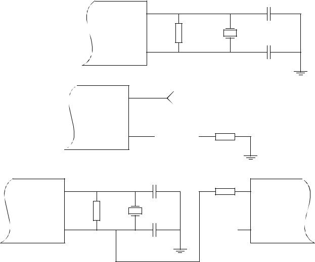
Pin Descriptions
Crystal driver and external clock input (XTAL, EXTAL)
In all cases, use caution when designing circuitry associated with the oscillator pins. Load capacitances shown in the oscillator circuits include all stray layout capacitances. See Figure 2-3.
|
|
EXTAL |
25 pF |
|
|
|
|
||
(a) Common crystal |
M68HC11 |
10 M¾ |
4•E |
|
connections |
crystal |
|||
|
|
|||
|
|
XTAL |
25 pF |
|
|
|
|
||
|
EXTAL |
External oscillator |
||
|
|
|||
(b) External oscillator |
M68HC11 |
|
|
|
connections |
|
|
||
|
|
|
||
|
|
NC or |
|
|
|
XTAL |
10–100k¾ load |
|
|
|
|
25 pF |
220¾ |
|
EXTAL |
|
|
|
EXTAL |
M68HC11 |
10 M¾ |
4•E |
|
M68HC11 |
crystal |
|
|||
XTAL |
|
25 pF |
NC or |
XTAL |
|
|
10–100k¾ |
|
|
|
|
|
load |
|
(c) One crystal driving two MCUs |
|
|
|
|
|
|
|
Note: capacitor values include all stray capacitance. |
|
Figure 2-3. Oscillator connections
MC68HC11P2 — |
Rev 1.0 |
Technical Data |
|
|
|
MOTOROLA |
Pin Descriptions |
25 |

Pin Descriptions
2.6 E clock output (E)
E is the output connection for the internally generated E clock. The signal from E is used as a timing reference. The frequency of the E clock output is one quarter that of the input frequency at the XTAL and EXTAL pins (except when the PLL is used as the clock source). When E clock output is low, an internal process is taking place; when it is high, data is being accessed. All clocks, including the E clock, are halted when the MCU is in STOP mode. The E clock output can be turned off in single chip modes to reduce the effects of RFI.
2.7 Phase-locked loop (XFC, VDDSYN)
|
The XFC and VDDSYN pins are the inputs for the on-chip PLL (phase- |
||
|
locked loop) circuitry. On reset all the device clocks are derived from the |
||
|
EXTAL input. The EXTAL clock is used as a reference for the PLL circuit, |
||
|
which generates a clock that is a multiple of the EXTAL frequency. Once |
||
|
the PLL has stabilized, alternate clocks may be selected. |
|
|
|
VDDSYN is the power supply pin for the PLL. Connecting it high enables |
||
|
the internal low frequency oscillator circuitry designed for the PLL. The |
||
|
PLL has been designed particularly for use with 614.4 and 640kHz |
||
|
crystals, though other values may be used. The maximum |
|
|
|
recommended crystal frequency for PLL operation is 2MHz. Above this |
||
|
frequency VDDSYN should be grounded to disable the PLL and enable |
||
|
the high frequency oscillator circuit; in this state EXTAL is designed for |
||
|
16MHz operation and XFC may be left unconnected. |
|
|
|
The PLL consists of a variable bandwidth loop filter, a voltage controlled |
||
|
oscillator (VCO), a feedback frequency divider and a digital phase |
||
|
detector. VDDSYN is the supply voltage for the PLL and must be suitably |
||
|
bypassed. The external capacitor on XFC should be located as close to |
||
|
the chip as possible to minimize noise. A typical value for this capacitor |
||
|
is 0.047µF, for a crystal frequency of 614.4kHz.(1) |
|
|
|
|
|
|
|
1. In general, a larger capacitor will improve the PLL’s frequency stability, at the expense of in- |
||
|
creasing the time required for it to settle (tPLLS) at the desired frequency. For a 32kHz appli- |
||
|
cation, or one in which the slew rate is not critical, a capacitor value of 0.1µF is usually |
||
|
adequate. For a crystal frequency of 614.4kHz and a slew time of 1–2ms (from 614kHz in |
||
|
WAIT mode to 16MHz in RUN mode), a capacitor of 0.047µF has been found satisfactory. |
||
Technical Data |
|
MC68HC11P2 — Rev 1.0 |
|
|
|
|
|
|
|
|
|
26 |
Pin Descriptions |
MOTOROLA |
|
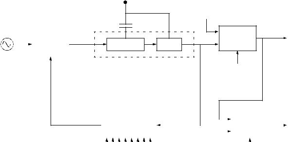
Pin Descriptions
Phase-locked loop (XFC, VDDSYN)
The PLL filter has two bandwidths that are automatically selected by the PLL, if the AUTO bit in PLLCR is set. Whenever the PLL is first enabled, the wide bandwidth mode is used. This enables the PLL frequency to ramp up quickly. When the output frequency is near the desired value, the filter is switched to the narrow bandwidth mode, to make the final frequency more stable. Manual control is possible, by clearing AUTO in PLLCR, and setting the appropriate value for BWC.
A block diagram of the PLL circuitry is given in Figure 2-4.
tREF |
|
Phase |
|
|
|
|
|
detect |
|
|
|
EXTAL
Low frequency crystal oscillator
|
VDDSYN |
|
|
|
|
|
EXTAL |
|
XFC |
|
4XCLK |
|
|
|
|
|
|
|
Bus clock |
PCOMP |
Loop filter |
VCO |
select |
|
To clock |
||
|
|
|
|
|
|
|
generation |
|
|
|
circuitry |
|
|
|
BCS |
tFB |
|
Frequency divider |
|
VCOOUT |
|
|
|
Module clock |
ST4XCK |
|||||||||
|
|
|
|
|
|
|
||||||||||||
|
|
|
|
|
|
|
|
|||||||||||
|
|
|
|
|
|
|
select |
For SCI |
||||||||||
|
|
|
|
|
|
|
|
|
|
|
|
|
|
|
||||
|
|
|
|
|
|
|
|
|
|
|
|
|
|
|
|
|
||
|
|
|
|
|
|
|
|
|
|
|
|
|
|
|
|
|
and timer |
|
|
|
|
|
|
|
|
|
|
|
|
|
|
|
|
|
|
||
|
|
|
|
|
|
|
|
|
|
|
|
EXTAL |
|
|||||
|
|
|
|
|
|
|
|
|
|
|
|
|
|
|
|
|
|
|
|
|
|
|
SYNR |
|
|
|
|
|
MCS |
||||||||
|
|
|
|
|
|
|
|
|
|
|
|
|
|
|
|
|
|
|
Figure 2-4. PLL circuit
2.7.1 Synchronization of PLL with subsystems
The timer and SCI subsystems operate off the EXTAL clock, but are accessed by the CPU relative to the internal PH2 signal. Although the EXTAL clock is used as the reference for the PLL, the PH2 clock and the module clocks for the timer and the SCI are not synchronized. In order to ensure synchronized data, special circuitry has been incorporated into both subsystems.
MC68HC11P2 — |
Rev 1.0 |
Technical Data |
|
|
|
MOTOROLA |
Pin Descriptions |
27 |

Pin Descriptions
2.7.2 Changing the PLL frequency
To change the PLL frequency it is necessary to perform the following sequence of events, in order to prevent possible bursts of high frequency operation during the reconfiguration of the PLL:
1.Switch to the low frequency bus rate (BCS = 0)
2.Disable the PLL (PLLON = 0)
3.Change the value in SYNR
4.Enable the PLL (PLLON = 1)
5.Wait a time tPLLS for the PLL frequency to stabilize
6.Switch to the high frequency bus rate (BCS = 1)
2.7.3 PLL registers
Two registers are used to control the operation of the MC68HC11P2 phase-locked loop circuitry. These are the PLL control register and the synthesizer program register, each of which is described below.
2.7.3.1 PLLCR — PLL control register
|
|
Address bit 7 |
bit 6 |
bit 5 |
bit 4 |
bit 3 |
bit 2 |
bit 1 |
bit 0 |
State |
|
|
|
on reset |
|||||||||
|
|
|
|
|
|
|
|
|
|
|
|
|
|
|
|
|
|
|
|
|
|
|
|
PLL control (PLLCR) |
$002E |
PLLON |
BCS |
AUTO |
BWC |
VCOT |
MCS |
LCK |
WEN |
1010 1000 |
|
|
|
|
|
|
|
|
|
|
|
|
|
This read/write register contains two bits that are used to enable and disable the synthesizer and to switch from slow (EXTAL) to one of the fast speeds. Two further bits are used to control the filter bandwidth. The SCI and timer clock source and the slow clock for WAIT mode are also controlled by this register.
PLLON — PLL on
1 = Switch PLL on.
0 = Switch PLL off.
Technical Data |
|
MC68HC11P2 — Rev 1.0 |
|
|
|
28 |
Pin Descriptions |
MOTOROLA |
Pin Descriptions
Phase-locked loop (XFC, VDDSYN)
This bit activates the synthesizer circuit without connecting it to the control circuit. This allows the circuit to stabilize before it drives the CPU clocks. PLLON is set by reset, to allow the control loop to stabilize during power up.
PLLON cannot be cleared whilst using VCOOUT to drive the internal processor clock, i.e. when BCS is set.
BCS — Bus clock select
1 = VCOOUT output drives the clock circuit (4XCLK). 0 = EXTAL drives the clock circuit (4XCLK).
This bit determines which signal drives the clock circuit generating the bus clocks. Once BCS has been altered it can take up to [1.5 EXTAL + 1.5 VCOOUT] cycles for the change in the clock to occur. Reset clears this bit.
NOTE: PLLON and BCS have built-in safeguards so that VCOOUT cannot be selected as the clock source (BCS = 1) if the PLL is off (PLLON = 0).
Similarly, the PLL cannot be turned off (PLLON = 0) if it is on and in use (BCS = 1). Turning the PLL on and selecting VCOOUT as the clock source therefore requires two independent writes to PLLCR.
AUTO — Automatic bandwidth control
1 = Automatic bandwidth control selected.
0 = Manual bandwidth control selected.
AUTO selects between automatic bandwidth control circuits in the phase detect block and manual bandwidth control. Reset sets this bit.
BWC — Bandwidth control
1 = High bandwidth control selected.
0 = Low bandwidth control selected.
Bandwidth control is under manual control only when AUTO is clear. (When AUTO is set, BWC acts as a read-only status bit to indicate which mode has been selected by the internal circuit.) A delay of tPLLS is required between changes to BWC. The low bandwidth driver is always enabled, so this bit determines whether the high bandwidth driver is on or off. On PLL start-up in automatic mode (AUTO = 1), the high bandwidth driver is enabled (BWC = 1) by internal circuitry until
MC68HC11P2 — |
Rev 1.0 |
Technical Data |
|
|
|
MOTOROLA |
Pin Descriptions |
29 |

Pin Descriptions
the PLL is near the specified frequency. The high bandwidth driver is then disabled and BWC is cleared by internal circuitry. Reset clears this bit.
Auto |
BWC |
High |
|
bandwidth |
|||
|
|
||
|
|
|
|
0 |
0 |
Off |
|
|
|
|
|
0 |
1 |
On |
|
|
|
|
|
1 |
X |
Auto |
|
|
|
|
VCOT — VCO test (Test mode only)
1 = Loop filter operates as specified by AUTO and BWC. 0 = Low bandwidth mode of the PLL filter is disabled.
This bit is used to isolate the loop filter from the VCO for testing purposes. VCOT is always set when AUTO = 1 when running in automatic mode. This bit is writable only in test mode. Reset sets this bit.
MCS — Module clock select
1 = 4XCLK is the source for the SCI and timer divider chain.
0 = EXTAL is the source for the SCI and timer divider chain.
Reset clears this bit.
LCK — Synthesizer lock detect 1 = The PLL has stabilized.
0 = The PLL is not stable.
This bit is used as an indicator for software that it is all right to set
BCS.
WEN — WAIT enable
1 = Low-power WAIT mode selected (PLL set to ‘idle’ in WAIT mode).
0 = Do not alter the 4XCLK during WAIT mode.
This bit determines whether the 4XCLK is disconnected from VCOOUT during WAIT and connected to EXTAL. Reset clears this bit.
When set, the CPU will respond to a WAIT instruction by first stacking the relevant registers, then by clearing BCS and setting the PLL to
‘idle’, with modulus = 1.
Technical Data |
|
MC68HC11P2 — Rev 1.0 |
|
|
|
30 |
Pin Descriptions |
MOTOROLA |
Loading...