Motorola MC12026AD, MC12026AP, MC12026BD, MC12026BP Datasheet

MOTOROLA
SEMICONDUCTOR TECHNICAL DATA
1.1GHz Dual Modulus Prescaler
The MC12026 is a high frequency, low voltage dual modulus prescaler used in phase±locked loop (PLL) applications.
The MC12026A can be used with CMOS synthesizers requiring positive edges to trigger internal counters such as Motorola's MC145xxx series in a PLL to provide tuning signals up to 1.1GHz in programmable frequency steps.
The MC12026B can be used with CMOS synthesizers requiring negative edges to trigger internal counters.
A Divide Ratio Control (SW) permits selection of an 8/9 or 16/17 divide ratio as desired.
The Modulus Control (MC) selects the proper divide number after SW has been biased to select the desired divide ratio.
NOTE: The ªBº Version Is Not Recommended for New Designs
•1.1GHz Toggle Frequency
•Supply Voltage 4.5V to 5.5V
•Low Power 4.0mA Typical
•Operating Temperature Range of ±40°C to +85°C
•The MC12026 is Pin Compatible With the MC12022
•Short Setup Time (tset ) 6ns Typical @ 1.1GHz
•Modulus Control Input Level is Compatible With Standard CMOS and TTL
Pinout: 8±Lead Plastic (Top View)
|
IN |
|
NC |
|
MC |
|
GND |
|
|
|
|
|
|
|
|
|
|
|
8 |
|
7 |
|
6 |
|
5 |
|
|
|
|
|
|
|
|
|
|
|
|
|
|
|
|
|
|
|
|
|
|
|
|
|
|
|
|
|
1 |
|
2 |
|
3 |
|
4 |
|
|
IN |
|
VCC |
SW |
|
OUT |
||
MAXIMUM RATINGS
MC12026A
MC12026B
MECL PLL COMPONENTS
8/9, 16/17
DUAL MODULUS PRESCALER
P SUFFIX
8±LEAD PLASTIC PACKAGE
CASE 626±05
D SUFFIX
8±LEAD PLASTIC SOIC PACKAGE
CASE 751±05
FUNCTION TABLE
SW |
MC |
Divide Ratio |
|
|
|
H |
H |
8 |
|
|
|
H |
L |
9 |
|
|
|
L |
H |
16 |
|
|
|
L |
L |
17 |
|
|
|
Note: SW: H = VCC, L = OPEN
MC: H = 2.0V to VCC; L = GND to 0.8V
Symbol |
Characteristic |
Range |
Unit |
|
|
|
|
VCC |
Power Supply Voltage, Pin 2 |
±0.5 to +7.0 |
Vdc |
TA |
Operating Temperature Range |
±40 to +85 |
°C |
Tstg |
Storage Temperature Range |
±65 to +150 |
°C |
MC |
Modulus Control Input, Pin 6 |
±0.5 to +6.5 |
Vdc |
|
|
|
|
IO |
Maximum Output Current, Pin 4 |
10.0 |
mA |
1/97
Motorola, Inc. 1997 |
1 |
REV 3 |

MC12026A MC12026B
ELECTRICAL CHARACTERISTICS (VCC = 4.5 to 5.5; TA = ±40 to +85°C)
Symbol |
Characteristic |
Min |
Typ |
Max |
Unit |
|
|
|
|
|
|
ft |
Toggle Frequency (Sin Wave) |
0.1 |
1.4 |
1.1 |
GHz |
ICC |
Supply Current Output Unloaded (Pin 2) |
Ð |
4.0 |
5.3 |
mA |
VIH1 |
Modulus Control Input High (MC) |
2.0 |
Ð |
VCC |
V |
VIL1 |
Modulus Control Input Low (MC) |
GND |
Ð |
0.8 |
V |
VIH2 |
Divide Ratio Control Input High (SW) |
VCC ± 0.5V |
VCC |
VCC + 0.5V |
V |
VIL2 |
Divide Ratio Control Input Low (SW) |
OPEN |
OPEN |
OPEN |
Ð |
Vout |
Output Voltage Swing |
1.0 |
1.6 |
Ð |
Vp±p |
|
(RL = 560Ω; IO = 5.5mA)1 |
|
|
|
|
|
(RL = 1.1kΩ; IO = 2.9mA)2 |
|
|
|
|
t |
Modulus Setup Time MC to Out3 |
Ð |
6 |
9 |
ns |
SET |
|
|
|
|
|
Vin |
Input Voltage Sensitivity |
|
|
|
mVpp |
|
100±250MHz |
400 |
Ð |
1000 |
|
|
250±1100MHz |
100 |
Ð |
1000 |
|
|
|
|
|
|
|
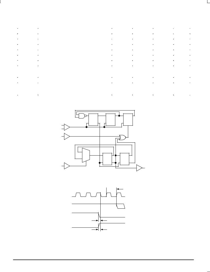
1.Divide Ratio of 8/9 at 1.1GHz, CL = 8pF
2.Divide Ratio of 16/17 at 1.1GHz, CL = 8pF
3.Assuming RL = 560Ω at 1.1GHz
D |
Q |
D |
Q |
|
D |
Q |
C |
QB |
C |
QB |
|
C |
QB |
|
M |
|||||
In |
|
|
|
|
|
|
In |
|
|
|
|
|
|
MC |
|
|
|
|
|
|
1 |
|
|
|
|
|
|
0 |
D |
QB |
|
D |
QB |
|
|
|
|
|
|
|
|
SW |
C |
Q |
|
C |
|
Q |
|
|
|
|
|
Out |
|
|
|
|
|
|
|
|
Figure 1. Logic Diagram (MC12026A)
Prop. Delay 
|
In |
|
Out |
MC Setup |
MC |
MC Release |
|
Modulus setup time MC to out is the MC setup or MC release plus the prop delay.
Figure 2. Modulus Setup Time
MOTOROLA |
2 |
HIPERCOMM |
|
|
BR1334 Ð Rev 4 |
 Loading...