


MC10H181FN

F
t
M is High C
M is Low C
is low
15
17
14
S0 S1 S2 S3
21
2
A0
F0
20
3
B0
18
A1
19
7
B1
F2
16
A2
11
B2
10
4
G
G
9
B3
225C
n
23 5MC
n+4
SEMICONDUCTOR TECHNICAL DATA
The MC10H181 is a high–speed arithmetic logic unit capable of performing
16 logic operations and 16 arithmetic operations on two four–bit words. Full
internal carry is incorporated for ripple through operation.
Arithmetic logic operations are selected by applying the appropriate binary
word to the select inputs (S0 through S3) as indicated in the tables of
arithmetic/logic functions. Group carry propagate (PG) and carry generate (GG)
are provided to allow fast operations on very long words using a second order
look–ahead. The internal carry is enabled by applying a low level voltage to the
mode control input (M).
When used with the MC10H179, full–carry look–ahead, as a second order
look–ahead block, the MC10H181 provides high–speed arithmetic operations
on very long words.
This 10H part is a functional/pinout duplication of the standard MECL 10K
family part with 100% improvement in propagation delay and no increase in
power supply current.
• Improved Noise Margin, 150 mV (Over Operating Voltage and
Temperature Range)
• Voltage Compensated • MECL 10K – Compatible
MAXIMUM RATINGS
Characteristic Symbol Rating Unit
Power Supply (VCC = 0) V
Input Voltage (VCC = 0) V
Output Current— Continuous
— Surge
Operating Temperature Range T
Storage Temperature Range— Plastic
— Ceramic
NOTE:
Each MECL 10H series circuit has been designed to meet the dc specifications shown in the test table,
after thermal equilibrium has been established. The circuit is in a test socket or mounted on a printed
circuit board and transverse air flow greater than 500 Ifpm is maintained. Outputs are terminated through
a 50–ohm resistor to –2.0 volts.
T
I
EE
I
out
A
stg
FUNCTION SELECT TABLE
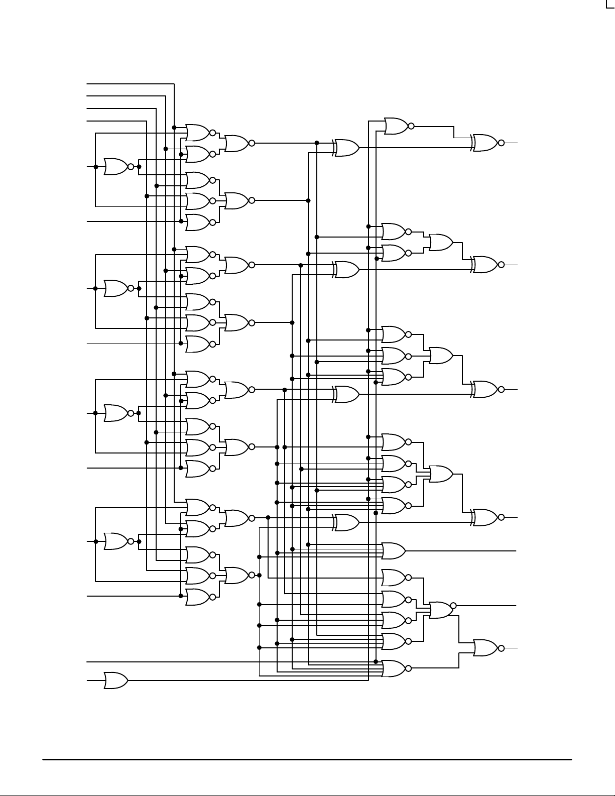
LOGIC DIAGRAM
13
15
17
14
21
20
18
19 7
16
11
10 4
9
22
23
S0 S1 S2 S3
A0
B0
A1
B1 F2
A2
B2
A3
B3
C
n
MC
G
n+4
F0
F1
F3
G
P
G
unction Selec
S3 S2 S1 S0
L L L L F = A F = A
L L L H F = A + B F = A plus (A • B)
L L H L F = A + B F = A plus (A • B)
L L H H F = Logical “1” F = A times 2
L H L L F = A • B F = (A + B) plus 0
L H L H F = B F = (A + B) plus (A • B)
2
L HHL
L H H H F = A + B F = A plus (A + B)
H LLL F = A • B F = (A + B) plus 0
H LLH
6
H L H L F = B F = (A + B) plus (A • B)
H L H H F = A + B F = A plus (A + B)
H H L L F = Logical “0” F = minus 1 (two’s complement)
8
H H L H F = A • B F = (A • B) minus 1
H H H L F = A • B F = (A • B) minus 1
H HHH F = A F = A minus 1
Logic Functions
M is Hi
h C = D.C.
F
F = AB
F = A B
= D.C.
–8.0 to 0 Vdc
0 to V
EE
50
100
0 to +75 °C
–55 to +150
–55 to +165
Arithmetic Operation
M is Low C
F = A plus B
F = A minus B minus 1
is low
n
F
Vdc
mA
°C
°C
L SUFFIX
CERAMIC PACKAGE
CASE 758–02
P SUFFIX
PLASTIC PACKAGE
CASE 724–03
FN SUFFIX
PLCC
CASE 776–02
DIP
PIN ASSIGNMENT
V
CC1
F0
F1
G
G
CN +
F3
F2
P
G
B3
A3
B2
V
EE
Pin assignment is for Dual–in–Line Package.
For PLCC pin assignment, see the Pin Conversion
T ables on page 6–11 of the Motorola MECL Data
4
Book (DL122/D).
1
2
3
4
5
6
7
8
9
10
11
12
24
23
22
21
20
19
18
17
16
15
14
13
V
M
C
A0
B0
B1
A1
S1
A2
S2
S0
S3
CC2
N
9/96
Motorola, Inc. 1996
2–275
REV 6
MC10H181
S3 13
S2 15
S1 17
S0 14
B0 20
A0 21
B1 19
A1 18
LOGIC DIAGRAM
2 F0
3 F1
B2 11
A2 16
B3 9
A3 10
Cn 22
7 F2
6 F3
8 P
4 G
5 C
G
G
n+4
M 23
V
= Pin 1
CC1
V
= Pin 24
CC2
VEE= Pin 12
MOTOROLA MECL Data
2–276
DL122 — Rev 6
 Loading...