


MC13280AYP
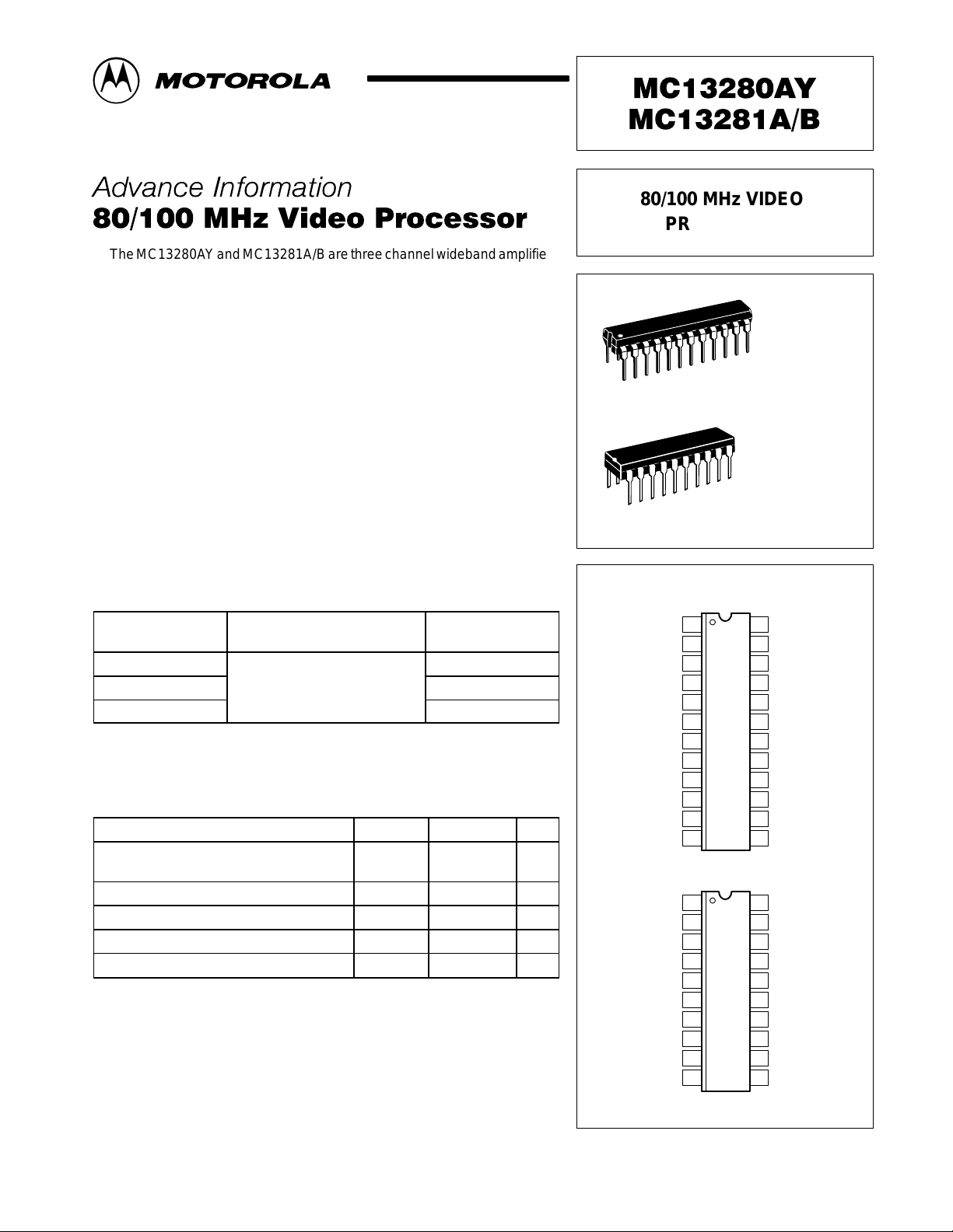
80/100 MHz VIDEO
PROCESSOR
P SUFFIX
PLASTIC PACKAGE
CASE 724
24
1
Order this document by MC13280A Y/D
PIN CONNECTIONS
124
23
22
21
20
19
18
17
2
3
4
5
6
7
8
(Top View)
R Subcontrast
R Input
G Subcontrast
B Input
Gnd
N/C
Blank
Video V
CC
16
15
14
13
9
10
11
12
N/C
N/C
N/C
Contrast
G Input
B Subcontrast
V
CC
Clamp
R Emitter
R Clamp
V5
G Emitter
G Clamp
Fast Commutate
B Clamp
B Emitter
P SUFFIX
PLASTIC PACKAGE
CASE 738
20
1
MC13281A
120
19
18
17
16
15
14
13
2
3
4
5
6
7
8
R Subcontrast
R Input
G Subcontrast
B Input
Gnd
V
CC
Blank
Video V
CC
12
11
9
10Fast Commutate
G Input
B Subcontrast
Contrast
Clamp
R Emitter
R Clamp
V5
G Emitter
G Clamp
B Clamp
B Emitter
MC13280AY
MC13281B
(Top View)
1
MOTOROLA ANALOG IC DEVICE DATA
The MC13280A Y and MC13281A/B are three channel wideband amplifiers
designed for use as a video pre–amplifier in high resolution RGB color
monitors.
Features:
• 4.0 Vpp Output Swing
• 3.5 ns Rise/Fall Time, 100 MHz Bandwidth (MC13281A/B)
• 4.3 ns Rise/Fall Time, 80 MHz Bandwidth (MC13280AY)
• Subcontrast Controls for Each Channel
• Main Contrast Control
• Blanking and Clamping Inputs
• Packages: NDIP–24 and NDIP–20
• A Single PC Board Pattern Can Accept the MC13281A and the
MC13282A (Video Amplifier with OSD)
ORDERING INFORMATION
Device
Operating
Temperature Range
Package
MC13280A YP Plastic DIP
MC13281AP
T
A
= 0° to +70°C
Plastic DIP
MC13281BP Plastic DIP
ABSOLUTE MAXIMUM RATINGS
Rating
Pin Value Unit
Power Supply Voltage V
CC
Video V
CC
–0.5, 10
–0.5, 10
Vdc
Voltage at Video Amplifier Inputs 2, 4, 6 –0.5, +5.0 Vdc
Collector–Emitter Current (Three Channels) Video V
CC
120 mA
Storage Temperature – –65 to +150 °C
Junction Temperature – 150 °C
NOTES: 1.Devices should not be operated at these limits. Refer to “Recommended
Operating Conditions” section for actual device operation.
2.ESD data available upon request.
This document contains information on a new product. Specifications and information herein
are subject to change without notice.
Motorola, Inc. 1996 Rev 0
MC13280AY MC13281A/B
2
MOTOROLA ANALOG IC DEVICE DATA
RECOMMENDED OPERATING CONDITIONS
Characteristic Pin Min Typ Max Unit
Power Supply Voltage V
CC
,
Video V
CC
7.6 8.0 8.4 Vdc
Contrast Control Contrast 0 – 5.0 Vdc
Subcontrast Control 1, 3, 5 0 – 5.0 Vdc
Blanking Input Signal Amplitude Blank 0 – 5.0 V
Clamping Input Signal Amplitude Clamp 0 – 5.0 V
Video Signal Amplitude
(with 75 Ω Termination)
2, 4, 6 – 0.7 1.0 Vpp
Collector–Emitter Current (Total for Three
Channels)
Video V
CC
0 – 50 mA
Clamp Pulse Width Clamp 500 – – ns
Operating Ambient Temperature – 0 – 70 °C
ELECTRICAL CHARACTERISTICS (Refer to Test Circuit Figure 1, T
A
= 25°C, V
CC
= 8.0 Vdc.)
Characteristic Condition Pin Min Typ Max Unit
Input Impedance
– 2, 4, 6
100 – – kΩ
Internal DC Bias Voltage
– 2.4 – Vdc
Output Signal Amplitude
V2, V4, V6 = 0.7 Vpp
R, G, B
3.6 4.0 – Vpp
Voltage Gain
V1
,
V3
,
V5
=
5
.
0
V
Contrast = 5.0 V
E
m
itt
ers
– 5.6 – V/V
Contrast Control Contrast = 5.0 to 0 V
V1, V3, V5 = 5.0 V
Contrast – –26 – dB
Subcontrast Control V1, V3, V5 = 5.0 to 0 V
Contrast = 5.0 V
1, 3, 5 – –26 – dB
Emitter DC Level – – 1.0 1.2 1.4 Vdc
Blanking Input Threshold – Blank – 1.25 – V
Clamping Input Threshold – Clamp – 3.75 – V
Video Rise Time
MC13280A Y
MC13281A/B
V2, V4, V6 = 0.7 Vpp
V
out
= 4.0 Vpp
R
L
> 300 Ω, C
L
< 5.0 pF
R, G, B
Emitters
–
–
4.3
3.5
–
–
ns
Video Fall Time
MC13280A Y
MC13281A/B
V2, V4, V6 = 0.7 Vpp
V
out
= 4.0 Vpp
R
L
> 300 Ω, C
L
< 5.0 pF
R, G, B
Emitters –
–
4.3
3.5
–
–
ns
Video Bandwidth
MC13280A Y
MC13281A/B
V2, V4, V6 = 0.7 Vpp
V1, V3, V5, Contrast = 5.0 V
R
L
> 300 Ω, C
L
< 5.0 pF
R, G, B
Emitters –
–
80
100
–
–
MHz
Power Supply Current V
CC
, Video V
CC
= 8.0 V – – 70 – mA
NOTE: It is recommended to use a double sided PCB layout for high frequency measurement (e.g., rise/fall time, bandwidth).

MC13280AY MC13281A/B
3
MOTOROLA ANALOG IC DEVICE DATA
Figure 1. Internal Block Diagram
Fast Commutate
R Input
R Subcontrast
Contrast
G Input
G Subcontrast
B Input
B Subcontrast
R Clamp
Video V
CC
R Emitter
G Clamp
G Emitter
Blank
Clamp
B Clamp
B Emitter
V
CC
V5
Gnd
V
ref1
V
ref1
V
ref1
V
ref2
V
ref2
V
ref2
R Channel
G Channel
B Channel
Clamp Blank
Decoder
Contrast and Subcontrast
Control Processor
Contrast and Subcontrast
Control Processor
Contrast and Subcontrast
Control Processor
This device contains 272 active transistors.
MC13280AY MC13281A/B
4
MOTOROLA ANALOG IC DEVICE DATA
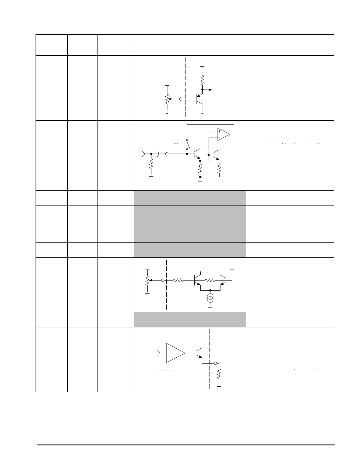
PIN FUNCTION DESCRIPTION
MC13280AY
MC13281B
Pin
MC13281A
Pin
Name Equivalent Internal Circuit Description
1 1 R
Subcontrast
Control
V
CC
These pins provides a maximum of
26 dB attenuation to vary the gain of
each video amplifier separately.
3 3 G
Subcontrast
Control
5.0 V
50 k
Input voltage is from 0 to 5.0 V .
Increasing the voltage will increase
the contrast level.
5 5 B
Subcontrast
Control
2 2 R Input
5.0 V
V
ref
The input coupling capacitor is used
for input clamping storage. The
maximum source impedance is 100 Ω.
4 4 G Input
5
.
0
V
Clamp
75
Ω
0.1
Input polarity of the video signal is
positive.
Nominal 0.7 Vpp input signal is
6 6 B Input
1.0 k10 k
recommen
d
e
d
(
max
i
mum
1
.
0
V
pp
)
.
7 7 Ground Ground pin. Connect to a clean, solid
ground.
N/A 8 N/C
Connected to ground.
10 N/C
11 N/C
12 N/C
8 9 V
CC
Connect to 8.0 Vdc supply, ±5%.
Decoupling is required at this pin.
9 13 Contrast
2.5 V
42 k
5.0 V
2.0 k
Overall Contrast Control for the three
channels.
The input range is 0 V to 5.0 V. An
increase of voltage increases the
contrast.
10 14 Fast
Commutate
Must be connected to ground.
11 15 B Emitter
Output
V
CC
The video outputs are configured as
emitter–followers with a driving
capability of about 15 mA each.
15 19 G Emitter
Output
Video
Signal
The dc voltage at these three emitters
is set to 1.2 V (black level).
The dc current through the output
18 22 R Emitter
Output
R
E
=
330
Typical
Contrast
The dc current through the output
stage is determined by the emitter
resistors (typically 330 Ω).
 Loading...