


MOTOROLA
SEMICONDUCTOR TECHNICAL DATA
Quad |
Bus |
Driver/Receiver |
with |
|
|
|
|
||||||||
2-to-1 |
Output |
Multiplexers |
|
|
MC10H330 |
||||||||||
|
|
|
|
|
|
|
|
|
|
|
|||||
The MC10H330 is a Quad Bus Driver/Receiver with two±to±one output |
|
|
|
|
|||||||||||
multiplexers. These multiplexers have a common select and output enable. |
|
|
|
|
|||||||||||
When disabled, (OE = high) the bus outputs go to ±2.0 V. Their output can be |
|
|
|
|
|||||||||||
brought to a low state (VOL) by applying a high level to the receiver enable (RE |
|
|
|
|
|||||||||||
= High). The parameters specified are with 25 Ω loading on the bus drivers and |
|
|
|
|
|||||||||||
50 Ω loads on the receivers. |
|
|
|
|
|
|
|
|
|
|
L SUFFIX |
||||
• Propagation Delay, 1.5 ns Typical Data±to±Output |
|
|
|
|
|
|
CERAMIC PACKAGE |
||||||||
• Improved Noise Margin 150 mV (Over Operating Voltage and |
|
|
CASE 758±02 |
||||||||||||
|
|
|
|
||||||||||||
Temperature Range) |
|
|
|
|
|
|
|
|
|
|
|
|
|||
• Voltage Compensated |
|
|
|
|
|
|
|
|
|
|
P SUFFIX |
||||
• MECL 10K±Compatible |
|
|
|
|
|
|
|
|
|
|
|||||
|
|
|
|
|
|
|
|
|
|
PLASTIC PACKAGE |
|||||
|
|
|
|
|
|
|
|
|
|
|
|
|
|||
MAXIMUM RATINGS |
|
|
|
|
|
|
|
|
|
|
|
CASE 724±03 |
|||
|
|
|
|
|
|
|
|
|
|
|
|
|
|||
Characteristic |
|
|
Symbol |
|
Rating |
|
|
Unit |
|
|
FN SUFFIX |
||||
Power Supply (VCC = 0) |
|
|
|
VEE |
|
±8.0 to 0 |
|
|
Vdc |
|
|
PLCC |
|
||
|
|
|
|
|
|
|
|
CASE 776±02 |
|||||||
Input Voltage (VCC = 0) |
|
|
|
VI |
|
0 to VEE |
|
|
Vdc |
|
|
|
|
||
Output Current Ð Continuous |
|
|
Iout |
|
50 |
|
|
mA |
|
|
DIP |
|
|||
Ð Surge |
|
|
|
|
|
100 |
|
|
|
|
|
|
|||
Operating Temperature Range |
|
|
TA |
|
0 to +75 |
|
|
°C |
|
PIN ASSIGNMENT |
|
||||
|
|
|
|
|
|
|
|
|
|||||||
Storage Temperature Range Ð Plastic |
|
Tstg |
±55 to +150 |
|
°C |
|
|
|
|
||||||
|
|
Ð Ceramic |
|
|
±55 to +165 |
|
°C |
VCC |
1 |
24 |
VCC0 |
||||
ELECTRICAL CHARACTERISTICS (VEE = ±5.2 V ±5%) (See Note) |
|
|
XBUS |
2 |
23 |
YBUS |
|||||||||
|
|
|
0° |
25° |
75° |
|
|
WBUS |
3 |
22 |
ZBUS |
||||
Characteristic |
Symbol |
Min |
Max |
Min |
Max |
Min |
Max |
|
Unit |
||||||
|
|
|
|
|
|||||||||||
Power Supply Current |
IE |
Ð |
157 |
Ð |
143 |
Ð |
157 |
|
mA |
VCC0 |
4 |
21 |
OE |
||
|
|
IinH |
|
|
|
|
|
|
|
μ |
X1 |
|
|
Y0 |
|
Input Current High |
|
|
|
|
|
|
|
|
A |
5 |
20 |
|
|||
Pins 5±8, 17±20 |
|
|
Ð |
667 |
Ð |
417 |
Ð |
417 |
|
|
X0 |
6 |
19 |
Y1 |
|
Pins 16, 21 |
|
|
Ð |
514 |
Ð |
321 |
Ð |
321 |
|
|
|||||
Pin 9 |
|
|
Ð |
475 |
Ð |
297 |
Ð |
297 |
|
|
W1 |
7 |
18 |
Z0 |
|
Input Current Low |
|
IinL |
0.5 |
Ð |
0.5 |
Ð |
0.3 |
Ð |
|
μA |
|||||
|
|
W0 |
8 |
17 |
Z1 |
||||||||||
High Output Voltage |
VOH |
±1.02 |
±0.84 |
±0.98 |
±0.81 |
±0.92 |
±0.735 |
Vdc |
|||||||
|
|
|
|
||||||||||||
Low Output Voltage |
VOL |
±1.95 |
±1.63 |
±1.95 |
±1.63 |
±1.95 |
±1.60 |
|
Vdc |
S |
9 |
16 |
RE |
||
High Input Voltage |
|
VIH |
±1.17 |
±0.84 |
±1.13 |
±0.81 |
±1.07 |
±0.735 |
Vdc |
WIN |
10 |
15 |
ZIN |
||
Low Input Voltage |
|
VIL |
±1.95 |
±1.48 |
±1.95 |
±1.48 |
±1.95 |
±1.45 |
|
Vdc |
XIN |
11 |
14 |
YIN |
|
AC PARAMETERS |
|
|
|
|
|
|
|
|
|
||||||
|
|
|
|
|
|
|
|
|
VEE |
12 |
13 |
VCC0 |
|||
Propagation Delay |
tpd |
|
|
|
|
|
|
|
ns |
||||||
Select±to±Input |
|
|
1.8 |
5.3 |
1.8 |
5.3 |
1.8 |
5.3 |
|
|
Pin assignment is for Dual±in±Line Package. |
||||
Data±to±Bus Output |
|
0.5 |
2.0 |
0.5 |
2.0 |
0.5 |
2.0 |
|
|
||||||
|
|
|
For PLCC pin assignment, see the Pin Conversion |
||||||||||||
Select±to±Bus |
|
|
|
|
|
|
|
|
|
|
|||||
|
|
|
|
|
|
|
|
|
|
Tables on page 6±11 of the Motorola MECL Data |
|||||
Output |
|
|
1.0 |
3.2 |
1.0 |
3.2 |
1.0 |
3.2 |
|
|
|||||
|
|
|
|
|
Book (DL122/D). |
|
|||||||||
OE±to±Bus Output |
|
0.8 |
2.2 |
0.8 |
2.2 |
0.8 |
2.2 |
|
|
|
|
||||
|
|
|
|
|
|
|
|||||||||
Bus±to±Input |
|
|
0.8 |
2.1 |
0.8 |
2.1 |
0.8 |
2.4 |
|
|
NOTE: |
|
|
|
|
RE±to±Input |
|
|
0.5 |
2.2 |
0.5 |
2.2 |
0.5 |
2.2 |
|
|
|
|
|
||
|
|
|
|
Each MECL 10H series circuit has been designed |
|||||||||||
Data±to±Receiver |
|
|
|
|
|
|
|
|
|
to meet the dc specifications shown in the test table, |
|||||
Input |
|
|
1.3 |
4.0 |
1.3 |
4.0 |
1.3 |
4.0 |
|
|
after thermal equilibrium has been established. The |
||||
Rise Time |
|
tr |
0.5 |
2.0 |
0.5 |
2.0 |
0.5 |
2.0 |
|
ns |
circuit is in a test socket or mounted on a printed |
||||
|
|
circuit board and transverse air flow greater than |
|||||||||||||
Fall Time |
|
tf |
0.5 |
2.0 |
0.5 |
2.0 |
0.5 |
2.0 |
|
ns |
500 Ifpm is maintained. Receiver outputs are |
||||
|
|
terminated through a 50±ohm resistor to ±2.0 volts |
|||||||||||||
dc. Bus outputs are terminated through a 25±ohm resistor to ±2.0 volts dc.
3/93
Motorola, Inc. 1996 |
2±299 |
REV 5 |
MC10H330
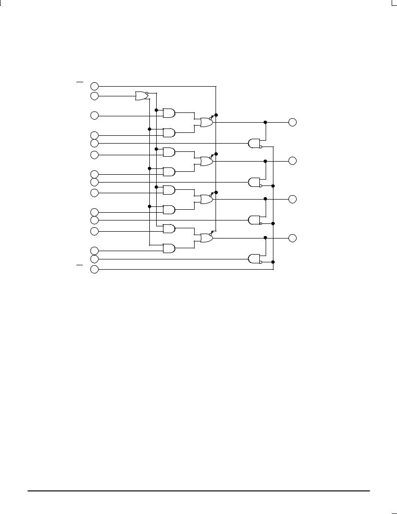
LOGIC DIAGRAM
OE |
21 |
VCC0 |
= |
PIN 24 |
|
S |
9 |
VCC |
= |
PIN 1 |
|
VCC0 |
= |
PIN 13 |
|
||
|
|
|
|||
|
|
VCC0 |
= |
PIN 4 |
|
W0 |
8 |
VEE |
= |
PIN 12 |
|
|
|
|
|
||
|
|
|
|
3 |
WBUS |
W1 |
7 |
|
|
|
|
WIN |
10 |
|
|
|
|
X0 |
6 |
|
|
|
XBUS |
|
|
|
|
2 |
|
X1 |
5 |
|
|
|
|
XIN |
11 |
|
|
|
|
Y0 |
20 |
|
|
|
|
|
|
|
|
23 |
YBUS |
Y1 |
19 |
|
|
|
|
YIN |
14 |
|
|
|
|
Z0 |
18 |
|
|
|
|
|
|
|
|
22 |
ZBUS |
Z1 |
17 |
|
|
|
|
ZIN |
15 |
|
|
|
|
RE |
16 |
|
|
|
|
MULTIPLEXER TRUTH TABLE
OE |
S |
|
WBus |
XBus |
YBus |
ZBus |
|
|
|
|
|
|
|
H |
X |
|
±2.0 V |
±2.0 V |
±2.0 V |
±2.0 V |
L |
L |
|
W0 |
X0 |
Y0 |
Z0 |
L |
H |
|
W1 |
X1 |
Y1 |
Z1 |
|
|
|
|
|
|
|
RECEIVER TRUTH TABLE
RE |
|
Win |
Xin |
Yin |
Zin |
|
|
|
|
|
|
|
|
H |
|
L |
L |
L |
L |
|
L |
|
WBus |
XBus |
YBus |
ZBus |
|
MOTOROLA |
2±300 |
MECL Data |
|
|
DL122 Ð Rev 6 |
 Loading...