


Motorola MC14025UBCL, MC14025UBCP, MC14025UBD, MC14023UBCL, MC14023UBCP Datasheet
...
MOTOROLA
SEMICONDUCTOR TECHNICAL DATA
|
|
MC14001UB |
|
|
|
|
Quad 2-Input NOR Gate |
||
UB-Suffix Series CMOS Gates |
|
MC14002UB |
|
|
The UB Series logic gates are constructed with P and N channel |
|
Dual 4-Input NOR |
Gate |
|
enhancement mode devices in a single monolithic structure (Complemen- |
|
MC14011UB |
|
|
tary MOS). Their primary use is where low power dissipation and/or high |
|
|
|
|
|
|
|
|
|
noise immunity is desired. The UB set of CMOS gates are inverting |
|
Quad 2-Input NAND |
Gate |
|
non±buffered functions. |
|
|||
• Supply Voltage Range = 3.0 Vdc to 18 Vdc |
|
MC14012UB |
|
|
• Linear and Oscillator Applications |
|
|
|
|
• Capable of Driving Two Low±power TTL Loads or One Low±power |
|
Dual 4-Input NAND |
Gate |
|
Schottky TTL Load Over the Rated Temperature Range |
|
MC14023UB |
|
|
• Double Diode Protection on All Inputs |
|
|
|
|
|
|
|
|
|
• Pin±for±Pin Replacements for Corresponding CD4000 Series UB Suffix |
|
Triple 3-Input NAND |
Gate |
|
Devices |
|
|||
|
|
|
|
|
|
|
MC14025UB |
|
|
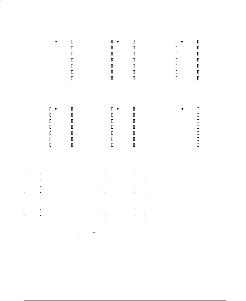
LOGIC DIAGRAMS |
|
Triple 3-Input NOR |
Gate |
|
|
|
|
|
|
|
MC14001UB |
|
MC14002UB |
|
MC14011UB |
|
Quad 2±Input |
|
Dual 4±Input |
|
Quad 2±Input |
|
NOR Gate |
|
NOR Gate |
|
NAND Gate |
1 |
3 |
2 |
|
|
1 |
2 |
3 |
|
|
3 |
|
|
|
1 |
2 |
||
5 |
|
4 |
|
5 |
|
4 |
|
|
|||
6 |
|
|
|
4 |
|
|
5 |
|
|
6 |
|
8 |
10 |
9 |
|
|
8 |
9 |
10 |
|
|
10 |
|
|
|
13 |
9 |
||
12 |
|
11 |
|
12 |
|
11 |
|
|
|||
13 |
12 |
|
|
11 |
|
|
NC = 6, 8 |
|
13 |
||
|
|
|
|
|
|
MC14012UB |
MC14023UB |
|
|
MC14025UB |
|
Dual 4±Input |
Triple 3±Input |
|
|
Triple 3±Input |
|
NAND Gate |
NAND Gate |
|
|
NOR Gate |
2 |
|
1 |
|
1 |
|
|
2 |
9 |
2 |
9 |
|
3 |
|
||||
1 |
8 |
|
8 |
|
|
4 |
|
|
|||
|
3 |
|
3 |
|
|
5 |
|
|
|
||
|
4 |
6 |
4 |
6 |
|
9 |
|
||||
|
5 |
|
5 |
|
|
10 |
13 |
|
|
||
11 |
|
11 |
|
||
11 |
|
|
|||
|
12 |
10 |
12 |
10 |
|
12 |
|
||||
NC = 6, 8 |
13 |
|
13 |
|
|
|
|
|
VDD = PIN 14
VSS = PIN 7
FOR ALL DEVICES
L SUFFIX
CERAMIC
CASE 632
P SUFFIX
PLASTIC
CASE 646
D SUFFIX
SOIC
CASE 751A
ORDERING INFORMATION
MC14XXXUBCP |
Plastic |
MC14XXXUBCL |
Ceramic |
MC14XXXUBD |
SOIC |
TA = ± 55° to 125°C for all packages.
This device contains protection circuitry to guard against damage due to high static voltages or electric fields. However, precautions must be taken to avoid applications of any voltage higher than maximum rated voltages to this high±impedance circuit. For proper operation, Vin and Vout should be constrained
to the range VSS v (Vin or Vout) v VDD. Unused inputs must always be tied to an
appropriate logic voltage level (e.g., either VSS or VDD). Unused outputs must be left open.
REV 3 1/94
Motorola, Inc. 1995
PIN ASSIGNMENTS
|
MC14001UB |
|
|
MC14002UB |
|
|
MC14011UB |
|
|||||
Quad 2±Input NOR Gate |
Dual 4±Input NOR Gate |
Quad 2±Input NAND Gate |
|||||||||||
IN 1A |
|
|
VDD |
OUTA |
|
|
|
VDD |
|
|
|
|
|
|
1 |
14 |
1 |
14 |
|
IN 1A |
1 |
14 |
VDD |
||||
|
|
||||||||||||
|
|||||||||||||
IN 2A |
|
2 |
13 |
IN 2D |
IN 1A |
2 |
13 |
|
OUTB |
IN 2A |
2 |
13 |
IN 2D |
|
|||||||||||||
OUTA |
|
3 |
12 |
IN 1D |
IN 2A |
3 |
12 |
|
IN 4B |
OUTA |
3 |
12 |
IN 1D |
|
|||||||||||||
OUTB |
|
4 |
11 |
OUTD |
IN 3A |
4 |
11 |
|
IN 3B |
OUTB |
4 |
11 |
OUTD |
|
|||||||||||||
IN 1B |
|
5 |
10 |
OUTC |
IN 4A |
5 |
10 |
|
IN 2B |
IN 1B |
5 |
10 |
OUTC |
|
|||||||||||||
IN 2B |
|
6 |
9 |
IN 2C |
NC |
6 |
9 |
|
IN 1B |
IN 2B |
6 |
9 |
IN 2C |
|
|||||||||||||
VSS |
|
7 |
8 |
IN 1C |
VSS |
7 |
8 |
|
NC |
VSS |
7 |
8 |
IN 1C |
|
|||||||||||||
|
|
|
MC14012UB |
|
|
|
|
MC14023UB |
|
|
|
|
MC14025UB |
|
|||||||
|
Dual 4±Input NAND Gate |
Triple 3±Input NAND Gate |
Triple 3±Input NOR Gate |
||||||||||||||||||
|
|
|
|
|
|
|
|
|
|
|
|
|
|
|
|
|
|
|
|
|
|
|
|
|
|
|
|
|
|
|
|
|
|
|
|
|
|
|
|
|
|
|
|
|
|
OUTA |
|
1 |
14 |
|
VDD |
|
IN 1A |
|
1 |
14 |
VDD |
IN 1A |
|
1 |
14 |
|
VDD |
||
|
|
|
|
|
|
|
|||||||||||||||
|
|
IN 1A |
|
2 |
13 |
|
OUTB |
|
IN 2A |
|
2 |
13 |
IN 3C |
IN 2A |
|
2 |
13 |
|
IN 3C |
||
|
|
|
|
|
|
|
|||||||||||||||
|
|
IN 2A |
|
3 |
12 |
|
IN 4B |
|
IN 1B |
|
3 |
12 |
IN 2C |
IN 1B |
|
3 |
12 |
|
IN 2C |
||
|
|
|
|
|
|
|
|||||||||||||||
|
|
IN 3A |
|
4 |
11 |
|
IN 3B |
|
IN 2B |
|
4 |
11 |
IN 1C |
IN 2B |
|
4 |
11 |
|
IN 1C |
||
|
|
|
|
|
|
|
|||||||||||||||
|
|
IN 4A |
|
5 |
10 |
|
IN 2B |
|
IN 3B |
|
5 |
10 |
OUTC |
IN 3B |
|
5 |
10 |
|
OUTC |
||
|
|
|
|
|
|
|
|||||||||||||||
|
|
NC |
|
6 |
9 |
|
IN 1B |
|
OUTB |
|
6 |
9 |
OUTA |
OUTB |
|
6 |
9 |
|
OUTA |
||
|
|
|
|
|
|
|
|||||||||||||||
|
|
VSS |
|
7 |
8 |
|
NC |
|
|
VSS |
|
7 |
8 |
IN 3A |
VSS |
|
7 |
8 |
|
IN 3A |
|
|
|
|
|
|
|
|
|||||||||||||||
|
|
|
|
|
|
|
|
|
|
|
NC = NO CONNECTION |
|
|
|
|
|
|
||||
MAXIMUM RATINGS* (Voltages Referenced to VSS) |
|
|
|
|
|
|
|
|
|
|
|
||||||||||
|
|
|
|
|
|
|
|
|
|
|
|
|
|
|
|
|
|
|
|
||
Symbol |
|
|
|
|
Parameter |
|
|
|
|
Value |
|
Unit |
|
|
|
|
|
|
|
||
|
|
|
|
|
|
|
|
|
|
|
|
|
|
|
|||||||
VDD |
|
DC Supply Voltage |
|
|
|
± 0.5 to + 18.0 |
V |
|
|
|
|
|
|
|
|||||||
Vin, Vout |
|
Input or Output Voltage (DC or Transient) |
|
|
± 0.5 to VDD + 0.5 |
V |
|
|
|
|
|
|
|
||||||||
lin, lout |
|
Input or Output Current (DC or Transient), |
|
|
± 10 |
|
mA |
|
|
|
|
|
|
|
|||||||
|
|
per Pin |
|
|
|
|
|
|
|
|
|
|
|
|
|
|
|
|
|
||
|
|
|
|
|
|
|
|
|
|
|
|
|
|
|
|
||||||
PD |
|
Power Dissipation, per Package² |
|
|
|
500 |
|
mW |
|
|
|
|
|
|
|
||||||
Tstg |
|
Storage Temperature |
|
|
|
± 65 to + 150 |
|
_C |
|
|
|
|
|
|
|
||||||
TL |
|
Lead Temperature (8±Second Soldering) |
|
|
|
260 |
|
_C |
|
|
|
|
|
|
|
||||||
* Maximum Ratings are those values beyond which damage to the device may occur. ²Temperature Derating:
Plastic ªP and D/DWº Packages: ± 7.0 mW/C From 65_C To 125_C Ceramic ªLº Packages: ± 12 mW/C From 100_C To 125_C
MOTOROLA CMOS LOGIC DATA |
MC14001UB |
|
19 |

ELECTRICAL CHARACTERISTICS (Voltages Referenced to VSS)
|
|
|
VDD |
± 55_C |
|
25_C |
|
125_C |
|
||
|
|
|
|
|
|
|
|
|
|
|
|
Characteristic |
|
Symbol |
Vdc |
Min |
Max |
Min |
Typ # |
Max |
Min |
Max |
Unit |
|
|
|
|
|
|
|
|
|
|
|
|
Output Voltage |
ª0º Level |
VOL |
5.0 |
Ð |
0.05 |
Ð |
0 |
0.05 |
Ð |
0.05 |
Vdc |
Vin = VDD or 0 |
|
|
10 |
Ð |
0.05 |
Ð |
0 |
0.05 |
Ð |
0.05 |
|
|
|
|
15 |
Ð |
0.05 |
Ð |
0 |
0.05 |
Ð |
0.05 |
|
|
|
|
|
|
|
|
|
|
|
|
|
Vin = 0 or VDD |
ª1º Level |
VOH |
5.0 |
4.95 |
Ð |
4.95 |
5.0 |
Ð |
4.95 |
Ð |
Vdc |
|
|
|
10 |
9.95 |
Ð |
9.95 |
10 |
Ð |
9.95 |
Ð |
|
|
|
|
15 |
14.95 |
Ð |
14.95 |
15 |
Ð |
14.95 |
Ð |
|
|
|
|
|
|
|
|
|
|
|
|
|
Input Voltage |
ª0º Level |
VIL |
|
|
|
|
|
|
|
|
Vdc |
(VO = 4.5 Vdc) |
|
|
5.0 |
Ð |
1.0 |
Ð |
2.25 |
1.0 |
Ð |
1.0 |
|
(VO = 9.0 Vdc) |
|
|
10 |
Ð |
2.0 |
Ð |
4.50 |
2.0 |
Ð |
2.0 |
|
(VO = 13.5 Vdc) |
|
|
15 |
Ð |
2.5 |
Ð |
6.75 |
2.5 |
Ð |
2.5 |
|
(VO = 0.5 Vdc) |
ª1º Level |
IIH |
5.0 |
4.0 |
Ð |
4.0 |
2.75 |
Ð |
4.0 |
Ð |
Vdc |
(VO = 1.0 Vdc) |
|
|
10 |
8.0 |
Ð |
8.0 |
5.50 |
Ð |
8.0 |
Ð |
|
(VO = 1.5 Vdc) |
|
|
15 |
12.5 |
Ð |
12.5 |
8.25 |
Ð |
12.5 |
Ð |
|
Output Drive Current |
|
IOH |
|
|
|
|
|
|
|
|
mAdc |
(VOH = 2.5 Vdc) |
Source |
|
5.0 |
± 1.2 |
Ð |
± 1.0 |
± 1.7 |
Ð |
± 0.7 |
Ð |
|
(VOH = 4.6 Vdc) |
|
|
5.0 |
± 0.25 |
Ð |
± 0.2 |
± 0.36 |
Ð |
± 0.14 |
Ð |
|
(VOH = 9.5 Vdc) |
|
|
10 |
± 0.62 |
Ð |
± 0.5 |
± 0.9 |
Ð |
± 0.35 |
Ð |
|
(VOH = 13.5 Vdc) |
|
|
15 |
± 1.8 |
Ð |
± 1.5 |
± 3.5 |
Ð |
± 1.1 |
Ð |
|
(VOL = 0.4 Vdc) |
Sink |
IOL |
5.0 |
0.64 |
Ð |
0.51 |
0.88 |
Ð |
0.36 |
Ð |
mAdc |
(VOL = 0.5 Vdc) |
|
|
10 |
1.6 |
Ð |
1.3 |
2.25 |
Ð |
0.9 |
Ð |
|
(VOL = 1.5 Vdc) |
|
|
15 |
4.2 |
Ð |
3.4 |
8.8 |
Ð |
2.4 |
Ð |
|
Input Current |
|
Iin |
15 |
Ð |
± 0.1 |
Ð |
± 0.00001 |
± 0.1 |
Ð |
± 1.0 |
μAdc |
Input Capacitance |
|
Cin |
Ð |
Ð |
Ð |
Ð |
5.0 |
7.5 |
Ð |
Ð |
pF |
(Vin = 0) |
|
|
|
|
|
|
|
|
|
|
|
Quiescent Current |
|
IDD |
5.0 |
Ð |
0.25 |
Ð |
0.0005 |
0.25 |
Ð |
7.5 |
μAdc |
(Per Package) |
|
|
10 |
Ð |
0.5 |
Ð |
0.0010 |
0.5 |
Ð |
15 |
|
|
|
|
15 |
Ð |
1.0 |
Ð |
0.0015 |
1.0 |
Ð |
30 |
|
|
|
|
|
|
|
|
|
|
|
|
|
Total Supply Current**² |
|
IT |
5.0 |
|
|
IT = (0.3 μA/kHz) f + IDD/N |
|
|
μAdc |
||
(Dynamic plus Quiescent, |
|
10 |
|
|
IT = (0.6 μA/kHz) f + IDD/N |
|
|
|
|||
Per Gate CL = 50 pF) |
|
|
15 |
|
|
IT = (0.8 μA/kHz) f + IDD/N |
|
|
|
||
#Data labelled ªTypº is not to be used for design purposes but is intended as an indication of the IC's potential performance. ** The formulas given are for the typical characteristics only at 25_C.
²T o calculate total supply current at loads other than 50 pF: IT(CL) = IT(50 pF) + (CL ± 50) Vfk
where: IT is in μH (per package), CL in pF, V = (VDD ± VSS) in volts, f in kHz is input frequency, and k = 0.001 x the number of exercised gates per package.
MC14001UB |
MOTOROLA CMOS LOGIC DATA |
20 |
|
 Loading...