


MOTOROLA MC10H176MR1, MC10H176M, MC10H176MEL, MC10H176ML1, MC10H176ML2 Datasheet
...
MOTOROLA
SEMICONDUCTOR TECHNICAL DATA
Hex D Master-Slave Flip-Flop
The MC10H176 contains six master slave type D flip±flops with a common clock. This MECL 10H part is a functional/pinout duplication of the standard MECL 10K family part, with 100% improvement in clock frequency and propagation delay and no increase in power±supply current.
•Propagation Delay, 1.7 ns Typical
•Power Dissipation, 460 mW Typical
•Improved Noise Margin 150 mV (Over Operating Voltage and Temperature Range)
•Voltage Compensated
•MECL 10K±Compatible
MAXIMUM RATINGS
Characteristic |
Symbol |
Rating |
Unit |
|
|
|
|
Power Supply (VCC = 0) |
VEE |
±8.0 to 0 |
Vdc |
Input Voltage (VCC = 0) |
VI |
0 to VEE |
Vdc |
Output Current Ð Continuous |
Iout |
50 |
mA |
Ð Surge |
|
100 |
|
|
|
|
|
Operating Temperature Range |
TA |
0 to +75 |
°C |
Storage Temperature Range Ð Plastic |
Tstg |
±55 to +150 |
°C |
Ð Ceramic |
|
±55 to +165 |
°C |
|
|
|
|
ELECTRICAL CHARACTERISTICS (VEE = ±5.2 V ±5%) (See Note)
|
|
0° |
25° |
|
75° |
|
|||
|
|
|
|
|
|
|
|
|
|
Characteristic |
Symbol |
Min |
Max |
Min |
Max |
Min |
|
Max |
Unit |
|
|
|
|
|
|
|
|
|
|
Power Supply Current |
IE |
Ð |
123 |
Ð |
112 |
Ð |
|
123 |
mA |
Input Current High |
IinH |
|
|
|
|
|
|
|
μA |
Pins 5,6,7,10,11,12 |
|
Ð |
425 |
Ð |
265 |
Ð |
|
265 |
|
Pin 9 |
|
Ð |
670 |
Ð |
420 |
Ð |
|
420 |
|
|
|
|
|
|
|
|
|
|
|
Input Current Low |
IinL |
0.5 |
Ð |
0.5 |
Ð |
0.3 |
|
Ð |
μA |
High Output Voltage |
VOH |
±1.02 |
±0.84 |
±0.98 |
±0.81 |
±0.92 |
|
±0.735 |
Vdc |
Low Output Voltage |
VOL |
±1.95 |
±1.63 |
±1.95 |
±1.63 |
±1.95 |
|
±1.60 |
Vdc |
High Input Voltage |
VIH |
±1.17 |
±0.84 |
±1.13 |
±0.81 |
±1.07 |
|
±0.735 |
Vdc |
Low Input Voltage |
VIL |
±1.95 |
±1.48 |
±1.95 |
±1.48 |
±1.95 |
|
±1.45 |
Vdc |
AC PARAMETERS |
|
|
|
|
|
|
|
|
|
|
|
|
|
|
|
|
|
|
|
Propagation Delay |
tpd |
0.9 |
2.1 |
0.9 |
2.2 |
1.0 |
|
2.4 |
ns |
Set±up Time |
tset |
1.5 |
Ð |
1.5 |
Ð |
1.5 |
|
Ð |
ns |
Hold Time |
thold |
0.9 |
Ð |
0.9 |
Ð |
1.0 |
|
Ð |
ns |
Rise Time |
tr |
0.5 |
1.8 |
0.5 |
1.9 |
0.5 |
|
2.0 |
ns |
Fall Time |
tf |
0.5 |
1.8 |
0.5 |
1.9 |
0.5 |
|
2.0 |
ns |
Toggle Frequency |
ftog |
250 |
Ð |
250 |
Ð |
250 |
|
Ð |
MHz |
NOTE:
Each MECL 10H series circuit has been designed to meet the dc specifications shown in the test table, after thermal equilibrium has been established. The circuit is in a test socket or mounted on a printed circuit board and transverse air flow greater than 500 linear fpm is maintained. Outputs are terminated through a 50±ohm resistor to ±2.0 volts.
MC10H176
L SUFFIX
CERAMIC PACKAGE
CASE 620±10
P SUFFIX
PLASTIC PACKAGE
CASE 648±08
FN SUFFIX
PLCC
CASE 775±02
CLOCKED TRUTH TABLE
C |
Q |
Qn+1 |
L |
X |
Qn |
H * |
L |
L |
H * |
H |
H |
*A clock H is a clock transition from a low to a high state.
DIP
PIN ASSIGNMENT
VCC1 |
|
1 |
|
16 |
|
VCC2 |
|
|
|
||||
Q0 |
|
2 |
|
15 |
|
Q5 |
|
|
|
||||
Q1 |
|
3 |
|
14 |
|
Q4 |
|
|
|
||||
Q2 |
|
4 |
|
13 |
|
Q3 |
|
|
|
||||
D0 |
|
5 |
|
12 |
|
D5 |
|
|
|
||||
D1 |
|
6 |
|
11 |
|
D4 |
|
|
|
||||
D2 |
|
7 |
|
10 |
|
D3 |
|
|
|
||||
VEE |
|
8 |
|
9 |
|
CLOCK |
|
|
|
||||
|
|
|
|
|
|
|
Pin assignment is for Dual±in±Line Package. For PLCC pin assignment, see the Pin Conversion Tables on page 6±11 of the Motorola MECL Data Book (DL122/D).
3/93
Motorola, Inc. 1996 |
2±113 |
REV 5 |
MC10H176
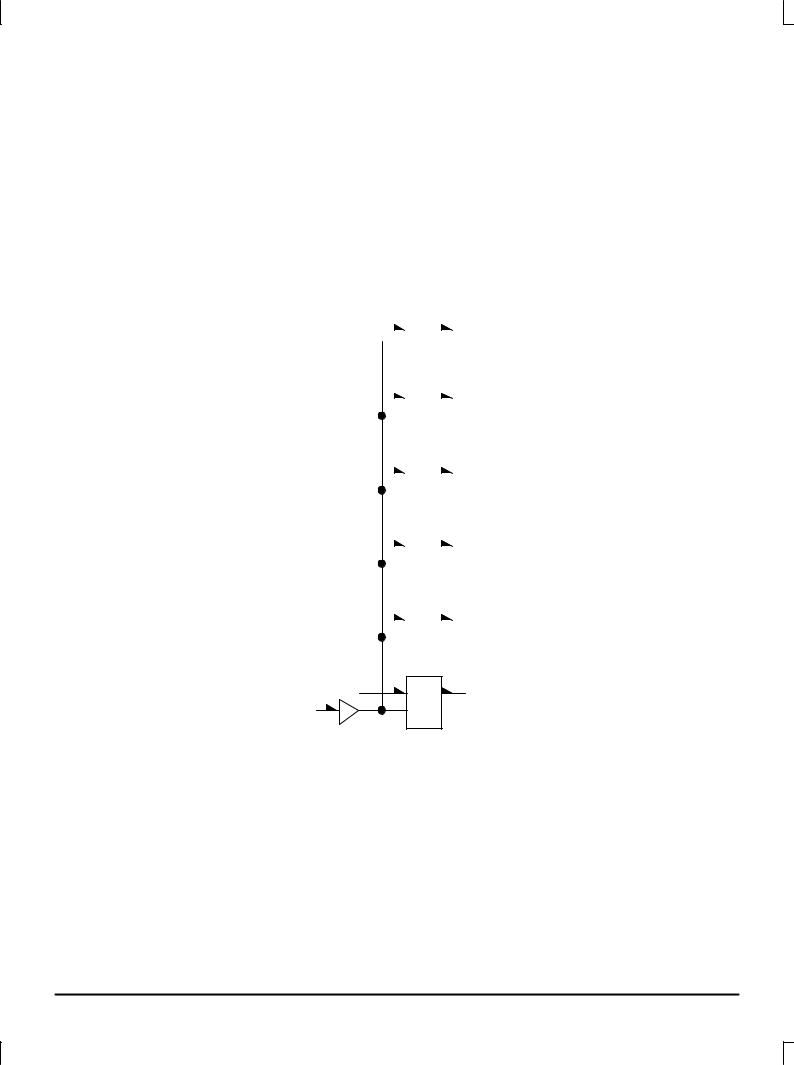
APPLICATION INFORMATION
The MC10H176 contains six high±speed, master slave type ªDº flip±flops. Data is entered into the master when the clock is low. Master±to±slave data transfer takes place on the positive±going Clock transition. Thus,
outputs may change only on a positive±going Clock transition. A change in the information present at the data
(D) input will not affect the output information any other time due to the master±slave construction of this device.
LOGIC DIAGRAM
D0 |
5 |
|
|
|
|
2 |
Q0 |
|
|
|
|||||
|
|
|
|
|
|
|
|
|
|
|
|
|
|
|
|
D1 |
6 |
|
|
|
|
3 |
Q1 |
|
|
|
|
||||
|
|
|
|
|
|
|
|
|
|
|
|
|
|
|
|
D2 |
7 |
|
|
|
|
4 |
Q2 |
|
|
|
|
||||
|
|
|
|
|
|
|
|
|
|
|
|
|
|
|
|
D3 |
10 |
|
|
|
|
13 |
Q3 |
|
|
|
|
||||
|
|
|
|
|
|
|
|
|
|
|
|
|
|
|
|
D4 |
11 |
|
|
|
|
14 |
Q4 |
|
|
|
|
||||
|
|
|
|
|
|
|
|
|
|
|
|
|
|
|
|
D5 |
12 |
15 |
Q5 |
CLOCK |
9 |
|
|
VCC1 = PIN 1
VCC2 = PIN 16
VEE = PIN 8
MOTOROLA |
2±114 |
MECL Data |
|
|
DL122 Ð Rev 6 |
 Loading...