


MC14094BCP
MOTOROLA CMOS LOGIC DATA
1
MC14094B
The MC14094B combines an 8–stage shift register with a data latch for
each stage and a three–state output from each latch.
Data is shifted on the p ositive clock transition and is shifted from the
seventh stage to two serial o utputs. The Q
S
output data is f or use in
high–speed c ascaded systems. The Q′
S
output data is shifted on the
following negative clock transition for use in low–speed cascaded systems.
Data from each stage of the shift register is latched on the negative
transition of the strobe input. Data propagates through the latch while strobe
is high.
Outputs of the eight data latches are controlled by three–state buffers
which are placed in the high–impedance state by a logic Low on Output
Enable.
• Three–State Outputs
• Capable of Driving Two Low–Power TTL Loads or One Low–Power
Schottky TTL Load Over the Rated Temperature Range
• Input Diode Protection
• Data Latch
• Dual Outputs for Data Out on Both Positive and Negative Clock
Transitions
• Useful for Serial–to–Parallel Data Conversion
• Pin–for–Pin Compatible with CD4094B
MAXIMUM RATINGS* (Voltages Referenced to V
SS
)
Symbol
Parameter
Value
Unit
V
DD
DC Supply Voltage
– 0.5 to + 18.0
V
V
in
, V
out
Input or Output Voltage (DC or Transient)
– 0.5 to V
DD
+ 0.5
V
I
in
, I
out
Input or Output Current (DC or Transient),
per Pin
± 10
mA
P
D
Power Dissipation, per Package†
500
mW
T
stg
Storage Temperature
– 65 to + 150
_
C
T
L
Lead Temperature (8–Second Soldering)
260
_
C
*Maximum Ratings are those values beyond which damage to the device may occur.
†Temperature Derating:
Plastic “P and D/DW” Packages: – 7.0 mW/
_
C From 65
_
C To 125
_
C
Ceramic “L” Packages: – 12 mW/
_
C From 100
_
C To 125
_
C
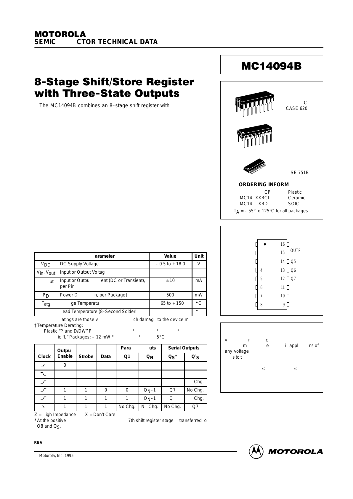
Output
Parallel Outputs Serial Outputs
Clock
Output
Enable
Strobe
Data
Q1 Q
N
Q
S
* Q′
S
0 X X Z Z Q7 No Chg.
0 X X Z Z No Chg. Q7
1 0 X No Chg. No Chg. Q7 No Chg.
1 1 0 0 Q
N
–1 Q7 No Chg.
1 1 1 1 Q
N
–1 Q7 No Chg.
1 1 1 No Chg. No Chg. No Chg. Q7
Z = High Impedance X = Don’t Care
*At the positive clock edge, information in the 7th shift register stage is transferred to
Q8 and Q
S
.
SEMICONDUCTOR TECHNICAL DATA
Motorola, Inc. 1995
REV 3
1/94
L SUFFIX
CERAMIC
CASE 620
ORDERING INFORMATION
MC14XXXBCP Plastic
MC14XXXBCL Ceramic
MC14XXXBD SOIC
T
A
= – 55° to 125°C for all packages.
P SUFFIX
PLASTIC
CASE 648
D SUFFIX
SOIC
CASE 751B
13
14
15
16
9
10
11
125
4
3
2
1
8
7
6
Q7
Q6
Q5
OUTPUT
ENABLE
V
DD
Q
S
Q
′
S
Q8
Q1
CLOCK
DATA
STROBE
V
SS
Q4
Q3
Q2
PIN ASSIGNMENT
This device contains protection circuitry to
guard against damage due to high static
voltages or electric fields. However, pre-
cautions must be taken to avoid applications of
any voltage higher than maximum rated volt-
ages to this high–impedance circuit. For proper
operation, V
in
and V
out
should be constrained
to the range V
SS
v
(V
in
or V
out
)
v
V
DD
.
Unused inputs must always be tied to an
appropriate logic voltage level (e.g., either V
SS
or V
DD
). Unused outputs must be left open.
MOTOROLA CMOS LOGIC DATAMC14094B
2
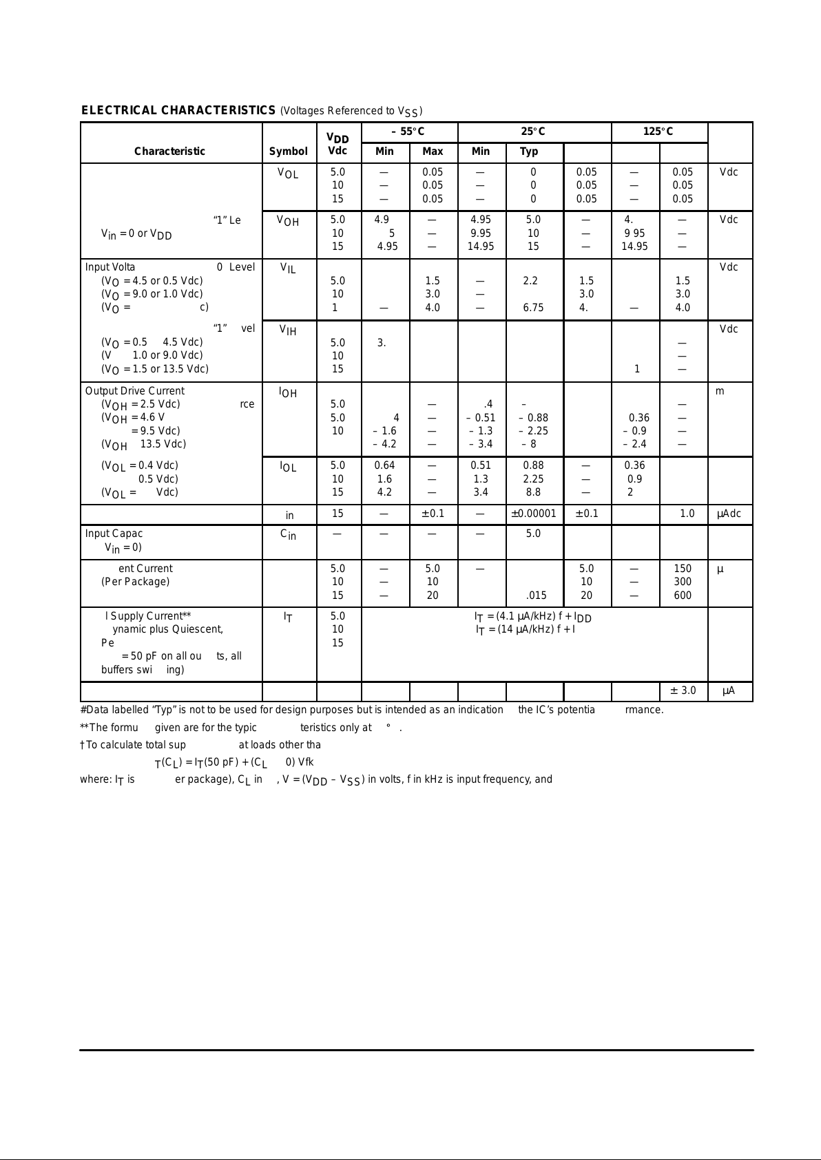
ELECTRICAL CHARACTERISTICS (Voltages Referenced to V
SS
)
V
– 55
_
C
25
_
C
125
_
C
Characteristic
Symbol
V
DD
Vdc
Min
Max
Min
Typ #
Max
Min
ÎÎÎ
ÎÎÎ
ÎÎÎ
Max
Unit
Output Voltage
“0” Level
V
in
= V
DD
or 0
V
OL
5.0
10
15
—
—
—
0.05
0.05
0.05
—
—
—
0
0
0
0.05
0.05
0.05
—
—
—
ÎÎÎ
ÎÎÎ
ÎÎÎ
ÎÎÎ
0.05
0.05
0.05
Vdc
“1” Level
V
in
= 0 or V
DD
V
OH
5.0
10
15
4.95
9.95
14.95
—
—
—
4.95
9.95
14.95
5.0
10
15
—
—
—
4.95
9.95
14.95
ÎÎÎ
ÎÎÎ
ÎÎÎ
ÎÎÎ
ÎÎÎ
—
—
—
Vdc
Input Voltage
“0” Level
(V
O
= 4.5 or 0.5 Vdc)
(V
O
= 9.0 or 1.0 Vdc)
(V
O
= 13.5 or 1.5 Vdc)
V
IL
5.0
10
15
—
—
—
1.5
3.0
4.0
—
—
—
2.25
4.50
6.75
1.5
3.0
4.0
—
—
—
ÎÎÎ
ÎÎÎ
ÎÎÎ
ÎÎÎ
ÎÎÎ
1.5
3.0
4.0
Vdc
“1” Level
(V
O
= 0.5 or 4.5 Vdc)
(V
O
= 1.0 or 9.0 Vdc)
(V
O
= 1.5 or 13.5 Vdc)
V
IH
5.0
10
15
3.5
7.0
11
—
—
—
3.5
7.0
11
2.75
5.50
8.25
—
—
—
3.5
7.0
11
ÎÎÎ
ÎÎÎ
ÎÎÎ
ÎÎÎ
ÎÎÎ
—
—
—
Vdc
Output Drive Current
(V
OH
= 2.5 Vdc) Source
(V
OH
= 4.6 Vdc)
(V
OH
= 9.5 Vdc)
(V
OH
= 13.5 Vdc)
I
OH
5.0
5.0
10
15
– 3.0
– 0.64
– 1.6
– 4.2
—
—
—
—
– 2.4
– 0.51
– 1.3
– 3.4
– 4.2
– 0.88
– 2.25
– 8.8
—
—
—
—
– 1.7
– 0.36
– 0.9
– 2.4
ÎÎÎ
ÎÎÎ
ÎÎÎ
ÎÎÎ
ÎÎÎ
—
—
—
—
mAdc
(V
OL
= 0.4 Vdc) Sink
(V
OL
= 0.5 Vdc)
(V
OL
= 1.5 Vdc)
I
OL
5.0
10
15
0.64
1.6
4.2
—
—
—
0.51
1.3
3.4
0.88
2.25
8.8
—
—
—
0.36
0.9
2.4
ÎÎÎ
ÎÎÎ
ÎÎÎ
ÎÎÎ
ÎÎÎ
—
—
—
mAdc
Input Current
I
in
15
—
± 0.1
—
±0.00001
± 0.1
—
ÎÎÎ
ÎÎÎ
ÎÎÎ
± 1.0
µAdc
Input Capacitance
(V
in
= 0)
C
in
—
—
—
—
5.0
7.5
—
ÎÎÎ
ÎÎÎ
ÎÎÎ
—
pF
Quiescent Current
(Per Package)
I
DD
5.0
10
15
—
—
—
5.0
10
20
—
—
—
0.005
0.010
0.015
5.0
10
20
—
—
—
ÎÎÎ
ÎÎÎ
ÎÎÎ
ÎÎÎ
ÎÎÎ
150
300
600
µAdc
Total Supply Current**†
(Dynamic plus Quiescent,
Per Package)
(C
L
= 50 pF on all outputs, all
buffers switching)
I
T
5.0
10
15
I
T
= (4.1 µA/kHz) f + I
DD
I
T
= (14 µA/kHz) f + I
DD
I
T
= (140 µA/kHz) f + I
DD
µAdc
3–State Output Leakage Current
I
TL
15
—
± 0.1
—
± 0.0001
± 0.1
—
ÎÎÎ
ÎÎÎ
ÎÎÎ
± 3.0
µA
#Data labelled “Typ” is not to be used for design purposes but is intended as an indication of the IC’s potential performance.
**The formulas given are for the typical characteristics only at 25
_
C.
†To calculate total supply current at loads other than 50 pF:
I
T
(C
L
) = I
T
(50 pF) + (C
L
– 50) Vfk
where: I
T
is in µA (per package), C
L
in pF, V = (V
DD
– V
SS
) in volts, f in kHz is input frequency, and k = 0.001.
 Loading...