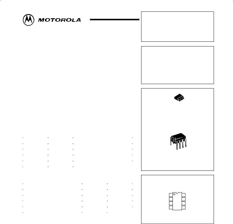
Motorola MC12022LVAD, MC12022LVAP, MC12022LVBD, MC12022LVBP Datasheet

Order this document by MC12022LVA/D
1.1 GHz Low-Voltage
Dual Modulus Prescaler
The MC12022LVA can be used with CMOS synthesizers requiring positive edges to trigger internal counters such as Motorola's MC145XXX series in a PLL to provide tuning signals up to 1.1 GHz in programmable frequency steps.
The MC12022LVB can be used with CMOS synthesizers requiring negative edges to trigger internal counters.
A Divide Ratio Control (SW) permits selection of a 64/65 or 128/129 divide ratio as desired.
The Modulus Control (MC) selects the proper divide number after SW has been biased to select the desired divide ratio.
NOTE: The ªBº Version Is Not Recommended for New Designs
•1.1 GHz Toggle Frequency
•Supply Voltage of 2.7 to 5.0 V
•Low±Power 4.0 mA Typical at VCC = 2.7 V
•Operating Temperature Range of ±40 to 85°C
•Short Setup Time (tset) 16ns Maximum @ 1.1 GHz
•Modulus Control Input Level Is Compatible With Standard CMOS and TTL
FUNCTIONAL TABLE
SW |
MC |
Divide Ratio |
|
|
|
H |
H |
64 |
|
|
|
H |
L |
65 |
|
|
|
L |
H |
128 |
|
|
|
L |
L |
129 |
|
|
|
NOTES: 1. SW: H = VCC, L = Open. A logic L can also be applied by grouunding this pin, but this is not recommended due to increased power soncumption.
2. MC: H = 2.0 V to VCC, L = GND to 0.8 V.
DESIGN GUIDE
Criteria |
Value |
Unit |
|
|
|
Internal Gate Count* |
67 |
ea |
|
|
|
Internal Gate Propagation Delay |
200 |
ps |
|
|
|
Internal Gate Power Dissipation |
0.75 |
mW |
|
|
|
Speed Power Product |
0.15 |
pJ |
|
|
|
NOTE: * Equivalent to a two±input NAND gate
MC12022LVA
MC12022LVB
MECL PLL COMPONENTS64/65, 128/129
DUAL MODULUS PRESCALER
SEMICONDUCTOR
TECHNICAL DATA
8 

1
D SUFFIX
PLASTIC PACKAGE
CASE 751 (SO±8)
8
1
P SUFFIX
PLASTIC PACKAGE
CASE 626
PIN CONNECTIONS
IN |
1 |
8 |
IN |
|
V |
2 |
7 |
NC |
|
CC |
|
|
|
|
SW 3 |
6 |
MC |
||
OUT |
4 |
5 |
Gnd |
|
|
|
(Top View) |
|
|
ORDERING INFORMATION
|
Operating |
|
Device |
Temp Range |
Package |
|
|
|
MC12022LVAD |
|
SO±8 |
|
|
|
MC12022LVAP |
TA = |
Plastic |
MC12022LVBD |
± 40° to +85°C |
SO±8 |
|
||
|
|
|
MC12022LVBP |
|
Plastic |
|
|
|
Motorola, Inc. 1997 |
Rev 3 |

MC12022LVA MC12022LVB
MAXIMUM RATINGS
Rating |
Symbol |
Value |
Unit |
|
|
|
|
Power Supply Voltage, Pin 2 |
VCC |
±0.5 to 7.0 |
Vdc |
Operating Temperature Range |
TA |
±40 to 85 |
°C |
Storage Temperature Range |
Tstg |
±65 to 150 |
°C |
Modulus Control Input, Pin 6 |
MC |
±0.5 to 6.5 |
Vdc |
|
|
|
|
NOTE; ESD data available upon request.
ELECTRICAL CHARACTERISTICS (VCC = 4.5 to 5.5 V; TA = ±40°C to 85°C, unless otherwise noted.)
Characteristic |
Symbol |
Min |
Typ |
Max |
Unit |
|
|
|
|
|
|
Toggle Frequency (Sine Wave Input) |
ft |
0.1 |
1.4 |
1.1 |
GHz |
Supply Current Output Unloaded (Pin 2) |
ICC |
± |
4.7 |
6.5 |
mA |
Supply Current Output Unloaded (Pin 2) at 5.0 Vdc |
ICCH |
|
5.8 |
8.0 |
mA |
Modulus Control Input High (MC) |
VIH1 |
2.0 |
± |
VCC |
V |
Modulus Control Input Low (MC) |
VIL1 |
± |
± |
0.8 |
V |
Divide Ratio Control Input High (SW) |
VIH2 |
VCC |
VCC |
VCC |
Vdc |
Divide Ratio Control Input Low (SW) |
VIL2 |
Open |
Open |
Open |
± |
Output Voltage Swing (CL = 12 pF; RL = 1.1 kΩ at 2.7 Vdc) |
Vout |
0.8 |
1.0 |
± |
Vpp |
Output Voltage Swing (CL = 12 pF; RL = 2.2 kΩ at 5.0 Vdc) |
Vout |
1.0 |
1.6 |
± |
Vpp |
Modulus Setup Time MC to Out |
tset |
± |
11 |
16 |
ns |
Input Voltage Sensitivity 250±1100 MHz |
Vin(min) |
100 |
± |
1500 |
mVpp |
100±250 MHz |
|
400 |
± |
1500 |
|
|
|
|
|
|
|
Output Current (CL = 12 pF; RL = 2.2 kΩ at 2.7 Vdc) |
IO |
± |
1.2 |
4.0 |
mA |
Output Current (CL = 12 pF; RL = 2.2 kΩ at 5.0 Vdc) |
IO |
± |
1.2 |
4.0 |
mA |
2 |
MOTOROLA RF/IF DEVICE DATA |

MC12022LVA MC12022LVB
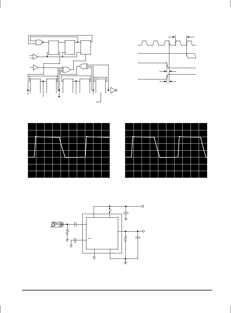
Figure 1. Logic Diagram (MC12022LVA) |
Figure 2. Modulus Setup Time |
|
|
|
|
|
|
|
|
|
|
Prop. Delay |
|
|
|
D |
Q |
D |
Q |
D |
Q |
|
|
|
In |
|
|
|
A |
|
B |
|
C |
|
|
|
|
|
|
|
|
|
|
C |
QB |
|
|
|
|
In |
|
C |
QB |
C |
QB |
M |
|
|
|
Out |
|
|
|
|
|
|
|
|
|
|
|
||
In |
|
|
|
|
|
|
|
|
|
|
|
MC |
|
|
|
|
|
|
|
|
|
|
|
|
|
|
|
|
|
|
|
|
|
MC Setup |
MC |
D |
Q |
D |
QB |
D |
Q |
D |
QB |
D |
QB |
MC Release |
|
|
D |
E |
F |
|
|
G |
|
H |
|
|
|
|
C QB |
|
|
|
C |
Q |
|
|
|
|
|
C QB |
|
|
C Q |
|
|
|
|
|
|
C S |
Q |
|
|
|
|
Out |
Modulus setup time MC to out is the MC |
|||
|
|
|
|
|
|
|
|
|
|
|
|
|
|
|
|
|
|
|
|
|
|
|
|
|
|
|
|
|
|
|
|
setup or MC release plus the prop delay. |
|
|
|
|
|
|
|
|
|
|
|
|
|
|
|
|
|
|
|
|
|
|
|
|
|
|
|
|
|
|
|
|
|
|
|
|
|
|
|
|
|
|
|
|
|
|
|
|
|
|
|
|
|
|
|
|
|
|
|
|
|
|
|
|
|
|
SW 
Figure 3. Typical Output Waveforms
500 m ≈ |
20 ns |
( 64, 500MHz Input Frequency, VCC = 5.0V, TA = 25°C, Output Loaded) |
|
500 m ≈ |
20 ns |
( 128, 1.1GHz Input Frequency, VCC = 5.0V, TA = 25°C, Output Loaded) |
|
|
|
Figure 4. AC Test Circuit |
|
|
|
|
|
|
VCC = 2.7 to 5.0Vdc |
|
|
C3 |
|
|
Sine Wave Generator |
VCC |
SW |
|
|
C1 |
|
|
||
IN |
|
|
|
|
|
|
|
|
|
50Ω |
|
OUT |
|
|
C2 |
IN |
RL |
CL |
EXTERNAL COMPONENTS |
|
|
|
|
C1 = C2 = 1000pF |
|
MC |
GND |
|
C3 = 0.1μF |
|
|
CL = 12pF (Including Scope |
||
|
|
|
|
|
|
|
|
|
and jig capacitance) |
|
|
|
|
RL = 2.2kΩ (at +5.0Vdc) |
|
MC Input |
|
RL = 1.1kΩ (at +2.7Vdc) |
|
|
|
|
||
MOTOROLA RF/IF DEVICE DATA |
3 |
|
 Loading...