Motorola MC12015D, MC12015P, MC12016D, MC12016P, MC12017D Datasheet
...
Order this document by MC12015/D
MC12015 MC12016 MC12017
Dual Modulus Prescaler
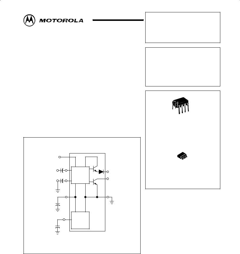
The MC12015, MC12016 and MC12017 are dual modulus prescalers which will drive divide by 32 and 33, 40 and 41, and 64 and 65, respectively. An internal regulator is provided to allow these devices to be used over a wide range of power±supply voltages. The devices may be operated by applying a supply voltage of 5.0 Vdc ±10% at Pin 7, or by applying an unregulated voltage source from 5.5Vdc to 9.5 Vdc to Pin 8.
•225 MHz Toggle Frequency
•Low±Power 7.5 mA Maximum at 6.8 V
•Control Input and Output Are Compatible With Standard CMOS
•Connecting Pins 2 and 3 Allows Driving One TTL Load
•Supply Voltage 4.5 V to 9.5 V
SIMPLIFIED BLOCK DIAGRAM
Control |
|
|
|
|
Input |
reg |
|
|
1 |
|
|
|
V |
|
|
|
0.001μF |
TO |
|
Signal |
|
2 Active |
|
|
|
||
Input |
5 |
N / N+1 |
Pullup |
|
|||
Signal |
6 |
|
Output |
GND |
0.001μF |
|
3 |
|
|
|
|
|
Vreg |
|
4 |
|
7 |
|
|
|
0.1μF |
|
GND |
|
|
|
|
|
VCC |
Voltage |
|
|
|
|
|
|
8 |
Regulator |
|
|
0.1μF |
|
|
1.Vreg at Pin 7 is not guaranteed to be between 4.5 and
5.5V when VCC is being applied to Pin 8
2.Pin 7 is not to be used as a source of regulated output
voltage
MECL PLL COMPONENTS DUAL MODULUS PRESCALER
SEMICONDUCTOR
TECHNICAL DATA
8
1
P SUFFIX
PLASTIC PACKAGE
CASE 626
8 

1
D SUFFIX
PLASTIC PACKAGE
CASE 751
(SO±8)
ORDERING INFORMATION
|
|
Operating |
|
Device |
Temperature Range |
Package |
|
|
|
|
|
MC12015D |
|
|
|
|
|
|
|
MC12016D |
|
SO±8 |
|
|
|
|
|
MC12017D |
TA = ±40° to +85°C |
|
|
|
|
|
|
MC12015P |
|
||
|
|
||
|
|
|
|
MC12016P |
|
Plastic |
|
|
|
|
|
MC12017P |
|
|
|
|
|
|
|
Motorola, Inc. 1997 |
Rev 2 |

MC12015 MC12016 MC12017
MAXIMUM RATINGS [tblhead]
Rating |
Symbol |
Value |
|
Unit |
|
|
|
|
||
|
|
|
|
|
|
|
|
|
|
|
Regulated Voltage, Pin 7 |
Vreg |
8.0 |
|
Vdc |
|
|
|
|
||
Power Supply Voltage, Pin 8 |
VCC |
10 |
|
Vdc |
|
|
|
|
||
Operating Temperature Range |
TA |
±40 to +85 |
|
°C |
|
|
|
|
||
Storage Temperature Range |
Tstg |
±65 to +175 |
|
°C |
|
|
|
|
||
NOTE: ESD data available upon request. |
|
|
|
|
|
|
|
|
|
|
ELECTRICAL CHARACTERISTICS (VCC = 5.5 to 9.5 V; Vreg = 4.5 to 5.5 V; TA = ±40 to 85°C, unless otherwise noted.) |
|
|||||||||
Characteristic |
|
|
Symbol |
|
Min |
Typ |
Max |
Unit |
||
|
|
|
|
|
|
|
|
|
|
|
Toggle Frequency (Sine Wave Input) |
|
|
|
|
|
|
|
|
|
MHz |
|
|
|
fmax |
|
|
225 |
± |
± |
|
|
|
|
|
fmin |
|
|
± |
± |
35 |
|
|
Supply Current |
|
|
ICC |
|
|
± |
6.0 |
7.8 |
mA |
|
Control Input HIGH ( 32, 40 or 64) |
|
|
VIH |
|
|
2.0 |
± |
± |
V |
|
Control Input LOW ( 33, 41 or 65) |
|
|
VIL |
|
|
± |
± |
0.8 |
V |
|
Output Voltage HIGH (Isource = 50μA) [Nofe 1] |
|
|
VOH |
|
|
2.5 |
± |
± |
V |
|
Output Voltage LOW (Isink = 2mA) [Note 1] |
|
|
VOL |
|
|
± |
± |
0.5 |
V |
|
|
|
|
|
|
|
|
|
|
|
|
Input Voltage Sensitivity |
|
|
Vin |
|
|
|
|
|
mVpp |
|
35 MHz |
|
|
|
|
|
|
400 |
± |
800 |
|
50 to 225 MHz |
|
|
|
|
|
|
200 |
± |
800 |
|
|
|
|
|
|
|
|
|
|
|
|
PLL Response Time [Notes 2 and 3] |
|
|
tPLL |
|
|
± |
± |
tout to 70 |
ns |
|
NOTES: 1. Pin 2 connected to Pin 3.
2.tPLL = the period of time the PLL has from the prescaler rising output tranistion (50%) to the modulus control input edge transition
(50%) to ensure proper modulus selection.
3.tout = period of output waveform.
2 |
MOTOROLA RF/IF DEVICE DATA |
 Loading...