


MOTOROLA MC10H350FNR2, MC10H350L, MC10H350M, MC10H350MEL, MC10H350ML1 Datasheet
...
MOTOROLA
SEMICONDUCTOR TECHNICAL DATA
PECL* to TTL Translator
(+5 Vdc Power Supply Only)
The MC10H350 is a member of Motorola's 10H family of high performance ECL logic. It consists of 4 translators with differential inputs and TTL outputs. The 3±state outputs can be disabled by applying a HIGH TTL logic level on the common OE input.
The MC10H350 is designed to be used primarily in systems incorporating both ECL and TTL logic operating off a common power supply. The separate VCC power pins are not connected internally and thus isolate the noisy TTL VCC runs from the relatively quiet ECL VCC runs on the printed circuit board. The differential inputs allow the H350 to be used as an inverting or noninverting translator, or a differential line receiver. The H350 can also drive CMOS with the
addition of a pullup resistor. |
|
|
|
|
|
|
|
|
|
|
• Propagation Delay, 3.5 ns Typical |
• MECL 10K±Compatible |
|||||||||
MAXIMUM RATINGS |
|
|
|
|
|
|
|
|
|
|
|
|
|
|
|
|
|
|
|
|
|
Characteristic |
|
|
Symbol |
|
|
Rating |
|
Unit |
||
|
|
|
|
|
|
|
|
|
|
|
Power Supply (VEE = Gnd) |
|
|
VCC |
|
|
7.0 |
|
Vdc |
||
Operating Temperature Range |
|
|
TA |
|
|
0 to +75 |
|
°C |
||
Storage Temperature Range Ð Plastic |
|
|
Tstg |
|
|
±55 to +150 |
|
°C |
||
Ð Ceramic |
|
|
|
|
|
|
±55 to +165 |
|
°C |
|
|
|
|
|
|
|
|
|
|||
ELECTRICAL CHARACTERISTICS (VCC = 5.0 V ±5%) (See Note 1) |
|
|
||||||||
|
|
|
|
|
TA = 0°C to 75°C |
|
|
|||
Characteristic |
|
|
Symbol |
|
Min |
|
Max |
|
Unit |
|
|
|
|
|
|
|
|
|
|
|
|
Power Supply Current |
TTL |
|
ICC |
|
Ð |
|
20 |
|
mA |
|
|
ECL |
|
|
|
Ð |
|
12 |
|
|
|
Input Current High |
Pin 9 |
|
IIH |
|
Ð |
|
20 |
|
μA |
|
|
Others |
|
IINH |
|
Ð |
|
50 |
|
|
|
Input Current Low |
Pin 9 |
|
IIL |
|
Ð |
|
±0.6 |
|
mA |
|
|
Others |
|
IINL |
|
Ð |
|
50 |
|
μA |
|
Input Voltage High |
Pin 9 |
|
VIH |
|
2.0 |
|
Ð |
|
Vdc |
|
Input Voltage Low |
Pin 9 |
|
VIL |
|
Ð |
|
0.8 |
|
Vdc |
|
Differential Input Voltage (1) |
|
|
VDIFF |
|
350 |
|
Ð |
|
mV |
|
Pins 3±6, 11±14 (1) |
|
|
|
|
|
|
|
|
|
|
|
|
|
|
|
|
|
|
|
|
|
Voltage Common Mode |
|
|
VCM |
|
2.8 |
|
VCC |
|
Vdc |
|
Pins 3±6, 11±14 |
|
|
|
|
|
|
|
|
|
|
Output Voltage High |
|
|
VOH |
|
2.7 |
|
Ð |
|
Vdc |
|
IOH = 3.0 mA |
|
|
|
|
|
|
|
|
|
|
Output Voltage Low |
|
|
VOL |
|
Ð |
|
0.5 |
|
Vdc |
|
IOL = 20 mA |
|
|
|
|
|
|
|
|
|
|
Short Circuit Current |
|
|
IOS |
|
±60 |
|
±150 |
|
mA |
|
VOUT = 0 V |
|
|
|
|
|
|
|
|
|
|
Output Disable Current High |
|
|
IOZH |
|
Ð |
|
50 |
|
μA |
|
VOUT = 2.7 V |
|
|
|
|
|
|
|
|
|
|
Output Disable Current Low |
|
|
IOZL |
|
Ð |
|
±50 |
|
μA |
|
VOUT = 0.5 V |
|
|
|
|
|
|
|
|
|
|
(1)Common mode input voltage to pins 3±4, 5±6, 11±12, 13±14 must be between the values of 2.8 V and 5.0 V. This common mode input voltage range includes the differential input swing.
(2)For single ended use, apply 3.75 V (VBB) to either input depending on output polarity required. Signal level range to other input is 3.3 V to 4.2 V.
(3)Any unused gates should have the inverting inputs tied to VCC and the non±inverting inputs tied to ground to prevent output glitching.
(4)1.0 V to 2.0 V w/50 pF into 500 ohms.
*Positive Emitter Coupled Logic
MC10H350
L SUFFIX
CERAMIC PACKAGE
CASE 620±10
P SUFFIX
PLASTIC PACKAGE
CASE 648±08
FN SUFFIX
PLCC
CASE 775±02
LOGIC DIAGRAM
|
9 |
|
3 |
2 |
|
4 |
||
|
||
5 |
7 |
|
6 |
||
|
||
11 |
10 |
|
12 |
||
|
13
15
14
VCC (+5.0 VDC) = PINS 1 AND 16
GND = PIN 8
DIP
PIN ASSIGNMENT
ECL VCC |
|
1 |
|
16 |
|
TTL VCC |
|||||
|
|
|
|||||||||
AOUT |
|
2 |
|
15 |
|
COUT |
|||||
|
|
|
|||||||||
|
AIN |
|
3 |
|
14 |
|
CIN |
||||
|
|
|
|
||||||||
|
|
|
|
|
|
|
|
|
|
|
|
|
AIN |
|
4 |
|
13 |
|
CIN |
||||
|
|
|
|
||||||||
|
|
|
|
|
|
|
|
|
|
|
|
|
BIN |
|
5 |
|
12 |
|
DIN |
||||
|
|
|
|
||||||||
|
BIN |
|
6 |
|
11 |
|
DIN |
||||
|
|
|
|
||||||||
BOUT |
|
7 |
|
10 |
|
DOUT |
|||||
|
|
|
|||||||||
|
|
|
|
|
|
|
|
|
|
|
|
GND |
|
8 |
|
9 |
|
OE |
|||||
|
|
|
|||||||||
|
|
|
|
|
|
|
|
|
|
|
|
Pin assignment is for Dual±in±Line Package. For PLCC pin assignment, see the Pin Conversion Tables on page 6±11 of the Motorola MECL Data Book (DL122/D).
9/96
Motorola, Inc. 1996 |
2±57 |
REV 6 |
MC10H350
ELECTRICAL CHARACTERISTICS (VCC = 5.0 V ±5%) (See Notes 1 & 4)
|
|
TA = 0°C to 75°C |
|
|
Characteristic |
Symbol |
Min |
Max |
Unit |
AC PARAMETERS (CL = 50 pF) (VCC = 5.0 ± 5%) (TA = 0°C to 75°C) |
|
|||
Propagation Delay |
tpd |
1.5 |
5.0 |
ns |
Data |
|
|
|
|
|
|
|
|
|
Rise Time |
tr |
0.3 |
1.6 |
ns |
Fall Time |
tf |
0.3 |
1.6 |
ns |
Output Disable Time |
tpdLZ |
2.0 |
6.0 |
ns |
|
tpdHZ |
2.0 |
6.0 |
|
Output Enable Time |
tpdZL |
2.0 |
8.0 |
ns |
|
tpdZH |
2.0 |
8.0 |
|
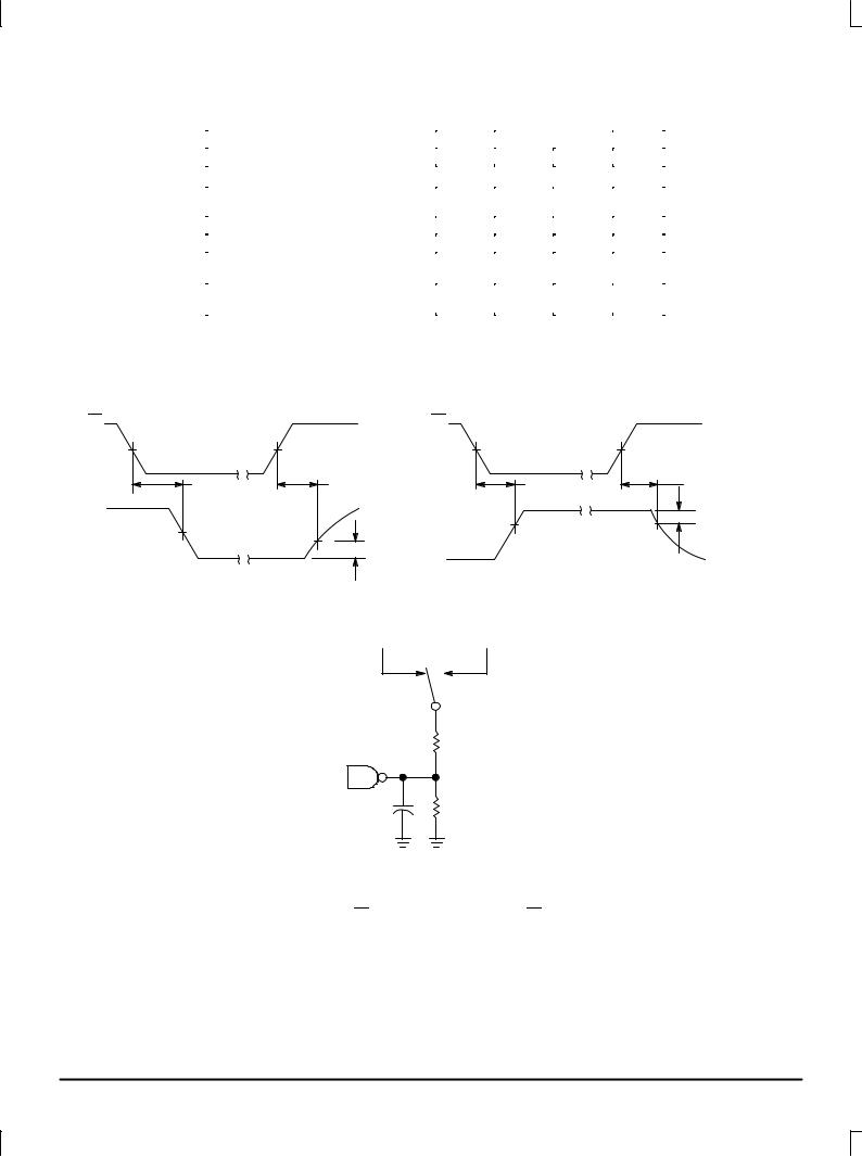
3±STATE SWITCHING WAVEFORMS
3±STATE OUTPUT LOW ENABLE AND DISABLE TIMES
3±STATE OUTPUT HIGH ENABLE AND DISABLE TIMES
OE |
|
|
OE |
|
|
1.5 V |
1.5 V |
1.5 V |
1.5 V |
|
TPZL |
TPLZ |
TPZH |
TPHZ |
VOUT |
1.5 V |
|
1.5 V |
Q VOH ≈ 3.5 V |
|
|
|||
|
VOUT |
|
||
|
|
|
||
|
|
VOL |
|
0.3 V |
|
|
|
|
|
|
|
0.3 V |
|
|
|
|
TEST LOAD |
|
|
|
|
+7.0 V |
OPEN |
|
|
|
TPZL,TPLZ,O,C, |
ALL OTHER |
|
500 Ω
D.U.T
.
50 PF |
500 Ω |
|
*INCLUDES JIG AND PROBE CAPACITANCE
Application Note: Pin 9 is an OE and the 10H350 is disabled when OE is at VIH or higher.
MOTOROLA |
2±58 |
MECL Data |
|
|
DL122 Ð Rev 6 |
 Loading...