


PIC12CE518T-04I-SM
Microchip Technology Inc PIC12CE518T-04I-SM, PIC12CE519-04-JW, PIC12CE519-04-P, PIC12CE519-04E-P, PIC12CE519-04E-SM Datasheet
...
1997 Microchip Technology Inc.
Preliminary
DS40172A-page 1
Devices:
PIC12CE518 and PIC12CE519 are 8-bit microcontrollers packaged in 8-lead packages. They are based on
the Enhanced PIC16C5X family.
High-Performance RISC CPU:
• Only 33 single word instructions to learn
• All instructions are single cycle (1 µs) except for
program branches which are two-cycle
• Operating speed: DC - 4 MHz clock input
DC - 1 µs instruction cycle
• 12-bit wide instructions
• 8-bit wide data path
• Special function hardware registers
• Two-level deep hardware stack
• Direct, indirect and relative addressing modes for
data and instructions
Peripheral Features:
• 8-bit real-time clock/counter (TMR0) with 8-bit
programmable prescaler
• 1,000,000 erase/write cycle EEPROM data
memory
• EEPROM data retention > 40 years
Device
Memory
EPROM
Program
RAM
Data
EEPROM
Data
PIC12CE518 512 x 12 25 x 8 16 x 8
PIC12CE519 1024 x 12 41 x 8 16 x 8
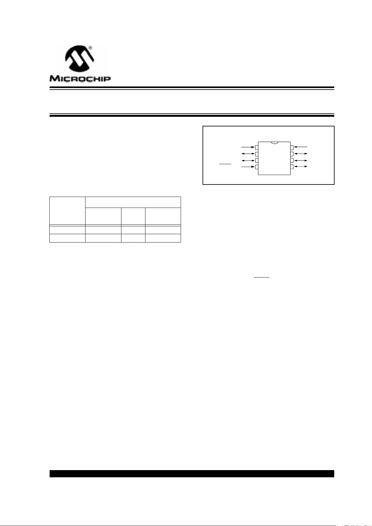
Pin Diagram:
Special Microcontroller Features:
• In-Circuit Serial Programming (ICSP™) of program memory (via two pins)
• Internal 4 MHz RC oscillator with programmable
calibration
• Power-on Reset (POR)
• Device Reset Timer (DRT)
• Watchdog Timer (WDT) with its own on-chip RC
oscillator for reliable operation
• Programmable code-protection
• Power saving SLEEP mode
• Wake-up from SLEEP on pin change
• Internal weak pull-ups on I/O pins
• Internal pull-up on MCLR
pin
• Selectable oscillator options:
- INTRC: Internal 4 MHz RC oscillator
- EXTRC: External low-cost RC oscillator
- XT: Standard crystal/resonator
- LP: Power saving, low frequency crystal
CMOS Tec hnology:
• Low-power, high-speed CMOS EPROM/
EEPROM technology
• Fully static design
• Wide temperature range:
- Commercial: 0°C to +70°C
- Industrial: -40°C to +85°C
- Extended: -40°C to +125°C
• Wide operating voltage range:
-Commercial: 3.0V to 5.5V
-Industrial: 3.0V to 5.5V
-Extended: 4.5V to 5.5V
• Low power consumption
- < 2 mA typical @ 5V, 4 MHz
- 15 µA typical @ 3V, 32 kHz
- < 1 µA typical standby current
PDIP, SOIC, Windowed CERDIP
8
7
6
5
1
2
3
4
PIC12CE518
VSS
GP0
GP1
GP2/T0CKI
PIC12CE519
GP5/OSC1/CLKIN
GP4/OSC2
GP3/MCLR
/VPP
VDD
PIC12CE5XX
8-Pin, 8-Bit CMOS Microcontroller with
EEPROM Data Memory
12CF5XX_GEBook Page 1 Tuesday, October 21, 1997 8:23 AM

PIC12CE5XX
DS40172A-page 2
Preliminary
1997 Microchip Technology Inc.
TABLE OF CONTENTS
1.0 General Description..................................................................................................................................................................... 3
2.0 PIC12CE5XX Device Varieties.................................................................................................................................................... 5
3.0 Architectural Overview ................................................................................................................................................................ 7
4.0 Memory Organization................................................................................................................................................................ 11
5.0 PIC12CE518I/O Port................................................................................................................................................................. 19
6.0 EEPROM Peripheral Operation................................................................................................................................................. 21
7.0 Timer0 Module and TMR0 Register.......................................................................................................................................... 25
8.0 Special Features of the CPU..................................................................................................................................................... 29
9.0 Instruction Set Summary........................................................................................................................................................... 41
10.0 Development Support................................................................................................................................................................ 53
11.0 Electrical Characteristics - PIC12CE5XX.................................................................................................................................. 57
12.0 DC and AC Characteristics - PIC12CE5XX .............................................................................................................................. 69
13.0 Packaging Information............................................................................................................................................................... 73
14.0 Appendix A................................................................................................................................................................................ 77
Index .................................................................................................................................................................................................... 83
PIC12CE5XX Product Identification System........................................................................................................................................ 87
To Our Valued Customers
We constantly strive to improve the quality of all our products and documentation. We have spent an exceptional
amount of time to ensure that these documents are correct. However, we realize that we may have missed a few
things. If you find any information that is missing or appears in error, please use the reader response form in the
back of this data sheet to inform us. We appreciate your assistance in making this a better document.
12CF5XX_GEBook Page 2 Tuesday, October 21, 1997 8:23 AM

1997 Microchip Technology Inc.
Preliminary
DS40172A-page 3
PIC12CE5XX
1.0 GENERAL DESCRIPTION
The 8-pin PIC12CE5XX from Microchip Technology is
a family of low-cost, high performance, 8-bit, fully static ,
EPROM/EEPROM-based CMOS microcontrollers. It
employs a RISC architecture with only 33 single word/
single cycle instructions. All instructions are single
cycle (1 µs) except for program branches which take
two cycles. The PIC12CE5XX delivers performance an
order of magnitude higher than its competitors in the
same price category. The 12-bit wide instructions are
highly symmetrical resulting in 2:1 code compression
over other 8-bit microcontrollers in its class. The easy
to use and easy to remember instruction set reduces
development time significantly.
The PIC12CE5XX products are equipped with special
features that reduce system cost and power requirements. The Power-On Reset (POR) and Device Reset
Timer (DRT) eliminate the need for external reset circuitry. There are four oscillator configurations to choose
from, including INTRC internal oscillator mode and the
power-saving LP (Low Power) oscillator. Power saving
SLEEP mode, Watchdog Timer and code protection
features improve system cost, power and reliability.
The PIC12CE5XX are available in the cost-effective
One-Time-Programmable (OTP) versions which are
suitable for production in any volume. The customer
can take full advantage of Microchip’s price leadership
in OTP microcontrollers while benefiting from the O TP’s
flexibility .
The PIC12CE5XX products are supported by a full-featured macro assembler, a software simulator, an in-circuit emulator, a ‘C’ compiler, fuzzy logic support tools,
a low-cost development programmer, and a full featured programmer. All the tools are supported on IBM
PC and compatible machines.
1.1 Applications
The PIC12CE5XX series fits perfectly in applications
ranging from sensory systems, gas detectors and
security systems to low-power remote transmitters/
receivers. The EPROM programming technology
makes customizing application programs (transmitter
codes, appliance settings, receiver frequencies, etc.)
extremely fast and convenient. While the EEPROM
data memory technology allows for the changing of calibrations factors and security codes, the small footprint
8-pin packages, for through hole or surface mounting,
make this microcontroller series perfect for applications
with space limitations. Low-cost, low-power, high performance, ease of use and I/O flexibility make the
PIC12CE5XX series very versatile even in areas where
no microcontroller use has been considered before
(e.g., timer functions, replacement of “glue” logic and
PLD’s in larger systems, coprocessor applications).
12CF5XX_GEBook Page 3 Tuesday, October 21, 1997 8:23 AM

PIC12CE5XX
DS40172A-page 4
Preliminary
1997 Microchip Technology Inc.
TABLE 1-1: PIC12CXXX FAMILY OF DEVICES
PIC12C508(A)
PIC12C509(A) PIC12CE518 PIC12CE519 PIC12C671 PIC12C672
Clock
Maximum Frequency
of Operation (MHz)
4 4 4 4 10 10
Memory
EPROM Program
Memory
512 x 12 1024 x 12 512 x 12 1024 x 12 1024 x 14 2048 x 14
RAM Data Memory
(bytes)
25 41 25 41 128 128
Peripherals
EEPROM Data Memory (bytes)
16 16
Timer Module(s) TMR0 TMR0 TMR0 TMR0 TMR0 TMR0
A/D Converter (8-bit)
Channels
— — — — 4 4
Features
Wake-up from
SLEEP on
pin change
Yes Yes Yes Yes Yes Yes
Interrupt Sources — — 4 4
I/O Pins 5 5 5 5 5 5
Input Pins 1 1 1 1 1 1
Internal Pull-ups Yes Yes Yes Yes Yes Yes
In-Circuit Serial Pro-
gramming
Yes Yes Yes Yes Yes Yes
Number of Instructions
33 33 33 33 35 35
Packages 8-pin DIP,
JW, SOIC
8-pin DIP,
JW, SOIC
8-pin DIP,
JW, SOIC
8-pin DIP,
JW, SOIC
8-pin DIP,
JW, SOIC
8-pin DIP,
JW, SOIC
All PIC12CE5XX devices have Power-on Reset, selectable Watchdog Timer, selectable code protect and high I/O current capability.
All PIC12CE5XX devices use serial programming with data pin GP0 and clock pin GP1.
12CF5XX_GEBook Page 4 Tuesday, October 21, 1997 8:23 AM

1997 Microchip Technology Inc.
Preliminary
DS40172A-page 5
PIC12CE5XX
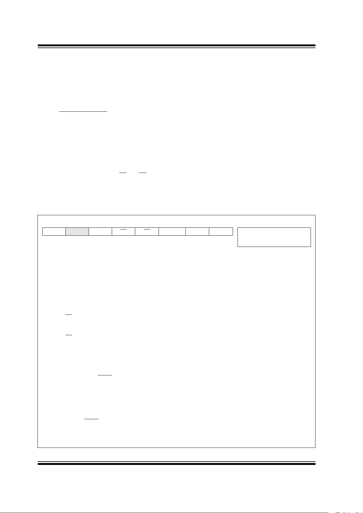
2.0 PIC12CE5XX DEVICE
VARIETIES
A variety of packaging options are available.
Depending on application and production
requirements, the proper device option can be
selected using the information in this section. When
placing orders, please use the PIC12CE5XX Product
Identification System at the back of this data sheet to
specify the correct part number.
2.1 UV Erasab
le Devices
The UV erasable version, offered in windowed cerdip
package, is optimal for prototype development and
pilot programs.
The UV erasable version can be erased and
reprogrammed to any of the configuration modes.
Microchip's PICST ART
PLUS and PRO MATE programmers all support programming of the
PIC12CE5XX. Third party programmers also are available; refer to the
Microchip Third Party Guide
for a list
of sources.
2.2 O
ne-Time-Programmable (OTP)
Devices
The availability of OTP devices is especially useful for
customers who need the flexibility for frequent code
updates or small volume applications.
The OTP devices , packaged in plastic pac kages permit
the user to program them once. In addition to the
program memory, the configuration bits must also be
programmed.
Note:
Please note that erasing the device will
also erase the pre-programmed internal
calibration value for the inter nal oscillator.
The calibration value must be saved prior
to erasing the part.
2.3 Quic
k-Turnaround-Production (QTP)
Devices
Microchip offers a QTP Programming Service for
factory production orders. This service is made
available for users who choose not to program a
medium to high quantity of units and whose code
patterns have stabilized. The devices are identical to
the OTP devices b ut with all EPROM locations and fuse
options already programmed by the factory. Certain
code and prototype verification procedures do apply
before production shipments are availab le. Please contact your local Microchip Technology sales office for
more details.
2.4 Serializ
ed Quick-Turnaround
Production (SQTP
SM
) De
vices
Microchip offers a unique programming service where
a few user-defined locations in each device are
programmed with different serial numbers. The serial
numbers may be random, pseudo-random or
sequential.
Serial programming allows each device to have a
unique number which can serve as an entry-code,
password or ID number.
12CF5XX_GEBook Page 5 Tuesday, October 21, 1997 8:23 AM

PIC12CE5XX
DS40172A-page 6
Preliminary
1997 Microchip Technology Inc.
NOTES:
12CF5XX_GEBook Page 6 Tuesday, October 21, 1997 8:23 AM

1997 Microchip Technology Inc.
Preliminary
DS40172A-page 7
PIC12CE5XX
3.0 ARCHITECTURAL OVERVIEW
The high performance of the PIC12CE5XX family can
be attributed to a number of architectural features
commonly found in RISC microprocessors. To begin
with, the PIC12CE5XX uses a Harvard architecture in
which program and data are accessed on separate
buses. This improves bandwidth over traditional von
Neumann architecture where program and data are
fetched on the same bus. Separating program and
data memory further allows instructions to be sized
differently than the 8-bit wide data word. Instruction
opcodes are 12-bits wide making it possible to have all
single word instructions. A 12-bit wide program
memory access bus fetches a 12-bit instruction in a
single cycle. A two-stage pipeline overlaps fetch and
execution of instructions. Consequently, all instructions
(33) execute in a single cycle (1µs @ 4MHz) except for
program branches.
The PIC12CE518 addresses 512 x 12 of program
memory, the PIC12CE519 addresses 1K x 12 of
program memory. All program memory is internal.
The PIC12CE5XX can directly or indirectly address its
register files and data memory. All special function
registers including the program counter are mapped in
the data memory. The PIC12CE5XX has a highly
orthogonal (symmetrical) instruction set that makes it
possible to carry out any operation on any register
using any addressing mode. This symmetrical nature
and lack of ‘special optimal situations’ make
programming with the PIC12CE5XX simple yet
efficient. In addition, the learning curve is reduced
significantly.
The PIC12CE5XX contains a 16 X 8 EEPROM
memory array for storing non-volatile information such
as calibration data or security codes. This memory
has an endurance of 1,000,000 erase/write cycles and
a retention of 40+ years.
The PIC12CE5XX device contains an 8-bit ALU and
working register. The ALU is a general purpose
arithmetic unit. It performs arithmetic and Boolean
functions between data in the working register and any
register file.
The ALU is 8-bits wide and capable of addition,
subtraction, shift and logical operations. Unless
otherwise mentioned, arithmetic operations are two's
complement in nature. In two-operand instructions,
typically one operand is the W (working) register. The
other operand is either a file register or an immediate
constant. In single operand instructions, the operand
is either the W register or a file register.
The W register is an 8-bit working register used for
ALU operations. It is not an addressable register.
Depending on the instruction executed, the ALU may
affect the values of the Carry (C), Digit Carry (DC),
and Zero (Z) bits in the STATUS register. The C and
DC bits operate as a borr
ow and digit borrow out bit,
respectively, in subtraction. See the
SUBWF
and
ADDWF
instructions for examples.
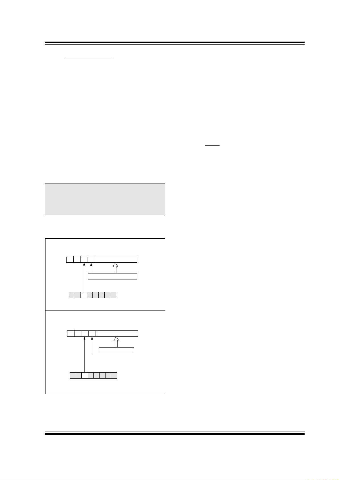
A simplified block diagram is shown in Figure 3-1, with
the corresponding device pins described in Table 3-1.
12CF5XX_GEBook Page 7 Tuesday, October 21, 1997 8:23 AM

PIC12CE5XX
DS40172A-page 8
Preliminary
1997 Microchip Technology Inc.
FIGURE 3-1: PIC12CE5XX BLOCK DIAGRAM
Device Reset
Timer
Power-on
Reset
Watchdog
Timer
EPROM
Program
Memory
12
Data Bus
8
12
Program
Bus
Instruction reg
Program Counter
RAM
File
Registers
Direct Addr
5
RAM Addr
9
Addr MUX
Indirect
Addr
FSR reg
STATUS reg
MUX
ALU
W reg
Instruction
Decode &
Control
Timing
Generation
OSC1/CLKIN
OSC2
MCLR
V
DD, VSS
Timer0
GPIO
8
8
GP4/OSC2
GP3/MCLR/VPP
GP2/T0CKI
GP1
GP0
5-7
3
GP5/OSC1/CLKIN
STACK1
STACK2
512 x 12 or
25 x 8 or
1024 x 12
41 x 8
Internal RC
OSC
16 X 8
EEPROM
Data
Memory
SCL
SDA
12CF5XX_GEBook Page 8 Tuesday, October 21, 1997 8:23 AM

1997 Microchip Technology Inc.
Preliminary
DS40172A-page 9
PIC12CE5XX
TABLE 3-1: PIC12CE5XX PINOUT DESCRIPTION
Name
DIP
Pin #
SOIC
Pin #
I/O/P
Type
Buffer
Type
Description
GP0 7 7 I/O TTL/ST Bi-directional I/O port/ serial programming data. Can
be software programmed for internal weak pull-up and
wake-up from SLEEP on pin change. This buffer is a
Schmitt Trigger input when used in serial programming
mode.
GP1 6 6 I/O TTL/ST Bi-directional I/O port/ serial programming clock. Can
be software programmed for internal weak pull-up and
wake-up from SLEEP on pin change. This buffer is a
Schmitt Trigger input when used in serial programming
mode.
GP2/T0CKI 5 5 I/O ST Bi-directional I/O port. Can be configured as T0CKI.
GP3/MCLR
/V
PP
4 4 I TTL Input port/master clear (reset) input/programming volt-
age input. When configured as MCLR
, this pin is an
active low reset to the device. Voltage on MCLR
/VPP
must not exceed VDD during normal device operation.
Can be software programmed for internal weak pull-up
and wake-up from SLEEP on pin change. Weak pullup always on if configured as MCLR
GP4/OSC2 3 3 I/O TTL Bi-directional I/O port/oscillator crystal output. Con-
nections to crystal or resonator in crystal oscillator
mode (XT and LP modes only, GPIO in other modes).
GP5/OSC1/CLKIN 2 2 I/O TTL/ST Bidirectional IO port/oscillator crystal input/external
clock source input (GPIO in Internal RC mode only,
OSC1 in all other oscillator modes). TTL input when
GPIO, ST input in external RC oscillator mode.
V
DD
1 1 P — Positive supply for logic and I/O pins
V
SS
8 8 P — Ground reference for logic and I/O pins
Legend: I = input, O = output, I/O = input/output, P = power, — = not used, TTL = TTL input,
ST = Schmitt Trigger input
12CF5XX_GEBook Page 9 Tuesday, October 21, 1997 8:23 AM
PIC12CE5XX
DS40172A-page 10
Preliminary
1997 Microchip Technology Inc.
3.1 Cloc
king Scheme/Instruction Cycle
The clock input (OSC1/CLKIN pin) is internally divided
by four to generate four non-overlapping quadrature
clocks namely Q1, Q2, Q3 and Q4. Internally, the
program counter is incremented every Q1, and the
instruction is fetched from program memory and
latched into instruction register in Q4. It is decoded
and executed during the following Q1 through Q4. The
clocks and instruction execution flow is shown in
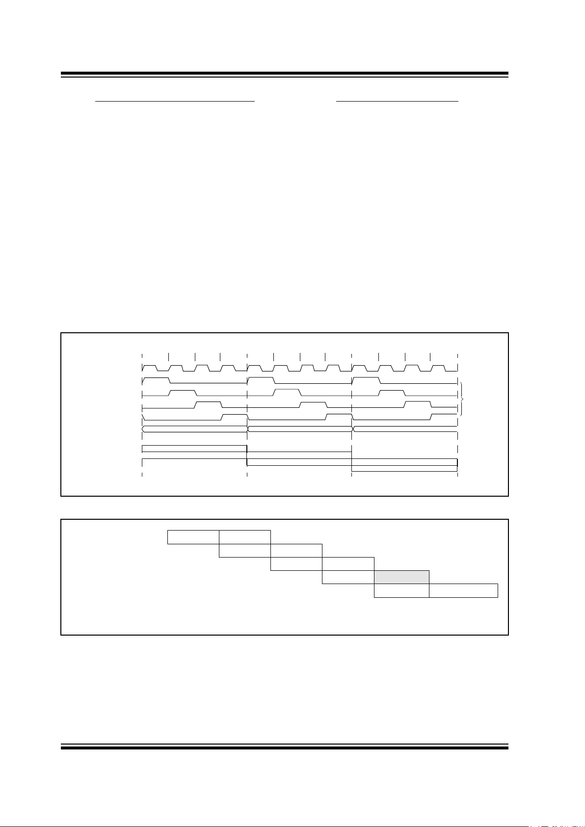
Figure 3-2 and Example 3-1.
3.2 Instruction Flo
w/Pipelining
An Instruction Cycle consists of four Q cycles (Q1, Q2,
Q3 and Q4). The instruction fetch and execute are
pipelined such that fetch takes one instruction cycle
while decode and execute takes another instruction
cycle. However, due to the pipelining, each instruction
effectively executes in one cycle. If an instruction
causes the program counter to change (e.g.,
GOTO
)
then two cycles are required to complete the
instruction (Example 3-1).
A fetch cycle begins with the program counter (PC)
incrementing in Q1.
In the execution cycle, the fetched instruction is
latched into the Instruction Register (IR) in cycle Q1.
This instruction is then decoded and executed during
the Q2, Q3, and Q4 cycles. Data memory is read
during Q2 (operand read) and written during Q4
(destination write).
FIGURE 3-2: CLOCK/INSTRUCTION CYCLE
EXAMPLE 3-1: INSTRUCTION PIPELINE FLOW
Q1
Q2 Q3 Q4
Q1
Q2 Q3 Q4
Q1
Q2 Q3 Q4
OSC1
Q1
Q2
Q3
Q4
PC
PC PC+1 PC+2
Fetch INST (PC)
Execute INST (PC-1) Fetch INST (PC+1)
Execute INST (PC) Fetch INST (PC+2)
Execute INST (PC+1)
Internal
phase
clock
All instructions are single cycle, except for any program branches. These take two cycles since the fetch
instruction is “flushed” from the pipeline while the new instruction is being fetched and then executed.
1. MOVLW 03H
Fetch 1 Execute 1
2. MOVWF GPIO
Fetch 2 Execute 2
3. CALL SUB_1
Fetch 3 Execute 3
4. BSF GPIO, BIT1
Fetch 4 Flush
Fetch SUB_1 Execute SUB_1
12CF5XX_GEBook Page 10 Tuesday, October 21, 1997 8:23 AM
1997 Microchip Technology Inc.
Preliminary
DS40172A-page 11
PIC12CE5XX
4.0 MEMORY ORGANIZATION
PIC12CE5XX memory is organized into program memory and data memory. For devices with more than 512
bytes of program memory, a paging scheme is used.
Program memory pages are accessed using one STATUS register bit. For the PIC12CE519 with a data
memory register file of more than 32 registers, a banking scheme is used. Data memory banks are accessed
using the File Select Register (FSR).
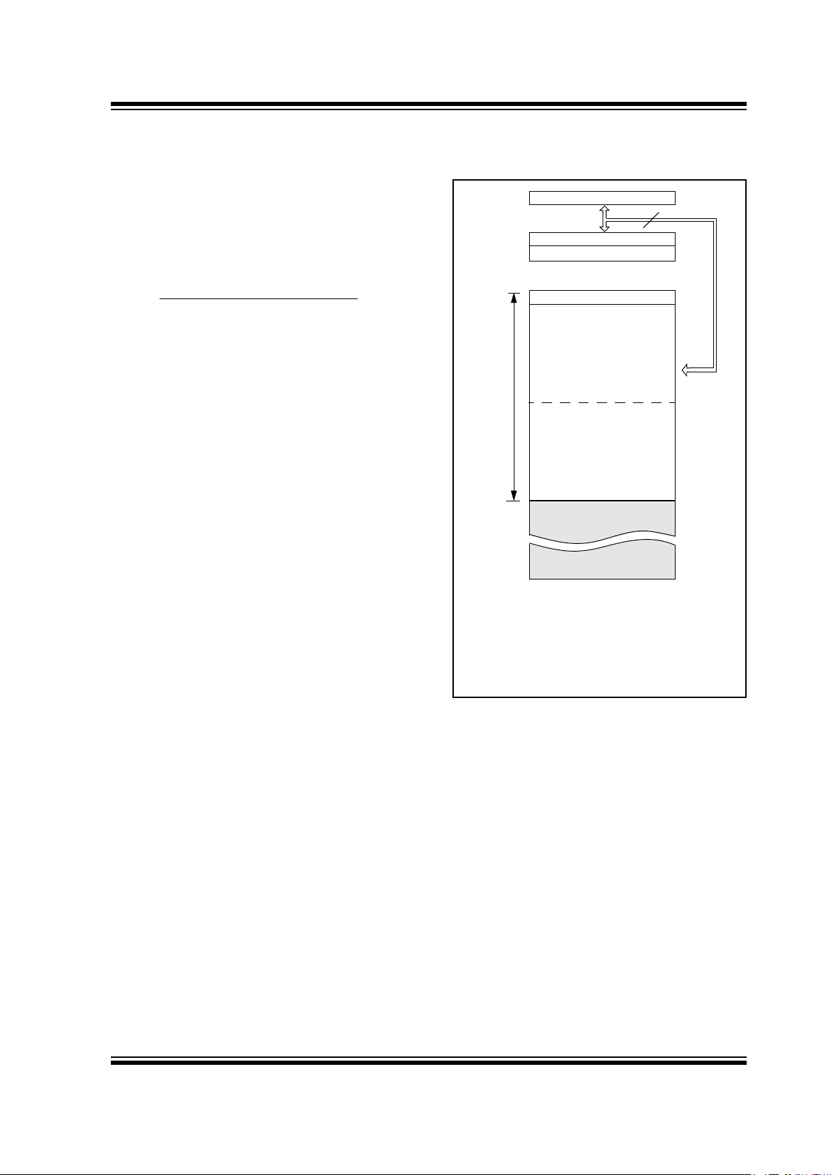
4.1 Pr
ogram Memory Organization
The PIC12CE5XX devices have a 12-bit Program
Counter (PC) capable of addressing a 2K x 12
program memory space.
Only the first 512 x 12 (0000h-01FFh) for the
PIC12CE518 and 1K x 12 (0000h-03FFh) for the
PIC12CE519 are physically implemented. Refer to
Figure 4-1. Accessing a location above these
boundaries will cause a wrap-around within the first
512 x 12 space (PIC12CE518) or 1K x 12 space
(PIC12CE519). The effective reset vector is at 000h,
(see Figure 4-1). Location 01FFh (PIC12CE518) or
location 03FFh (PIC12CE519), the hardwired reset
vector location, contains the internal clock oscillator
calibration value. This value is set at Microchip and
should never be overwritten. Upon reset, the
MOVLW XX is executed, the PC wraps to location
0000h, thus making 0000h the effective reset vector.
FIGURE 4-1: PROGRAM MEMORY MAP
AND STACK FOR THE
PIC12CE5XX
CALL, RETLW
PC<11:0>
Stack Level 1
Stack Level 2
User Memory
Space
12
0000h
7FFh
01FFh
0200h
On-chip Program
Memory
Reset Vector (note 1)
Note 1: Address 0000h becomes the
effective reset vector. Location
01FFh (PIC12CE518) or location
03FFh (PIC12CE519) contains the
MOVLW XX INTRC oscillator
calibration value.
512 Word (PIC12CE518)
1024 Word (PIC12CE519)
03FFh
0400h
On-chip Program
Memory
12CF5XX_GEBook Page 11 Tuesday, October 21, 1997 8:23 AM
PIC12CE5XX
DS40172A-page 12
Preliminary
1997 Microchip Technology Inc.
4.2 Data Memor
y Organization
Data memory is composed of registers, or bytes of
RAM. Therefore, data memory for a device is specified
by its register file. The register file is divided into two
functional groups: special function registers and
general purpose registers.
The special function registers include the TMR0
register, the Program Counter (PC), the Status
Register, the I/O registers (ports), and the File Select
Register (FSR). In addition, special purpose registers
are used to control the I/O port configuration and
prescaler options.
The general purpose registers are used for data and
control information under command of the instructions.
For the PIC12CE518, the register file is composed of 7
special function registers and 25 general purpose
registers (Figure 4-2).
For the PIC12CE519, the register file is composed of 7
special function registers, 25 general purpose
registers, and 16 general purpose registers that may
be addressed using a banking scheme (Figure 4-3).
4.2.1 GENERAL PURPOSE REGISTER FILE
The general purpose register file is accessed either
directly or indirectly through the file select register
FSR (Section 4.8).
FIGURE 4-2: PIC12CE518 REGISTER FILE
MAP
File Address
00h
01h
02h
03h
04h
05h
06h
07h
1Fh
INDF
(1)
TMR0
PCL
STATUS
FSR
OSCCAL
GPIO
General
Purpose
Registers
Note 1: Not a physical register. See Indirect
Data Addressing, Section 4.8.
FIGURE 4-3: PIC12CE519 REGISTER FILE MAP
File Address
00h
01h
02h
03h
04h
05h
06h
07h
1Fh
INDF
(1)
TMR0
PCL
STATUS
FSR
OSCCAL
GPIO
0Fh
10h
Bank 0 Bank 1
3Fh
30h
20h
2Fh
General
Purpose
Registers
General
Purpose
Registers
General
Purpose
Registers
Addresses map
back to
addresses
in Bank 0.
Note 1: Not a physical register. See Indirect
Data Addressing, Section 4.8.
FSR<6:5> 00 01
12CF5XX_GEBook Page 12 Tuesday, October 21, 1997 8:23 AM
1997 Microchip Technology Inc.
Preliminary
DS40172A-page 13
PIC12CE5XX
4.2.2 SPECIAL FUNCTION REGISTERS
The Special Function Registers (SFRs) are registers
used by the CPU and peripheral functions to control
the operation of the device (Table 4-1).
The special registers can be classified into two sets.
The special function registers associated with the
“core” functions are described in this section. Those
related to the operation of the peripheral features are
described in the section for each peripheral feature.
TABLE 4-1: SPECIAL FUNCTION REGISTER (SFR) SUMMARY
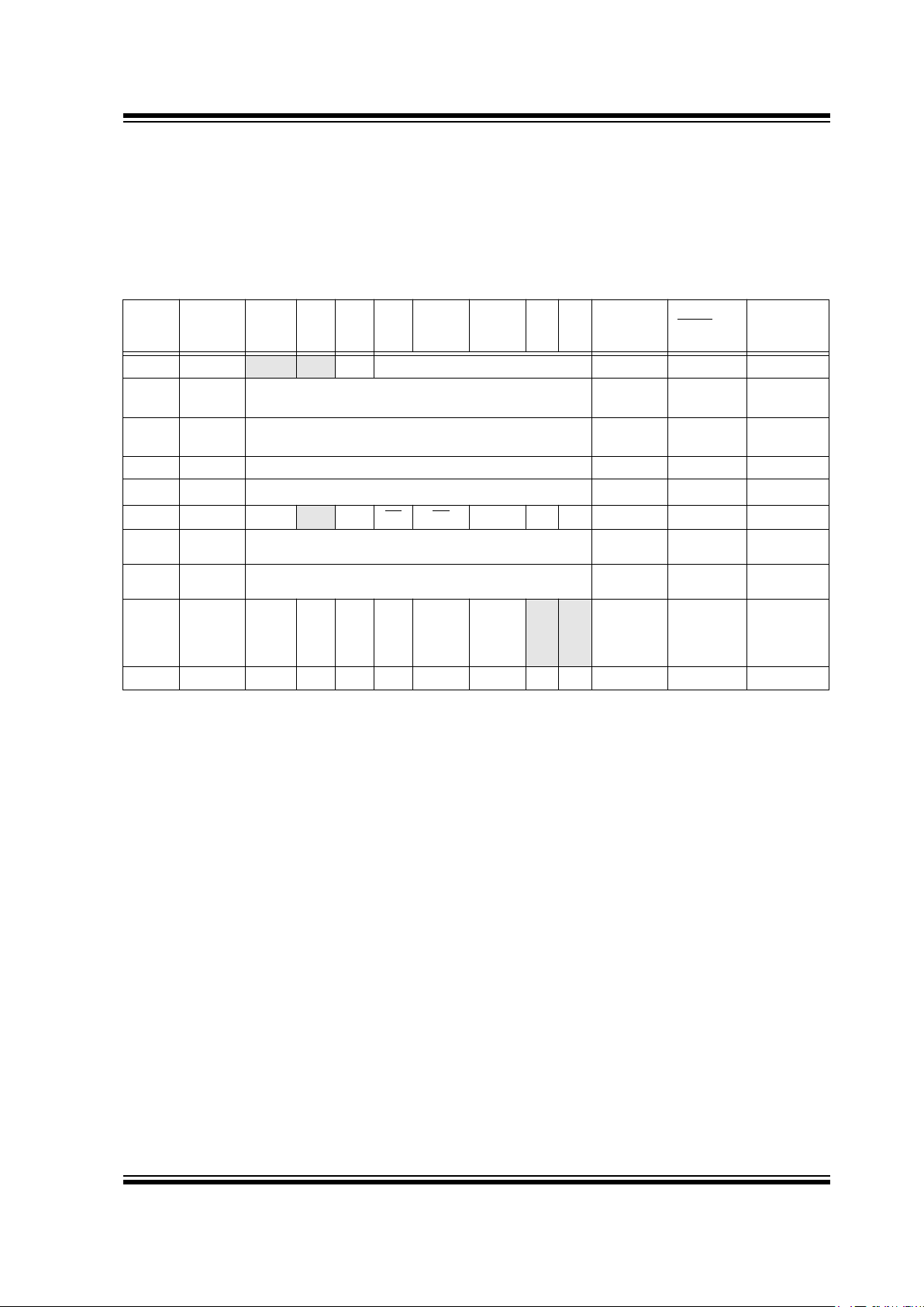
Address Name Bit 7 Bit 6 Bit 5 Bit 4 Bit 3 Bit 2 Bit 1 Bit 0
Value on
Power-On
Reset
Value on
M
CLR and
WDT Reset
Value on
Wake-up on
Pin Change
N/A TRIS
—
—
I/O control registers
--11 1111 --11 1111 --11 1111
N/A OPTION
Contains control bits to configure Timer0, Timer0/WDT
prescaler, wake-up on change, and weak pull-ups
1111 1111 1111 1111 1111 1111
00h INDF
Uses contents of FSR to address data memory (not a physical
register)
xxxx xxxx uuuu uuuu uuuu uuuu
01h TMR0 8-bit real-time clock/counter
xxxx xxxx uuuu uuuu uuuu uuuu
02h
(1)
PCL Low order 8 bits of PC
1111 1111 1111 1111 1111 1111
03h STATUS GPWUF
—
PA0 T
O PD Z DC C
0001 1xxx 000q quuu 100q quuu
04h
FSR
(12CE518)
Indirect data memory address pointer
111x xxxx 111u uuuu 111u uuuu
04h
FSR
(12CE519)
Indirect data memory address pointer
110x xxxx 11uu uuuu 11uu uuuu
05h
OSCCAL
(12CE518/
12CE519)
CAL7 CAL6 CAL5 CAL4 CALFST CALSLW — —
0111 00-- uuuu uu-- uuuu uu--
06h GPIO SCL SDA GP5 GP4 GP3 GP2 GP1 GP0 11xx xxxx 11uu uuuu 11uu uuuu
Legend: Shaded boxes = unimplemented or unused, — = unimplemented, read as '0' (if applicable)
x = unknown, u = unchanged, q = see the tables in Section 8.7 for possible values.
Note 1: The upper byte of the Program Counter is not directly accessible. See Section 4.6
for an explanation of how to access these bits.
12CF5XX_GEBook Page 13 Tuesday, October 21, 1997 8:23 AM
PIC12CE5XX
DS40172A-page 14 Preliminary 1997 Microchip Technology Inc.
4.2.3 EEPROM DATA MEMORY
The PIC12CE518 and PIC12CE519 each have 16
bytes of EEPROM data memory. The EEPROM data
memory supports a bi-directional 2-wire bus and data
transmission protocol. Refer to Section 6.0 on
EEPROM Peripherals.
4.3 STATUS Register
This register contains the arithmetic status of the ALU,
the RESET status, and the page preselect bit for
program memories larger than 512 words.
The STATUS register can be the destination for any
instruction, as with any other register. If the STATUS
register is the destination for an instruction that affects
the Z, DC or C bits, then the write to these three bits is
disabled. These bits are set or cleared according to
the device logic. Further more, the T
O and PD bits are
not writable. Therefore, the result of an instruction with
the STATUS register as destination may be different
than intended.
For example, CLRF STATUS will clear the upper three
bits and set the Z bit. This leaves the STATUS register
as 000u u1uu (where u = unchanged).
It is recommended, therefore, that only BCF, BSF and
MOVWF instructions be used to alter the STATUS
register because these instructions do not affect the Z,
DC or C bits from the STATUS register. For other
instructions, which do affect STATUS bits, see
Instruction Set Summary.
FIGURE 4-4: STATUS REGISTER (ADDRESS:03h)
R/W-0 R/W-0 R/W-0 R-1 R-1 R/W-x R/W-x R/W-x
GPWUF
—
PA0 TO PD Z DC C R = Readable bit
W = Writable bit
- n = Value at POR reset
bit7 6 5 4 3 2 1 bit0
bit 7: GPWUF: GPIO reset bit
1 = Reset due to wake-up from SLEEP on pin change
0 = After power up or other reset
bit 6: Unimplemented
bit 5: PA0: Program page preselect bits
1 = Page 1 (200h - 3FFh) - PIC12CE519
0 = Page 0 (000h - 1FFh) - PIC12CE518 and PIC12CE519
Each page is 512 bytes.
Using the PA0 bit as a general purpose read/write bit in devices which do not use it for program
page preselect is not recommended since this may affect upward compatibility with future products.
bit 4: TO: Time-out bit
1 = After power-up, CLRWDT instruction, or SLEEP instruction
0 = A WDT time-out occurred
bit 3: PD: Power-down bit
1 = After power-up or by the CLRWDT instruction
0 = By execution of the SLEEP instruction
bit 2: Z: Zero bit
1 = The result of an arithmetic or logic operation is zero
0 = The result of an arithmetic or logic operation is not zero
bit 1: DC: Digit carry/borrow bit (for ADDWF and SUBWF instructions)
ADDWF
1 = A carry from the 4th low order bit of the result occurred
0 = A carry from the 4th low order bit of the result did not occur
SUBWF
1 = A borrow from the 4th low order bit of the result did not occur
0 = A borrow from the 4th low order bit of the result occurred
bit 0: C: Carry/borrow bit (for ADDWF, SUBWF and RRF, RLF instructions)
ADDWF SUBWF RRF or RLF
1 = A carry occurred 1 = A borrow did not occur Load bit with LSB or MSB, respectively
0 = A carry did not occur 0 = A borrow occurred
12CF5XX_GEBook Page 14 Tuesday, October 21, 1997 8:23 AM

1997 Microchip Technology Inc. Preliminary DS40172A-page 15
PIC12CE5XX
4.4 OPTION Register
The OPTION register is a 8-bit wide, write-only
register which contains various control bits to
configure the Timer0/WDT prescaler and Timer0.
By executing the OPTION instruction, the contents of
the W register will be transferred to the OPTION
register. A RESET sets the OPTION<7:0> bits.
Note: If TRIS bit is set to ‘0’, the wake-up on
change and pull-up functions are disabled
for that pin; i.e., note that TRIS overrides
OPTION control of GPPU
and GPWU.
Note: If the T0CS bit is set to ‘1’, GP2 is f orced to
be an input even if TRIS GP2 = ‘0’.
FIGURE 4-5: OPTION REGISTER
W-1 W-1 W-1 W-1 W-1 W-1 W-1 W-1
GPWU GPPU T0CS T0SE PSA PS2 PS1 PS0 W = Writable bit
U = Unimplemented bit
- n = Value at POR reset
Reference Table 4-1 for
other resets.
bit7 6 5 4 3 2 1 bit0
bit 7: GPWU: Enable wake-up on pin change (GP0, GP1, GP3)
1 = Disabled
0 = Enabled
bit 6: GPPU: Enable weak pull-ups (GP0, GP1, GP3)
1 = Disabled
0 = Enabled
bit 5: T0CS: Timer0 clock source select bit
1 = Transition on T0CKI pin
0 = Transition on internal instruction cycle clock, Fosc/4
bit 4: T0SE: Timer0 source edge select bit
1 = Increment on high to low transition on the T0CKI pin
0 = Increment on low to high transition on the T0CKI pin
bit 3: PSA: Prescaler assignment bit
1 = Prescaler assigned to the WDT
0 = Prescaler assigned to Timer0
bit 2-0: PS2:PS0: Prescaler rate select bits
000
001
010
011
100
101
110
111
1 : 2
1 : 4
1 : 8
1 : 16
1 : 32
1 : 64
1 : 128
1 : 256
1 : 1
1 : 2
1 : 4
1 : 8
1 : 16
1 : 32
1 : 64
1 : 128
Bit Value Timer0 Rate WDT Rate
12CF5XX_GEBook Page 15 Tuesday, October 21, 1997 8:23 AM

PIC12CE5XX
DS40172A-page 16 Preliminary 1997 Microchip Technology Inc.
4.5 OSCCAL Register
The Oscillator Calibration (OSCCAL) register is used to
calibrate the internal 4 MHz oscillator. It contains four
bits for fine calibration and two other bits to either
increase or decrease frequency.
FIGURE 4-6: OSCCAL REGISTER (ADDRESS 8Fh)
R/W-0 R/W-1 R/W-1 R/W-1 R/W-0 R/W-0 U-0 U-0
CAL3 CAL2 CAL1 CAL0 CALFST CALSLW — — R = Readable bit
W = Writable bit
U = Unimplemented bit,
read as ‘0’
- n = Value at POR reset
bit7 bit0
bit 7-4: CAL<3:0>: Fine calibration
bit 3: CALFST: Calibration Fast
1 = Increase frequency
0 = No change
bit 2: CALSLW: Calibration Slow
1 = Decrease frequency
0 = No change
bit 1-0: Unimplemented: Read as '0'
Note: If CALFST = 1 and CALSLW = 1, CALFST has precedence.
12CF5XX_GEBook Page 16 Tuesday, October 21, 1997 8:23 AM
1997 Microchip Technology Inc. Preliminary DS40172A-page 17
PIC12CE5XX
4.6 Program Counter
As a program instruction is executed, the Program
Counter (PC) will contain the address of the next
program instruction to be executed. The PC value is
increased by one every instruction cycle, unless an
instruction changes the PC.
For a GOTO instruction, bits 8:0 of the PC are provided
by the GOTO instruction word. The PC Latch (PCL) is
mapped to PC<7:0>. Bit 5 of the STATUS register
provides page information to bit 9 of the PC (Figure 4-
7).
For a CALL instruction, or any instruction where the
PCL is the destination, bits 7:0 of the PC again are
provided by the instruction word. However, PC<8>
does not come from the instruction word, but is always
cleared (Figure 4-7).
Instructions where the PCL is the destination, or
Modify PCL instructions, include MOVWF PC, ADDWF
PC, and BSF PC,5.
FIGURE 4-7: LOADING OF PC
BRANCH INSTRUCTIONS PIC12CE518/CE519
Note: Because PC<8> is cleared in the CALL
instruction, or any Modify PCL instruction,
all subroutine calls or computed jumps are
limited to the first 256 locations of any program memory page (512 words long).
PA0
STATUS
PC
8 7 0
PCL
910
Instruction Word
7 0
GOTO Instruction
CALL or Modify PCL Instruction
11
PA0
STATUS
PC
8 7 0
PCL
910
Instruction Word
7 0
11
Reset to ‘0’
4.6.1 EFFECTS OF RESET
The Program Counter is set upon a RESET, which
means that the PC addresses the last location in the
last page i.e., the oscillator calibration instruction. After
executing MOVLW XX, the PC will roll over to location
00h, and begin executing user code.
The STATUS register page preselect bits are cleared
upon a RESET, which means that page 0 is preselected.
Therefore, upon a RESET, a GOTO instruction will
automatically cause the program to jump to page 0
until the value of the page bits is altered.
4.7 Stack
PIC12CE5XX devices have a 12-bit wide hardware
push/pop stack.
A CALL instruction will
push
the current value of stack
1 into stack 2 and then push the current program
counter value, incremented by one , into stac k le v el 1. If
more than two sequential CALL’s are executed, only
the most recent two return addresses are stored.
A RETLW instruction will
pop
the contents of stack level
1 into the program counter and then copy stack level 2
contents into level 1. If more than two sequential
RETLW’s are executed, the stack will be filled with the
address previously stored in level 2. Note that the
W register will be loaded with the literal value specified
in the instruction. This is particularly useful for the
implementation of data look-up tables within the
program memory.
12CF5XX_GEBook Page 17 Tuesday, October 21, 1997 8:23 AM
PIC12CE5XX
DS40172A-page 18 Preliminary 1997 Microchip Technology Inc.
4.8 Indirect Data Addressing; INDF and
FSR Registers
The INDF register is not a physical register.
Addressing INDF actually addresses the register
whose address is contained in the FSR register (FSR
is a
pointer
). This is indirect addressing.
EXAMPLE 4-1: INDIRECT ADDRESSING
• Register file 07 contains the value 10h
• Register file 08 contains the value 0Ah
• Load the value 07 into the FSR register
• A read of the INDF register will return the value
of 10h
• Increment the value of the FSR register by one
(FSR = 08)
• A read of the INDR register now will return the
value of 0Ah.
Reading INDF itself indirectly (FSR = 0) will produce
00h. Writing to the INDF register indirectly results in a
no-operation (although STATUS bits may be affected).
A simple program to clear RAM locations 10h-1Fh
using indirect addressing is shown in Example 4-2.
EXAMPLE 4-2: HOW TO CLEAR RAM
USING INDIRECT
ADDRESSING
movlw 0x10 ;initialize pointer
movwf FSR ; to RAM
NEXT clrf INDF ;clear INDF register
incf FSR,F ;inc pointer
btfsc FSR,4 ;all done?
goto NEXT ;NO, clear next
CONTINUE
: ;YES, continue
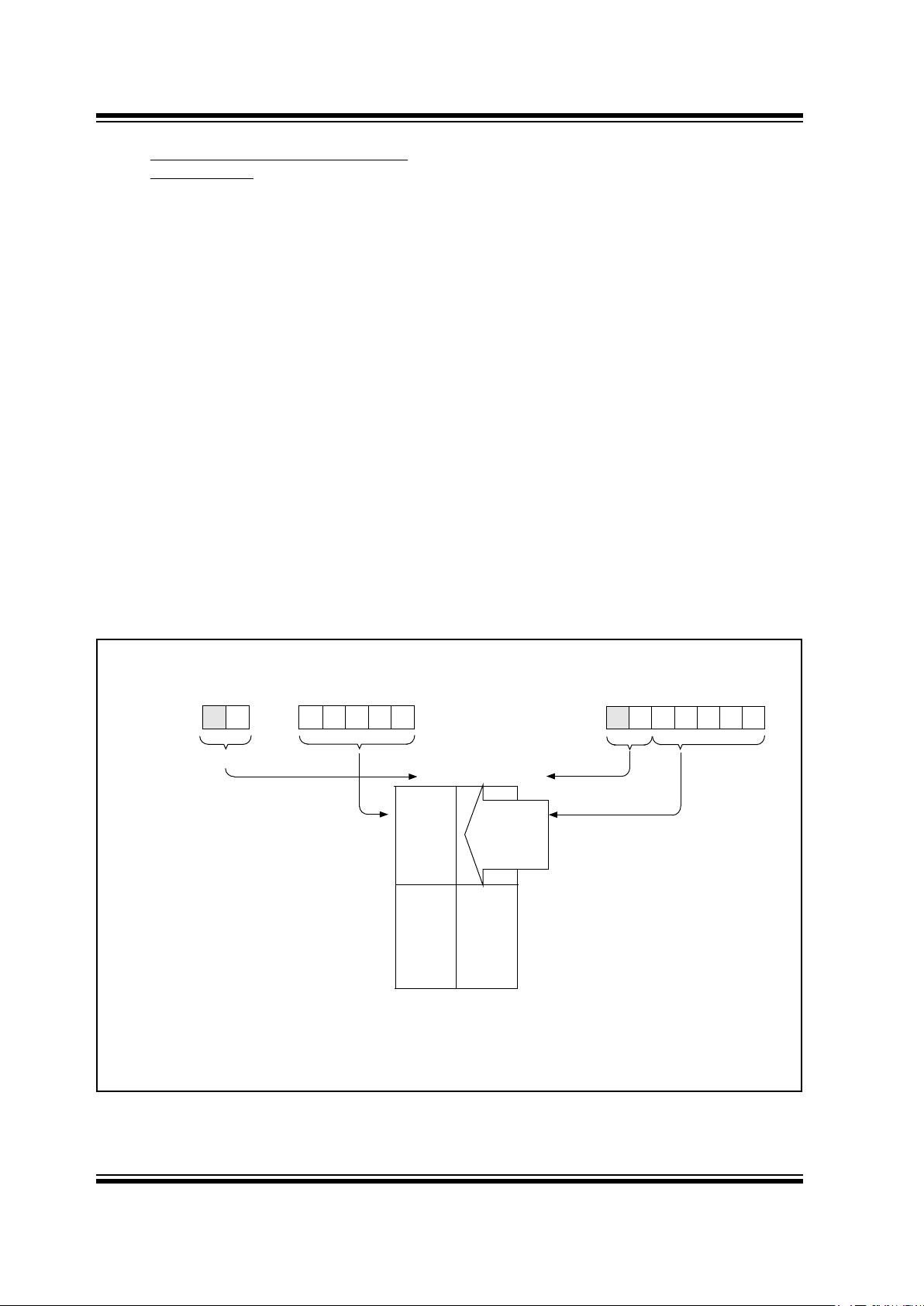
The FSR is a 5-bit wide register. It is used in
conjunction with the INDF register to indirectly address
the data memory area.
The FSR<4:0> bits are used to select data memory
addresses 00h to 1Fh.
PIC12CE518: Does not use banking. FSR<6:5> are
unimplemented and read as '1's.
PIC12CE519: Uses FSR<5>. Selects between bank 0
and bank 1. FSR<6> is unimplemented, read as '1’ .
FIGURE 4-8: DIRECT/INDIRECT ADDRESSING
Note 1: For register map detail see Section 4.2.
Note 2: PIC12CE519 only
bank
location select
location select
bank select
Indirect Addressing
Direct Addressing
Data
Memory
(1)
0Fh
10h
Bank 0 Bank 1
(2)
0
4
5
6
(FSR)
00 01
00h
1Fh 3Fh
(opcode) 04
5
6
(FSR)
Addresses
map back to
addresses
in Bank 0.
12CF5XX_GEBook Page 18 Tuesday, October 21, 1997 8:23 AM
1997 Microchip Technology Inc. Preliminary DS40172A-page 19
PIC12CE5XX
5.0 PIC12CE518 I/O PORT
As with any other register, the I/O register can be
written and read under program control. However,
read instructions (e.g., MOVF GPIO,W) always read the
I/O pins independent of the pin’s input/output modes.
On RESET, all GPIO ports are defined as input (inputs
are at hi-impedance) since the I/O control registers are
all set.
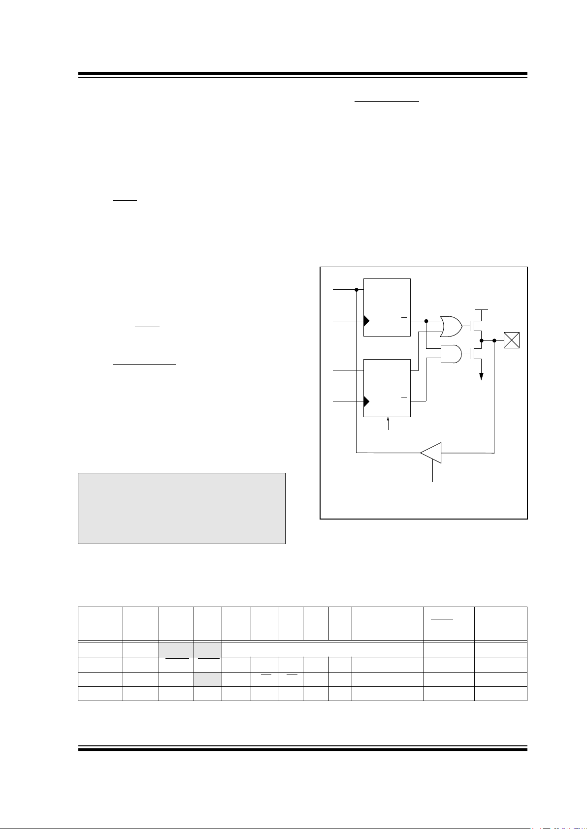
5.1 GPIO
GPIO is an 8-bit I/O register. Only the low order 6 bits
are used (GP5:GP0) for pin control. Bits 6 and 7 (SDA
and SCL) are used by the EEPROM peripheral. Refer
to Section 6.0 and Appendix A for use of SDA and
SCL. Please note that GP3 is an input only pin. The
configuration word can set several I/O’s to alternate
functions. When acting as alternate functions the pins
will read as ‘0’ dur ing port read. Pins GP0, GP1, and
GP3 can be configured with weak pull-ups and also
with wake-up on change. The wake-up on change and
weak pull-up functions are not pin selectable. If pin 4 is
configured as MCLR
, weak pull-up is always on and
wake-up on change for this pin is not enabled.
5.2 TRIS Register
The output driver control register is loaded with the
contents of the W register by executing the TRIS f
instruction. A '1' from a TRIS register bit puts the
corresponding output driver in a hi-impedance mode.
A '0' puts the contents of the output data latch on the
selected pins, enabling the output buffer. The
exceptions are GP3 which is input only and GP2 which
may be controlled by the option register, see Figure 4-
5.
The TRIS registers are “write-only” and are set (output
drivers disabled) upon RESET.
Note: A read of the por ts reads the pins, not the
output data latches. That is, if an output
driver on a pin is enabled and driven high,
but the external system is holding it low, a
read of the port will indicate that the pin is
low.
5.3 I/O Interfacing
The equivalent circuit for an I/O port pin is shown in
Figure 5-1. All port pins, except GP3 which is input
only, may be used for both input and output
operations. For input operations these ports are nonlatching. Any input must be present until read by an
input instruction (e.g., MOVF GPIO,W). The outputs are
latched and remain unchanged until the output latch is
rewritten. To use a port pin as output, the
corresponding direction control bit in TRIS must be
cleared (= 0). For use as an input, the corresponding
TRIS bit must be set. Any I/O pin (except GP3) can be
programmed individually as input or output.
FIGURE 5-1: EQUIVALENT CIRCUIT
FOR A SINGLE I/O PIN
Note 1: I/O pins have protection diodes to VDD and VSS.
Data
Bus
QD
Q
CK
QD
Q
CK
P
N
WR
Port
TRIS ‘f’
Data
TRIS
RD Port
VSS
VDD
I/O
pin
(1)
W
Reg
Latch
Latch
Reset
TABLE 5-1: SUMMARY OF PORT REGISTERS
Address Name Bit 7 Bit 6 Bit 5 Bit 4 Bit 3 Bit 2 Bit 1 Bit 0
Value on
Power-On
Reset
Value on
MCLR and
WDT Reset
Value on
Wake-up on
Pin Change
N/A TRIS — — I/O control registers --11 1111 --11 1111 --11 1111
N/A
OPTION GPWU GPPU T0CS T0SE PSA PS2 PS1 PS0
1111 1111 1111 1111 1111 1111
03H
STATUS
GPWUF — PA0 TO PD Z DC C 0001 1xxx 000q quuu 100q quuu
06h
GPIO
SCL SDA GP5 GP4 GP3 GP2 GP1 GP0 11xx xxxx 11uu uuuu 11uu uuuu
Legend: Shaded cells not used by Port Registers, read as ‘0’, — = unimplemented, read as '0', x = unknown, u = unchanged,
q = see tables in Section 8.7 for possible values.
12CF5XX_GEBook Page 19 Tuesday, October 21, 1997 8:23 AM
PIC12CE5XX
DS40172A-page 20 Preliminary 1997 Microchip Technology Inc.
5.4 I/O Programming Considerations
5.4.1 BI-DIRECTIONAL I/O PORTS
Some instructions operate internally as read followed
by write operations. The BCF and BSF instructions, for
example, read the entire port into the CPU, execute
the bit operation and re-write the result. Caution must
be used when these instructions are applied to a port
where one or more pins are used as input/outputs. For
example, a BSF operation on bit5 of GPIO will cause all
eight bits of GPIO to be read into the CPU, bit5 to be
set and the GPIO value to be written to the output
latches. If another bit of GPIO is used as a bidirectional I/O pin (say bit0) and it is defined as an
input at this time, the input signal present on the pin
itself would be read into the CPU and rewritten to the
data latch of this particular pin, overwriting the
previous content. As long as the pin stays in the input
mode, no problem occurs. However, if bit0 is switched
into output mode later on, the content of the data latch
may now be unknown.
Example 5-1 shows the effect of two sequential readmodify-write instructions (e.g., BCF, BSF , etc.) on an I/
O port.
A pin actively outputting a high or a low should not be
driven from external devices at the same time in order
to change the level on this pin (“wired-or”, “wired-and”).
The resulting high output currents may damage the
chip.
EXAMPLE 5-1: READ-MODIFY-WRITE
INSTRUCTIONS ON AN
I/O PORT
;Initial GPIO Settings
; GPIO<5:3> Inputs
; GPIO<2:0> Outputs
;
; GPIO latch GPIO pins
; ---------- --------- BCF GPIO, 5 ;--01 -ppp --11 pppp
BCF GPIO, 4 ;--10 -ppp --11 pppp
MOVLW 007h ;
TRIS GPIO ;--10 -ppp --11 pppp
;
;Note that the user may have expected the pin
;values to be --00 pppp. The 2nd BCF caused
;GP5 to be latched as the pin value (High).
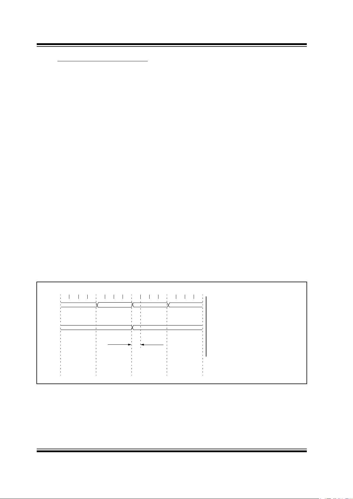
5.4.2 SUCCESSIVE OPERATIONS ON I/O
PORTS
The actual write to an I/O port happens at the end of
an instruction cycle, whereas for reading, the data
must be valid at the beginning of the instruction cycle
(Figure 5-2). Therefore, care must be exercised if a
write followed by a read operation is carried out on the
same I/O port. The sequence of instructions should
allow the pin voltage to stabilize (load dependent)
before the next instruction, which causes that file to be
read into the CPU, is executed. Otherwise, the
previous state of that pin may be read into the CPU
rather than the new state. When in doubt, it is better to
separate these instructions with a NOP or another
instruction not accessing this I/O port.
FIGURE 5-2: SUCCESSIVE I/O OPERATION
PC PC + 1 PC + 2
PC + 3
Q1 Q2
Q3
Q4
Q1 Q2
Q3
Q4
Q1 Q2
Q3
Q4
Q1 Q2
Q3
Q4
Instruction
fetched
GP5:GP0
MOVWF GPIO
NOP
Port pin
sampled here
NOP
MOVF GPIO,W
Instruction
executed
MOVWF GPIO
(Write to
GPIO)
NOP
MOVF GPIO,W
This example shows a write to GPIO followed
by a read from GPIO.
Data setup time = (0.25 TCY – TPD)
where: T
CY = instruction cycle.
TPD = propagation delay
Therefore, at higher clock frequencies, a
write followed by a read may be problematic.
(Read
GPIO)
Port pin
written here
12CF5XX_GEBook Page 20 Tuesday, October 21, 1997 8:23 AM

1997 Microchip Technology Inc. Preliminary DS40172A-page 21
PIC12CE5XX
6.0 EEPROM PERIPHERAL
OPERATION
The PIC12CE518 and PIC12CE519 each have 16
bytes of EEPROM data memory. The EEPROM memory has an endurance of 1,000,000 erase/write cycles
and a data retention of greater than 40 years. The
EEPROM data memory supports a bi-directional 2-wire
bus and data transmission protocol. These two-wires
are serial data (SDA) and serial clock (SCL), that are
mapped to bit6 and bit7, respectively, of the GPIO register (SFR 06h). Unlike the GP0-GP5 that are connected to the I/O pins, SDA and SCL are only
connected to the internal EEPROM peripheral. For
most applications, all that is required is calls to the following functions:
; Byte_Write: Byte write routine
; Inputs: EEPROM Address EEADDR
; EEPROM Data EEDATA
; Outputs: Return 01 in W if OK, else
return 00 in W
;
; Read_Current: Read EEPROM at address
currently held by EE device.
; Inputs: NONE
; Outputs: EEPROM Data EEDATA
; Return 01 in W if OK, else
return 00 in W
;
; Read_Random: Read EEPROM byte at supplied
address
; Inputs: EEPROM Address EEADDR
; Outputs: EEPROM Data EEDATA
; Return 01 in W if OK,
else return 00 in W
The code for these functions is listed in Appendix A,
and is accessed by either including the source code
EEPROM.INC or by linking EEPROM.ASM.
6.0.1 SERIAL DATA
SDA is a bi-directional pin used to transfer addresses
and data into and data out of the device.
For normal data transfer SD A is allowed to change only
during SCL low. Changes during SCL high are
reserved for indicating the START and STOP conditions.
6.0.2 SERIAL CLOCK
This SCL input is used to synchronize the data tr ansf er
from and to the device.
6.1 BUS CHARACTERISTICS
The following bus protocol is to be used with the
EEPROM data memory.
• Data transfer may be initiated only when the bus
is not busy.
During data transfer, the data line must remain stable
whenever the clock line is HIGH. Changes in the data
line while the clock line is HIGH will be interpreted as a
START or STOP condition.
Accordingly, the following bus conditions have been
defined (Figure 6-1).
6.1.1 BUS NOT BUSY (A)
Both data and clock lines remain HIGH.
6.1.2 START DATA TRANSFER (B)
A HIGH to LOW transition of the SDA line while the
clock (SCL) is HIGH determines a START condition. All
commands must be preceded by a START condition.
6.1.3 STOP DATA TRANSFER (C)
A LOW to HIGH transition of the SDA line while the
clock (SCL) is HIGH determines a STOP condition. All
operations must be ended with a STOP condition.
6.1.4 DATA VALID (D)
The state of the data line represents valid data when,
after a START condition, the data line is stable for the
duration of the HIGH period of the clock signal.
The data on the line must be changed during the LOW
period of the clock signal. There is one bit of data per
clock pulse.
Each data transfer is initiated with a START condition
and terminated with a STOP condition. The number of
the data bytes transferred between the START and
STOP conditions is determined by the master device
and is theoretically unlimited.
6.1.5 ACKNOWLEDGE
Each receiving device, when addressed, is obliged to
generate an acknowledge after the reception of each
byte. The master device must generate an extra clock
pulse which is associated with this acknowledge bit.
The device that acknowledges has to pull down the
SDA line during the acknowledge cloc k pulse in such a
way that the SDA line is stable LOW during the HIGH
period of the acknowledge related clock pulse. Of
course, setup and hold times must be taken into
account. A master must signal an end of data to the
slave by not generating an acknowledge bit on the last
byte that has been clocked out of the sla ve. In this case,
the slave must leave the data line HIGH to enable the
master to generate the STOP condition (Figure 6-2).
Note: Acknowledge bits are generated if an inter-
nal programming cycle is in progress.
12CF5XX_GEBook Page 21 Tuesday, October 21, 1997 8:23 AM
PIC12CE5XX
DS40172A-page 22 Preliminary 1997 Microchip Technology Inc.
FIGURE 6-1: DATA TRANSFER SEQUENCE ON THE SERIAL BUS
FIGURE 6-2: ACKNOWLEDGE TIMING
(A)
(B)
(C)
(D)
(A)(C)
SCL
SDA
START
CONDITION
ADDRESS OR
ACKNOWLEDGE
VALID
DATA
ALLOWED
TO CHANGE
STOP
CONDITION
SCL
987654321 1 2 3
Transmitter must release the SDA line at this point
allowing the Receiver to pull the SDA line low to
acknowledge the previous eight bits of data.
Receiver must release the SDA line at this point
so the Transmitter can continue sending data.
Data from transmitter
Data from transmitter
SDA
Acknowledge
Bit
6.2 Device Addressing
After generating a START condition, the bus master
transmits a control byte consisting of a slave address
and a Read/Wr
ite bit that indicates what type of operation is to be performed. The slave address consists of a
4-bit device code (1010) followed by three don't care
bits.
The last bit of the control byte determines the operation
to be performed. When set to a one a read operation is
selected, and when set to a zero a write operation is
selected. (Figure 6-3). The bus is monitored for its corresponding slave address all the time. It generates an
acknowledge bit if the slave address was true and it is
not in a programming mode.
FIGURE 6-3: CONTROL BYTE FORMAT
1 0 1 0 X X XS ACKR/W
Device Select
Bits
Don’t Care
Bits
Slave Address
Acknowledge Bit
Start Bit
Read/Wr
ite Bit
12CF5XX_GEBook Page 22 Tuesday, October 21, 1997 8:23 AM
1997 Microchip Technology Inc. Preliminary DS40172A-page 23
PIC12CE5XX
6.3 WRITE OPERATIONS
6.3.1 BYTE WRITE
Following the start signal from the master, the device
code (4 bits), the don't care bits (3 bits), and the R/W
bit (which is a logic low) are placed onto the bus by the
master transmitter. This indicates to the addressed
slave receiver that a b yte with a word address will follo w
after it has generated an acknowledge bit during the
ninth clock cycle. Therefore, the next byte transmitted
by the master is the word address and will be written
into the address pointer. Only the lower four address
bits are used by the device, and the upper four bits are
don’t cares. The address byte is acknowledgeable and
the master device will then transmit the data word to be
written into the addressed memory location. The memory acknowledges again and the master generates a
stop condition. This initiates the internal write cycle,
and during this time will not generate acknowledge signals (Figure 6-5). After a byte write command, the internal address counter will not be incremented and will
point to the same address location that was just written.
If a stop bit is transmitted to the device at any point in
the write command sequence before the entire
sequence is complete, then the command will abort
and no data will be written. If more than 8 data bits are
transmitted before the stop bit is sent, then the device
will clear the previously loaded byte and begin loading
the data buffer again. If more than one data byte is
transmitted to the device and a stop bit is sent before a
full eight data bits have been transmitted, then the write
command will abort and no data will be written. The
EEPROM memory employs a V
CC threshold detector
circuit which disables the internal erase/write logic if
the V
CC is below minimum VDD.
6.4 ACKNOWLEDGE POLLING
Since the device will not acknowledge during a write
cycle, this can be used to determine when the cycle is
complete (this feature can be used to maximize bus
throughput). Once the stop condition for a write command has been issued from the master, the device initiates the internally timed write cycle. ACK polling can
be initiated immediately . This inv olv es the master sending a start condition followed by the control byte for a
write command (R/W
= 0). If the de vice is still b usy with
the write cycle, then no ACK will be returned. If no A CK
is returned, then the start bit and control byte must be
re-sent. If the cycle is complete, then the device will
return the ACK and the master can then proceed with
the next read or write command. See Figure 6-4 for
flow diagram.
FIGURE 6-4: ACKNOWLEDGE POLLING
FLOW
Send
Write Command
Send Stop
Condition to
Initiate Write Cycle
Send Start
Send Control Byte
with R/W = 0
Did Device
Acknowledge
(ACK = 0)?
Next
Operation
NO
YES
FIGURE 6-5: BYTE WRITE
S
P
BUS ACTIVITY
MASTER
SDA LINE
BUS ACTIVITY
S
T
A
R
T
S
T
O
P
CONTROL
BYTE
WORD
ADDRESS
DATA
A
C
K
A
C
K
A
C
K
1 0 X1 0 XX X
X = Don’t Care Bit
X X X
0
12CF5XX_GEBook Page 23 Tuesday, October 21, 1997 8:23 AM

PIC12CE5XX
DS40172A-page 24 Preliminary 1997 Microchip Technology Inc.
6.5 READ OPERATIONs
Read operations are initiated in the same way as write
operations with the exception that the R/W
bit of the
slave address is set to one. There are three basic types
of read operations: current address read, random read,
and sequential read.
6.5.1 CURRENT ADDRESS READ
It contains an address counter that maintains the
address of the last word accessed, internally incremented by one. Therefore, if the previous read access
was to address n, the next current address read operation would access data from address n + 1. Upon
receipt of the slave address with the R/W
bit set to one,
the device issues an acknowledge and transmits the
eight bit data word. The master will not acknowledge
the transfer but does generate a stop condition and the
device discontinues transmission (Figure 6-6).
6.5.2 RANDOM READ
Random read operations allow the master to access
any memory location in a random manner. To perform
this type of read operation, first the word address must
be set. This is done by sending the word address to the
device as part of a write operation. After the word
address is sent, the master generates a start condition
following the acknowledge. This terminates the write
operation, but not before the internal address pointer is
set. Then the master issues the control byte again but
with the R/W
bit set to a one. It will then issue an
acknowledge and transmits the eight bit data word. The
master will not acknowledge the transf er b ut does generate a stop condition and the device discontinues
transmission (Figure 6-7). After this command, the
internal address counter will point to the address location following the one that was just read.
6.5.3 SEQUENTIAL READ
Sequential reads are initiated in the same way as a ran-
dom read except that after the device transmits the first
data byte, the master issues an acknowledge as
opposed to a stop condition in a random read. This
directs the device to transmit the next sequentially
addressed 8-bit word (Figure 6-8).
To provide sequential reads, it contains an internal
address pointer which is incremented by one at the
completion of each read operation. This address
pointer allows the entire memory contents to be serially
read during one operation.
FIGURE 6-6: CURRENT ADDRESS READ
FIGURE 6-7: RANDOM READ
FIGURE 6-8: SEQUENTIAL READ
BUS ACTIVITY
MASTER
SDA LINE
BUS ACTIVITY
P
S
S
T
O
P
CONTROL
BYTE
S
T
A
R
T
DATA
A
C
K
N
O
A
C
K
1 10 0 X X X 1
X = Don’t Care Bit
P
BUS ACTIVITY
MASTER
SDA LINE
BUS ACTIVITY
S
T
A
R
T
S
T
O
P
CONTROL
BYTE
A
C
K
WORD
ADDRESS (n)
CONTROL
BYTE
S
T
A
R
T
DATA (n)
A
C
K
A
C
K
N
O
A
C
K
X X X X
S 1 10 0 X X X 0
S 1 10 0 X X X 1
X = Don’t Care Bit
P
BUS ACTIVITY
MASTER
SDA LINE
BUS ACTIVITY
S
T
O
P
CONTROL
BYTE
A
C
K
N
O
A
C
K
DATA n DATA n + 1 DATA n + 2 DATA n + X
A
C
K
A
C
K
A
C
K
12CF5XX_GEBook Page 24 Tuesday, October 21, 1997 8:23 AM
1997 Microchip Technology Inc. Preliminary DS40172A-page 25
PIC12CE5XX
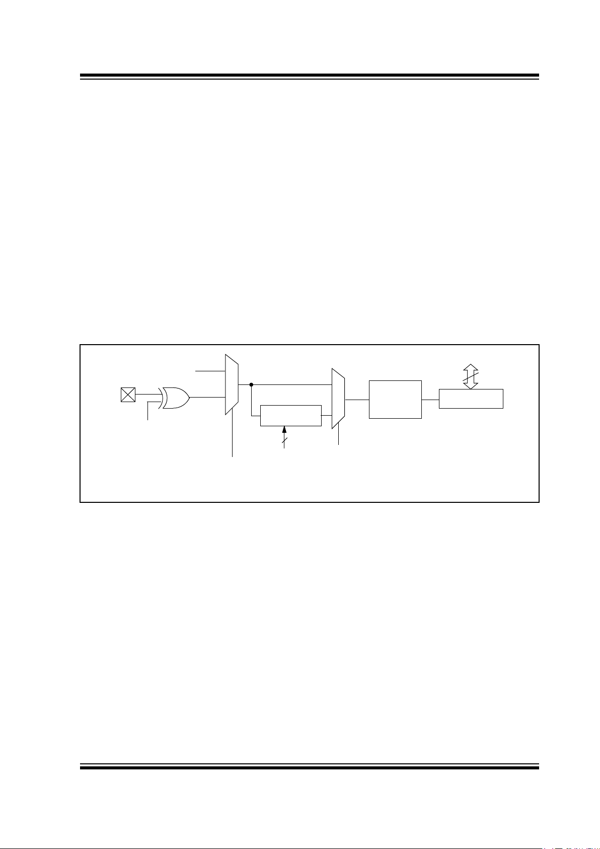
7.0 TIMER0 MODULE AND
TMR0 REGISTER
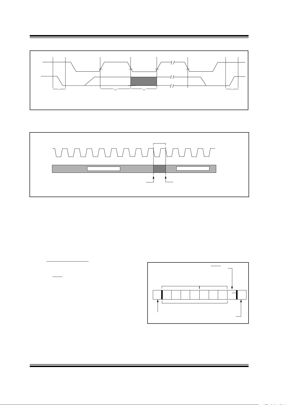
The Timer0 module has the following features:
• 8-bit timer/counter register, TMR0
- Readable and writable
• 8-bit software programmable prescaler
• Internal or external clock select
- Edge select for external clock
Figure 7-1 is a simplified block diagram of the Timer0
module.
Timer mode is selected by clearing the T0CS bit
(OPTION<5>). In timer mode, the Timer0 module will
increment every instruction cycle (without prescaler). If
TMR0 register is written, the increment is inhibited for
the following two cycles (Figure 7-2 and Figure 7-3).
The user can work around this by writing an adjusted
value to the TMR0 register.
Counter mode is selected by setting the T0CS bit
(OPTION<5>). In this mode, Timer0 will increment
either on every rising or falling edge of pin T0CKI. The
T0SE bit (OPTION<4>) determines the source edge.
Clearing the T0SE bit selects the rising edge.
Restrictions on the external clock input are discussed
in detail in Section 7.1.
The prescaler may be used by either the Timer0
module or the Watchdog Timer, but not both. The
prescaler assignment is controlled in software by the
control bit PSA (OPTION<3>). Clearing the PSA bit
will assign the prescaler to Timer0. The prescaler is
not readable or writable. When the prescaler is
assigned to the Timer0 module, prescale v alues of 1:2,
1:4,..., 1:256 are selectable. Section 7.2 details the
operation of the prescaler.
A summary of registers associated with the Timer0
module is found in Table 7-1.
FIGURE 7-1: TIMER0 BLOCK DIAGRAM
Note 1: Bits T0CS, T0SE, PSA, PS2, PS1 and PS0 are located in the OPTION register.
2: The prescaler is shared with the Watchdog Timer (Figure 7-5).
0
1
1
0
T0CS
(1)
FOSC/4
Programmable
Prescaler
(2)
Sync with
Internal
Clocks
TMR0 reg
PSout
(2 cycle delay)
PSout
Data bus
8
PSA
(1)
PS2, PS1, PS0
(1)
3
Sync
T0SE
GP2/T0CKI
Pin
12CF5XX_GEBook Page 25 Tuesday, October 21, 1997 8:23 AM
PIC12CE5XX
DS40172A-page 26 Preliminary 1997 Microchip Technology Inc.
FIGURE 7-2: TIMER0 TIMING: INTERNAL CLOCK/NO PRESCALE
FIGURE 7-3: TIMER0 TIMING: INTERNAL CLOCK/PRESCALE 1:2
TABLE 7-1: REGISTERS ASSOCIATED WITH TIMER0
Address Name Bit 7 Bit 6 Bit 5 Bit 4 Bit 3 Bit 2 Bit 1 Bit 0
Value on
Power-On
Reset
Value on
MCLR and
WDT Reset
Value on
Wake-up on
Pin Change
01h TMR0 Timer0 - 8-bit real-time clock/counter xxxx xxxx uuuu uuuu
uuuu uuuu
N/A OPTION
GPWU GPPU T0CS T0SE PSA PS2 PS1 PS0 1111 1111 1111 1111
1111 1111
N/A TRIS I/O control registers --11 1111 --11 1111 --11 1111
Legend: Shaded cells not used by Timer0,
- = unimplemented, x = unknown, u = unchanged,
PC-1
Q1 Q2 Q3 Q4
Q1 Q2 Q3 Q4 Q1 Q2 Q3 Q4 Q1 Q2 Q3 Q4 Q1 Q2 Q3 Q4 Q1 Q2 Q3 Q4 Q1 Q2 Q3 Q4 Q1 Q2 Q3 Q4
PC
(Program
Counter)
Instruction
Fetch
Timer0
PC PC+1 PC+2 PC+3 PC+4 PC+5 PC+6
T0
T0+1 T0+2 NT0 NT0 NT0 NT0+1 NT0+2
MOVWF TMR0
MOVF TMR0,W MOVF TMR0,W MOVF TMR0,W MOVF TMR0,W MOVF TMR0,W
Write TMR0
executed
Read TMR0
reads NT0
Read TMR0
reads NT0
Read TMR0
reads NT0
Read TMR0
reads NT0 + 1
Read TMR0
reads NT0 + 2
Instruction
Executed
PC-1
Q1 Q2 Q3 Q4
Q1 Q2 Q3 Q4 Q1 Q2 Q3 Q4 Q1 Q2 Q3 Q4 Q1 Q2 Q3 Q4 Q1 Q2 Q3 Q4 Q1 Q2 Q3 Q4 Q1 Q2 Q3 Q4
PC
(Program
Counter)
Instruction
Fetch
Timer0
PC PC+1 PC+2 PC+3 PC+4 PC+5 PC+6
T0 NT0+1
MOVWF TMR0
MOVF TMR0,W MOVF TMR0,W MOVF TMR0,W MOVF TMR0,W MOVF TMR0,W
Write TMR0
executed
Read TMR0
reads NT0
Read TMR0
reads NT0
Read TMR0
reads NT0
Read TMR0
reads NT0
Read TMR0
reads NT0 + 1
T0+1
NT0
Instruction
Execute
T
0
12CF5XX_GEBook Page 26 Tuesday, October 21, 1997 8:23 AM
1997 Microchip Technology Inc. Preliminary DS40172A-page 27
PIC12CE5XX
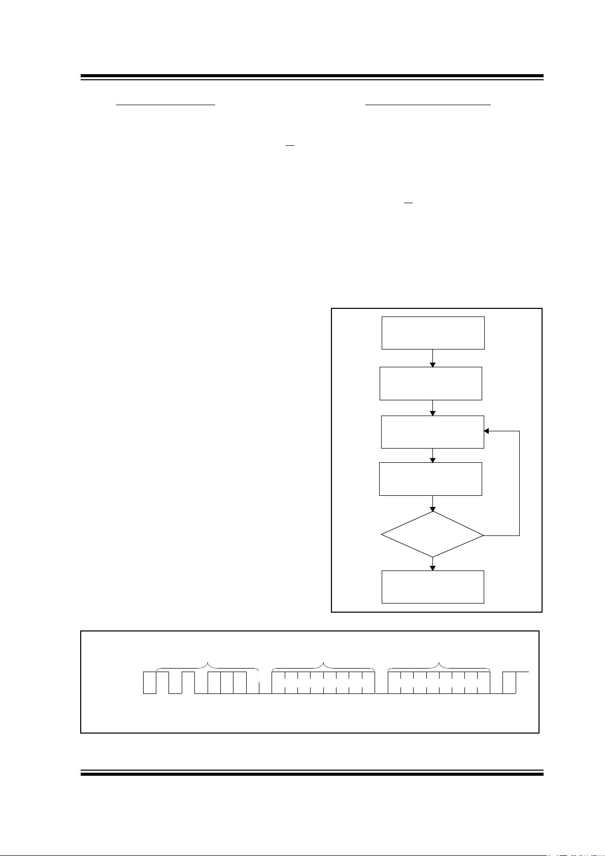
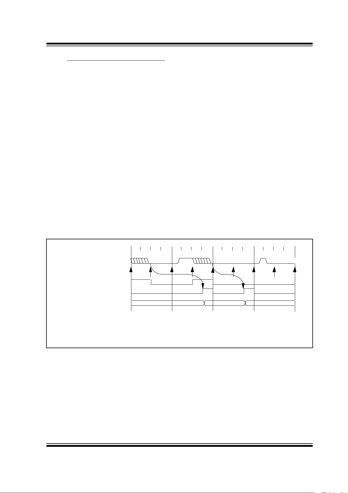
7.1 Using Timer0 with an External Clock
When an external clock input is used for Timer0, it
must meet certain requirements. The external clock
requirement is due to internal phase clock (T
OSC)
synchronization. Also, there is a delay in the actual
incrementing of Timer0 after synchronization.
7.1.1 EXTERNAL CLOCK SYNCHRONIZATION
When no prescaler is used, the external clock input is
the same as the prescaler output. The synchronization
of T0CKI with the internal phase clocks is
accomplished by sampling the prescaler output on the
Q2 and Q4 cycles of the internal phase clocks
(Figure 7-4). Therefore, it is necessary for T0CKI to be
high for at least 2T
OSC (and a small RC delay of 20 ns)
and low for at least 2T
OSC (and a small RC delay of
20 ns). Refer to the electrical specification of the
desired device.
When a prescaler is used, the external clock input is
divided by the asynchronous ripple counter-type
prescaler so that the prescaler output is symmetrical.
For the external clock to meet the sampling
requirement, the ripple counter must be taken into
account. Therefore, it is necessary for T0CKI to have a
period of at least 4T
OSC (and a small RC delay of
40 ns) divided by the prescaler value. The only
requirement on T0CKI high and low time is that they
do not violate the minimum pulse width requirement of
10 ns. Refer to parameters 40, 41 and 42 in the
electrical specification of the desired device.
7.1.2 TIMER0 INCREMENT DELAY
Since the prescaler output is synchronized with the
internal clocks, there is a small delay from the time the
external clock edge occurs to the time the Timer0
module is actually incremented. Figure 7-4 shows the
delay from the external clock edge to the timer
incrementing.
7.1.3 OPTION REGISTER EFFECT ON GP2 TRIS
If the option register is set to read TIMER0 from the pin,
the port is forced to an input regardless of the TRIS register setting.
FIGURE 7-4: TIMER0 TIMING WITH EXTERNAL CLOCK
Increment Timer0 (Q4)
External Clock Input or
Q1 Q2 Q3 Q4 Q1 Q2 Q3 Q4 Q1 Q2 Q3 Q4 Q1 Q2 Q3 Q4
Timer0
T0 T0 + 1 T0 + 2
Small pulse
misses sampling
External Clock/Prescaler
Output After Sampling
(3)
Note 1:
2:
3:
Delay from clock input change to Timer0 increment is 3Tosc to 7Tosc. (Duration of Q = Tosc).
Therefore, the error in measuring the interval between two edges on Timer0 input = ± 4Tosc max.
External clock if no prescaler selected, Prescaler output otherwise.
The arrows indicate the points in time where sampling occurs.
Prescaler Output (2)
(1)
12CF5XX_GEBook Page 27 Tuesday, October 21, 1997 8:23 AM
 Loading...