


Microchip Technology Inc PIC16C84-04-P, PIC16C84-04-SO, PIC16C84-04I-P, PIC16C84-04I-SO, PIC16C84-10-P Datasheet
...M PIC16C84
8-bit CMOS EERPOM Microcontroller
High Performance RISC CPU Features:
•Only 35 single word instructions to learn
•All instructions single cycle (400 ns @ 10 MHz) except for program branches which are two-cycle
•Operating speed: DC - 10 MHz clock input
DC - 400 ns instruction cycle
•14-bit wide instructions
•8-bit wide data path
•1K x 14 EEPROM program memory
•36 x 8 general purpose registers (SRAM)
•64 x 8 on-chip EEPROM data memory
•15 special function hardware registers
•Eight-level deep hardware stack
•Direct, indirect and relative addressing modes
•Four interrupt sources:
-External RB0/INT pin
-TMR0 timer overflow
-PORTB<7:4> interrupt on change
-Data EEPROM write complete
•1,000,000 data memory EEPROM ERASE/WRITE cycles
•EEPROM Data Retention > 40 years
Peripheral Features:
•13 I/O pins with individual direction control
•High current sink/source for direct LED drive
-25 mA sink max. per pin
-20 mA source max. per pin
•TMR0: 8-bit timer/counter with 8-bit programmable prescaler
Special Microcontroller Features:
•Power-on Reset (POR)
•Power-up Timer (PWRT)
•Oscillator Start-up Timer (OST)
•Watchdog Timer (WDT) with its own on-chip RC oscillator for reliable operation
•Code protection
•Power saving SLEEP mode
•Selectable oscillator options
•Serial In-System Programming - via two pins
Pin Diagram
PDIP, SOIC
RA2 |
•1 |
|
18 |
RA1 |
|
RA3 |
2 |
PIC16C84 |
17 |
RA0 |
|
RA4/T0CKI |
3 |
16 |
OSC1/CLKIN |
||
|
|||||
MCLR |
4 |
|
15 |
OSC2/CLKOUT |
|
VSS |
5 |
|
14 |
VDD |
|
RB0/INT |
6 |
|
13 |
RB7 |
|
RB1 |
7 |
|
12 |
RB6 |
|
RB2 |
8 |
|
11 |
RB5 |
|
RB3 |
9 |
|
10 |
RB4 |
CMOS Technology:
•Low-power, high-speed CMOS EEPROM technology
•Fully static design
•Wide operating voltage range:
-Commercial: 2.0V to 6.0V
- Industrial: 2.0V to 6.0V
•Low power consumption:
-< 2 mA typical @ 5V, 4 MHz
-60 A typical @ 2V, 32 kHz
-26 A typical standby current @ 2V
1997 Microchip Technology Inc. |
DS30445C-page 1 |

PIC16C84 |
|
|
Table of Contents |
|
|
1.0 |
General Description ....................................................................................................................................................................... |
3 |
2.0 |
PIC16C84 Device Varieties ........................................................................................................................................................... |
5 |
3.0 |
Architectural Overview ................................................................................................................................................................... |
7 |
4.0 |
Memory Organization................................................................................................................................................................... |
11 |
5.0 |
I/O Ports....................................................................................................................................................................................... |
19 |
6.0 |
Timer0 Module and TMR0 Register............................................................................................................................................. |
25 |
7.0 |
Data EEPROM Memory............................................................................................................................................................... |
31 |
8.0 |
Special Features of the CPU ....................................................................................................................................................... |
35 |
9.0 |
Instruction Set Summary.............................................................................................................................................................. |
51 |
10.0 |
Development Support .................................................................................................................................................................. |
67 |
11.0 |
Electrical Characteristics for PIC16C84....................................................................................................................................... |
71 |
12.0 |
DC & AC Characteristics Graphs/Tables for PIC16C84 .............................................................................................................. |
83 |
13.0 |
Packaging Information ................................................................................................................................................................. |
97 |
Appendix A: Feature Improvements - From PIC16C5X To PIC16C84 ............................................................................................ |
99 |
|
Appendix B: Code Compatibility - from PIC16C5X to PIC16C84.................................................................................................... |
99 |
|
Appendix C: What’s New In This Data Sheet ................................................................................................................................. |
100 |
|
Appendix D: What’s Changed In This Data Sheet ......................................................................................................................... |
100 |
|
Appendix E: Conversion Considerations - PIC16C84 to PIC16F83/F84 And PIC16CR83/CR84.................................................. |
101 |
|
Index .................................................................................................................................................................................................. |
103 |
|
On-Line Support................................................................................................................................................................................. |
105 |
|
PIC16C84 Product Identification System ........................................................................................................................................... |
107 |
|
Sales and Support.............................................................................................................................................................................. |
107 |
|
To Our Valued Customers
We constantly strive to improve the quality of all our products and documentation. We have spent a great deal of time to ensure that these documents are correct. However, we realize that we may have missed a few things. If you find any information that is missing or appears in error, please use the reader response form in the back of this data sheet to inform us. We appreciate your assistance in making this a better document.
DS30445C-page 2 |
1997 Microchip Technology Inc. |

PIC16C84
1.0GENERAL DESCRIPTION
The PIC16C84 is a low-cost, high-performance, CMOS, fully-static, 8-bit microcontroller.
All PIC16/17 microcontrollers employ an advanced RISC architecture. PIC16CXX devices have enhanced core features, eight-level deep stack, and multiple internal and external interrupt sources. The separate instruction and data buses of the Harvard architecture allow a 14-bit wide instruction word with a separate 8-bit wide data bus. The two stage instruction pipeline allows all instructions to execute in a single cycle, except for program branches (which require two cycles). A total of 35 instructions (reduced instruction set) are available. Additionally, a large register set is used to achieve a very high performance level.
PIC16CXX microcontrollers typically achieve a 2:1 code compression and up to a 2:1 speed improvement (at 10 MHz) over other 8-bit microcontrollers in their class.
The PIC16C84 has 36 bytes of RAM, 64 bytes of Data EEPROM memory, and 13 I/O pins. A timer/counter is also available.
The PIC16CXX family has special features to reduce external components, thus reducing cost, enhancing system reliability and reducing power consumption. There are four oscillator options, of which the single pin RC oscillator provides a low-cost solution, the LP oscillator minimizes power consumption, XT is a standard crystal, and the HS is for High Speed crystals. The SLEEP (power-down) mode offers power savings. The user can wake the chip from sleep through several external and internal interrupts and resets.
A highly reliable Watchdog Timer with its own on-chip RC oscillator provides protection against software lockup.
The PIC16C84 EEPROM program memory allows the same device package to be used for prototyping and production. In-circuit reprogrammability allows the code to be updated without the device being removed from the end application. This is useful in the development of many applications where the device may not be easily accessible, but the prototypes may require code updates. This is also useful for remote applications where the code may need to be updated (such as rate information).
Table 1-1 lists the features of the PIC16C84. A simplified block diagram of the PIC16C84 is shown in Figure 3-1.
The PIC16C84 fits perfectly in applications ranging from high speed automotive and appliance motor control to low-power remote sensors, electronic locks, security devices and smart cards. The EEPROM technology makes customization of application programs (transmitter codes, motor speeds, receiver frequencies, security codes, etc.) extremely fast and convenient. The small footprint packages make this microcontroller series perfect for all applications with space limitations. Low cost, low power, high performance, ease of use and I/O flexibility make the PIC16C84 very versatile even in areas where no microcontroller use has been considered before (e.g., timer functions, serial communication, capture and compare, PWM functions and co-processor applications).
The serial in-system programming feature (via two pins) offers flexibility of customizing the product after complete assembly and testing. This feature can be used to serialize a product, store calibration data, or program the device with the current firmware before shipping.
1.1Family and Upward Compatibility
Those users familiar with the PIC16C5X family of microcontrollers will realize that this is an enhanced version of the PIC16C5X architecture. Please refer to Appendix A for a detailed list of enhancements. Code written for PIC16C5X can be easily ported to the PIC16C84 (Appendix B).
1.2Development Support
The PIC16CXX family is supported by a full-featured macro assembler, a software simulator, an in-circuit emulator, a low-cost development programmer and a full-featured programmer. A “C”compiler and fuzzy logic support tools are also available.
1997 Microchip Technology Inc. |
DS30445C-page 3 |

PIC16C84
TABLE 1-1 |
PIC16C8X FAMILY OF DEVICES |
|
|
|
||
|
|
|
|
|
|
|
|
|
|
PIC16F83 |
PIC16CR83 |
PIC16F84 |
PIC16CR84 |
|
|
|
|
|
|
|
Clock |
|
Maximum Frequency |
10 |
10 |
10 |
10 |
|
of Operation (MHz) |
|
|
|
|
|
|
|
|
|
|
|
|
|
|
|
|
|
|
|
|
|
Flash Program Memory |
512 |
— |
1K |
— |
|
|
|
|
|
|
|
|
|
EEPROM Program Memory |
— |
— |
— |
— |
Memory |
|
|
|
|
|
|
|
ROM Program Memory |
— |
512 |
— |
1K |
|
|
|
|
|
|
|
|
|
|
Data Memory (bytes) |
36 |
36 |
68 |
68 |
|
|
|
|
|
|
|
|
|
Data EEPROM (bytes) |
64 |
64 |
64 |
64 |
Peripherals |
|
|
|
|
|
|
|
Timer Module(s) |
TMR0 |
TMR0 |
TMR0 |
TMR0 |
|
|
|
|
|
|
|
|
|
|
Interrupt Sources |
4 |
4 |
4 |
4 |
|
|
|
|
|
|
|
|
|
I/O Pins |
13 |
13 |
13 |
13 |
Features |
|
|
|
|
|
|
|
Voltage Range (Volts) |
2.0-6.0 |
2.0-6.0 |
2.0-6.0 |
2.0-6.0 |
|
|
|
|
|
|
|
|
|
|
Packages |
18-pin DIP, |
18-pin DIP, |
18-pin DIP, |
18-pin DIP, |
|
|
|
SOIC |
SOIC |
SOIC |
SOIC |
|
|
|
|
|
|
|
All PICmicro™ F amily devices have Power-on Reset, selectable Watchdog Timer, selectable code protect and high I/O current capability. All PIC16C8X Family devices use serial programming with clock pin RB6 and data pin RB7.
DS30445C-page 4 |
1997 Microchip Technology Inc. |

PIC16C84
2.0PIC16C84 DEVICE VARIETIES
A variety of frequency ranges and packaging options are available. Depending on application and production requirements the proper device option can be selected using the information in this section. When placing orders, please use the “PIC16C84 Product Identification System” at the back of this data sheet to specify the correct part number.
There are two device “types”as indicated in the device number.
1.C, as in PIC16C84. These devices have EEPROM program memory and operate over the standard voltage range.
2.LC, as in PIC16LC84. These devices have EEPROM program memory and operate over an extended voltage range.
When discussing memory maps and other architectural features, the use of C also implies the LC versions.
2.1Electrically Erasable Devices
These devices are offered in the lower cost plastic package, even though the device can be erased and reprogrammed. This allows the same device to be used for prototype development and pilot programs as well as production.
A further advantage of the electrically erasable version is that they can be erased and reprogrammed in-circuit, or by device programmers, such as Microchip's PICSTART Plus or PRO MATE II programmers.
1997 Microchip Technology Inc.
DS30445C-page 5

PIC16C84
NOTES:
DS30445C-page 6 |
1997 Microchip Technology Inc. |

PIC16C84
3.0ARCHITECTURAL OVERVIEW
The high performance of the PIC16CXX family can be attributed to a number of architectural features commonly found in RISC microprocessors. To begin with, the PIC16CXX uses a Harvard architecture. This architecture has the program and data accessed from separate memories. So the device has a program memory bus and a data memory bus. This improves bandwidth over traditional von Neumann architecture where program and data are fetched from the same memory (accesses over the same bus). Separating program and data memory further allows instructions to be sized differently than the 8-bit wide data word. PIC16CXX opcodes are 14-bits wide, enabling single word instructions. The full 14-bit wide program memory bus fetches a 14-bit instruction in a single cycle. A twostage pipeline overlaps fetch and execution of instructions (Example 3-1). Consequently, all instructions execute in a single cycle (400 ns @ 10 MHz) except for program branches.
The PIC16C84 addresses 1K x 14 program memory. All program memory is internal.
PIC16CXX devices can directly or indirectly address its register files or data memory. All special function registers including the program counter are mapped in the data memory. An orthogonal (symmetrical) instruction set that makes it possible to carry out any operation on any register using any addressing mode. This symmetrical nature and lack of ‘special optimal situations’ make programming with the PIC16CXX simple yet efficient. In addition, the learning curve is reduced significantly.
The PIC16C84 has 36 x 8 SRAM and 64 x 8 EEPROM data memory.
PIC16CXX devices contain an 8-bit ALU and working register. The ALU is a general purpose arithmetic unit. It performs arithmetic and Boolean functions between data in the working register and any register file.
The ALU is 8-bits wide and capable of addition, subtraction, shift and logical operations. Unless otherwise mentioned, arithmetic operations are two's complement in nature. In two-operand instructions, typically one operand is the working register (W register), and the other operand is a file register or an immediate constant. In single operand instructions, the operand is either the W register or a file register.
The W register is an 8-bit working register used for ALU operations. It is not an addressable register.
Depending on the instruction executed, the ALU may affect the values of the Carry (C), Digit Carry (DC), and Zero (Z) bits in the STATUS register. The C and DC bits operate as a borrow and digit borrow out bit, respectively, in subtraction. See the SUBLW and SUBWF instructions for examples.
A simplified block diagram for the PIC16C84 is shown in Figure 3-1, its corresponding pin description is shown in Table 3-1.
1997 Microchip Technology Inc. |
DS30445C-page 7 |

PIC16C84 |
|
|
|
|
|
|
|
FIGURE 3-1: |
PIC16C84 BLOCK DIAGRAM |
|
|
|
|
||
|
|
13 |
|
Data Bus 8 |
|
|
|
EEPROM |
|
Program Counter |
|
|
EEPROM Data Memory |
||
|
|
|
|
|
|||
Program |
|
|
|
|
|
|
|
Memory |
|
|
|
|
|
|
|
1K x 14 |
|
|
|
RAM |
|
|
EEPROM |
|
8 Level Stack |
File Registers |
EEDATA |
Data Memory |
|||
|
|
||||||
|
|
|
(13-bit) |
36 x 8 |
|
|
64 x 8 |
|
|
|
|
|
|
|
|
Program |
|
|
|
|
|
|
|
Bus 14 |
|
|
|
7 |
RAM Addr |
|
EEADR |
|
|
|
|
|
|||
|
|
|
|
|
|
||
|
|
|
|
|
|
|
|
Instruction reg |
|
|
Addr Mux |
|
|
||
|
|
|
|
|
|
||
|
|
5 |
Direct Addr |
7 |
Indirect |
TMR0 |
|
|
|
|
|
Addr |
|
|
|
|
|
|
|
|
|
|
|
|
|
|
|
FSR reg |
|
|
|
|
|
|
|
STATUS reg |
|
RA4/T0CKI |
|
|
|
|
|
|
|
||
|
|
|
8 |
|
|
|
|
|
|
Power-up |
|
MUX |
|
|
|
|
|
|
|
I/O Ports |
|
||
|
|
Timer |
|
|
|
||
|
|
|
|
|
|
||
Instruction |
Oscillator |
|
|
|
|
||
Decode & |
Start-up Timer |
ALU |
|
|
|
||
Control |
|
|
|
|
|
||
Power-on |
|
|
|
|
|||
|
|
|
|
|
RA3:RA0 |
||
|
|
Reset |
|
|
|
|
|
Timing |
Watchdog |
W reg |
|
|
RB7:RB1 |
||
Generation |
Timer |
|
|
||||
|
|
|
|
||||
|
|
|
|
|
|
|
RB0/INT |
OSC2/CLKOUT |
MCLR |
VDD, VSS |
|
|
|
|
|
OSC1/CLKIN |
|
|
|
|
|
|
|
DS30445C-page 8 |
1997 Microchip Technology Inc. |

|
|
|
|
|
|
|
|
PIC16C84 |
|
|
|
|
|
|
|
|
|
TABLE 3-1 |
PIC16C8X PINOUT DESCRIPTION |
|||||||
|
|
|
|
|
|
|
|
|
|
Pin Name |
|
DIP |
SOIC |
I/O/P |
Buffer |
Description |
|
|
|
No. |
No. |
Type |
Type |
|||
|
|
|
|
|
||||
|
|
|
|
|
|
|
||
|
|
|
|
|
|
|
||
OSC1/CLKIN |
|
16 |
16 |
I |
ST/CMOS (1) |
Oscillator crystal input/external clock source input. |
||
|
OSC2/CLKOUT |
|
15 |
15 |
O |
— |
Oscillator crystal output. Connects to crystal or resonator in crys- |
|
|
|
|
|
|
|
|
|
tal oscillator mode. In RC mode, OSC2 pin outputs CLKOUT which |
|
|
|
|
|
|
|
|
has 1/4 the frequency of OSC1, and denotes the instruction cycle |
|
|
|
|
|
|
|
|
rate. |
|
|
|
|
|
|
|
|
|
|
|
|
|
4 |
4 |
I/P |
ST |
Master clear (reset) input/programming voltage input. This pin is an |
|
MCLR |
|||||||
|
|
|
|
|
|
|
|
active low reset to the device. |
|
|
|
|
|
|
|
|
|
|
|
|
|
|
|
|
|
PORTA is a bi-directional I/O port. |
|
RA0 |
|
17 |
17 |
I/O |
TTL |
|
|
|
RA1 |
|
18 |
18 |
I/O |
TTL |
|
|
|
RA2 |
|
1 |
1 |
I/O |
TTL |
|
|
|
RA3 |
|
2 |
2 |
I/O |
TTL |
|
|
|
RA4/T0CKI |
|
3 |
3 |
I/O |
ST |
Can also be selected to be the clock input to the TMR0 timer/ |
|
|
|
|
|
|
|
|
|
counter. Output is open drain type. |
|
|
|
|
|
|
|
|
|
|
|
|
|
|
|
|
|
PORTB is a bi-directional I/O port. PORTB can be software pro- |
|
|
|
|
|
|
|
|
grammed for internal weak pull-up on all inputs. |
|
RB0/INT |
|
6 |
6 |
I/O |
TTL |
RB0/INT can also be selected as an external interrupt pin. |
|
|
RB1 |
|
7 |
7 |
I/O |
TTL |
|
|
|
RB2 |
|
8 |
8 |
I/O |
TTL |
|
|
|
RB3 |
|
9 |
9 |
I/O |
TTL |
|
|
|
RB4 |
|
10 |
10 |
I/O |
TTL |
Interrupt on change pin. |
|
|
RB5 |
|
11 |
11 |
I/O |
TTL |
Interrupt on change pin. |
|
|
RB6 |
|
12 |
12 |
I/O |
TTL/ST (2) |
Interrupt on change pin. Serial programming clock. |
|
|
RB7 |
|
13 |
13 |
I/O |
TTL/ST (2) |
Interrupt on change pin. Serial programming data. |
|
|
VSS |
|
5 |
5 |
P |
— |
Ground reference for logic and I/O pins. |
|
|
|
|
|
|
|
|
||
VDD |
|
14 |
14 |
P |
— |
Positive supply for logic and I/O pins. |
||
|
|
|
|
|
|
|
|
|
Legend: |
I= input |
O = output |
I/O = Input/Output |
P = power |
|
|
— = Not used |
TTL = TTL input |
ST = Schmitt Trigger input |
Note 1: |
This buffer is a Schmitt Trigger input when configured in RC oscillator mode and a CMOS input otherwise. |
|||
2:This buffer is a Schmitt Trigger input when used in serial programming mode.
1997 Microchip Technology Inc. |
DS30445C-page 9 |
PIC16C84
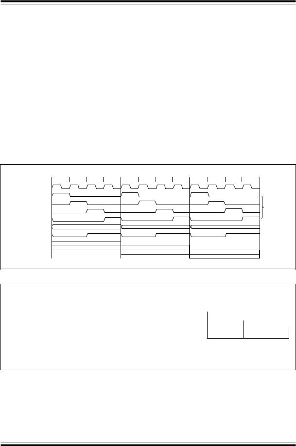
3.1Clocking Scheme/Instruction Cycle
The clock input (from OSC1) is internally divided by four to generate four non-overlapping quadrature clocks namely Q1, Q2, Q3 and Q4. Internally, the program counter (PC) is incremented every Q1, the instruction is fetched from the program memory and latched into the instruction register in Q4. The instruction is decoded and executed during the following Q1 through Q4. The clocks and instruction execution flow is shown in Figure 3-2.
FIGURE 3-2: CLOCK/INSTRUCTION CYCLE
3.2Instruction Flow/Pipelining
An “Instruction Cycle” consists of four Q cycles (Q1, Q2, Q3 and Q4). The instruction fetch and execute are pipelined such that fetch takes one instruction cycle while decode and execute takes another instruction cycle. However, due to the pipelining, each instruction effectively executes in one cycle. If an instruction causes the program counter to change (e.g., GOTO) then two cycles are required to complete the instruction (Example 3-1).
A fetch cycle begins with the Program Counter (PC) incrementing in Q1.
In the execution cycle, the fetched instruction is latched into the “Instruction Register” in cycle Q1. This instruction is then decoded and executed during the Q2, Q3, and Q4 cycles. Data memory is read during Q2 (operand read) and written during Q4 (destination write).
Q1 |
Q2 |
Q3 |
Q4 |
Q1 |
Q2 |
Q3 |
Q4 |
Q1 |
Q2 |
Q3 |
Q4 |
OSC1 |
|
|
|
|
|
|
|
|
|
|
|
Q1 |
|
|
|
|
|
|
|
|
|
|
|
Q2 |
|
|
|
|
|
|
|
|
|
|
Internal |
Q3 |
|
|
|
|
|
|
|
|
|
|
phase |
|
|
|
|
|
|
|
|
|
|
clock |
|
Q4 |
|
|
|
|
|
|
|
|
|
|
|
PC |
|
PC |
|
|
PC+1 |
|
|
|
|
PC+2 |
|
OSC2/CLKOUT |
|
|
|
|
|
|
|
|
|
|
|
(RC mode) |
Fetch INST (PC) |
|
|
|
|
|
|
|
|
|
|
|
|
|
|
|
|
|
|
|
|
||
|
Execute INST (PC-1) |
|
|
Fetch INST (PC+1) |
|
|
|
|
|
||
|
|
|
|
|
Execute INST (PC) |
|
|
Fetch INST (PC+2) |
|
||
|
|
|
|
|
|
|
|
|
Execute INST (PC+1) |
|
|
EXAMPLE 3-1: INSTRUCTION PIPELINE FLOW
1. |
MOVLW |
55h |
Fetch 1 |
Execute 1 |
|
|
|
|
|
|
|
|
|
|
|
|
|
2. |
MOVWF |
PORTB |
|
Fetch 2 |
Execute 2 |
|
|
|
|
|
|
|
|
|
|
|
|
3. |
CALL |
SUB_1 |
|
|
Fetch 3 |
Execute 3 |
|
|
|
|
|
|
|
|
|
|
|
4. |
BSF |
PORTA, BIT3 |
|
|
|
Fetch 4 |
Flush |
|
|
|
|
|
|
|
|
|
|
Fetch SUB_1 Execute SUB_1
All instructions are single cycle, except for any program branches. These take two cycles since the fetch instruction is “flushed” from the pipeline while the new instruction is being fetched and then executed.
DS30445C-page 10 |
1997 Microchip Technology Inc. |
4.0MEMORY ORGANIZATION
There are two memory blocks in the PIC16C84. These are the program memory and the data memory. Each block has its own bus, so that access to each block can occur during the same oscillator cycle.
The data memory can further be broken down into the general purpose RAM and the Special Function Registers (SFRs). The operation of the SFRs that control the “core”are described here. The SFRs used to control the peripheral modules are described in the section discussing each individual peripheral module.
The data memory area also contains the data EEPROM memory. This memory is not directly mapped into the data memory, but is indirectly mapped. That is an indirect address pointer specifies the address of the data EEPROM memory to read/write. The 64 bytes of data EEPROM memory have the address range 0h-3Fh. More details on the EEPROM memory can be found in Section 7.0.
4.1Program Memory Organization
The PIC16CXX has a 13-bit program counter capable of addressing an 8K x 14 program memory space. For the PIC16C84, only the first 1K x 14 (0000h-03FFh) are physically implemented (Figure 4-1). Accessing a location above the physically implemented address will cause a wraparound. For example, locations 20h, 420h, 820h, C20h, 1020h, 1420h, 1820h, and 1C20h will be the same instruction.
The reset vector is at 0000h and the interrupt vector is at 0004h.
PIC16C84
FIGURE 4-1: PROGRAM MEMORY MAP
AND STACK
PC<12:0>
CALL, RETURN |
13 |
|
|
|
||||
|
|
|
|
|||||
RETFIE, RETLW |
|
|
|
|
|
|||
|
|
|
|
|
|
|
|
|
|
|
|
Stack Level 1 |
|
|
|
|
|
|
|
|
• |
|
|
|
|
|
|
|
|
• |
|
|
|
|
|
|
|
|
• |
|
|
|
|
|
|
|
|
|
|
|
|
|
|
|
|
|
Stack Level 8 |
|
|
|
|
|
|
|
|
|
|
|
|
|
|
|
|
|
Reset Vector |
|
0000h |
|
||
|
|
|
|
|
|
|
|
|
|
|
|
Peripheral Interrupt Vector |
0004h |
|
|||
User Memory Space |
|
|
|
|
||||
|
|
|
|
|||||
|
|
|
|
|||||
3FFh |
1FFFh |
1997 Microchip Technology Inc. |
DS30445C-page 11 |
PIC16C84
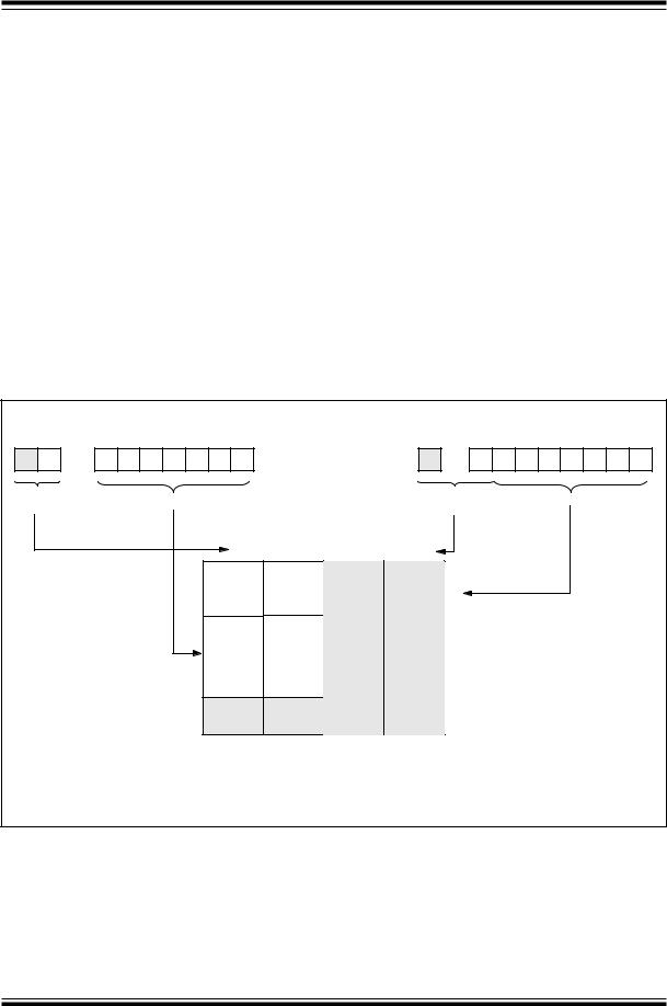
4.2Data Memory Organization
The data memory is partitioned into two areas. The first is the Special Function Registers (SFR) area, while the second is the General Purpose Registers (GPR) area. The SFRs control the operation of the device.
Portions of data memory are banked. This is for both the SFR area and the GPR area. The GPR area is banked to allow greater than 116 bytes of general purpose RAM. The banked areas of the SFR are for the registers that control the peripheral functions. Banking requires the use of control bits for bank selection. These control bits are located in the STATUS Register. Figure 4-2 shows the data memory map organization.
Instructions MOVWF and MOVF can move values from the W register to any location in the register file (“F”), and vice-versa.
The entire data memory can be accessed either directly using the absolute address of each register file or indirectly through the File Select Register (FSR) (Section 4.5). Indirect addressing uses the present value of the RP1:RP0 bits for access into the banked areas of data memory.
Data memory is partitioned into two banks which contain the general purpose registers and the special function registers. Bank 0 is selected by clearing the RP0 bit (STATUS<5>). Setting the RP0 bit selects Bank 1. Each Bank extends up to 7Fh (128 bytes). The first twelve locations of each Bank are reserved for the Special Function Registers. The remainder are General Purpose Registers implemented as static RAM.
4.2.1GENERAL PURPOSE REGISTER FILE
All devices have some amount of General Purpose Register (GPR) area. Each GPR is 8 bits wide and is accessed either directly or indirectly through the FSR (Section 4.5).
The GPR addresses in bank 1 are mapped to addresses in bank 0. As an example, addressing location 0Ch or 8Ch will access the same GPR.
4.2.2SPECIAL FUNCTION REGISTERS
The Special Function Registers (Figure 4-2 and Table 4-1) are used by the CPU and Peripheral functions to control the device operation. These registers are static RAM.
The special function registers can be classified into two sets, core and peripheral. Those associated with the core functions are described in this section. Those related to the operation of the peripheral features are described in the section for that specifi feature.
FIGURE 4-2: REGISTER FILE MAP
File Address |
|
File Address |
||||
00h |
Indirect addr.(1) |
Indirect addr.(1) |
|
|
80h |
|
01h |
TMR0 |
OPTION |
|
|
81h |
|
02h |
|
|
|
|
82h |
|
PCL |
PCL |
|
|
|||
03h |
|
|
|
|
83h |
|
STATUS |
STATUS |
|
|
|||
04h |
|
|
|
|
84h |
|
FSR |
FSR |
|
|
|||
05h |
PORTA |
TRISA |
|
|
85h |
|
06h |
|
|
|
|
86h |
|
PORTB |
TRISB |
|
|
|||
07h |
|
|
|
|
87h |
|
08h |
EEDATA |
EECON1 |
|
|
88h |
|
09h |
EEADR |
EECON2(1) |
|
|
89h |
|
0Ah |
PCLATH |
PCLATH |
|
|
8Ah |
|
0Bh |
|
|
|
|
8Bh |
|
INTCON |
INTCON |
|
|
|||
0Ch |
|
|
|
|
8Ch |
|
|
|
36 |
|
|
|
|
|
|
General |
Mapped |
|
|
|
|
|
Purpose |
(accesses) |
|
|
|
|
|
registers |
in Bank 0 |
|
|
|
|
|
(SRAM) |
|
|
|
|
2Fh |
|
|
|
|
AFh |
|
30h |
|
|
|
|
B0h |
|
|
|
|
|
|
|
|
|
|
|
|
|
|
|
|
|
|
|
|
|
|
|
|
|
|
|
|
|
|
|
|
|
|
|
|
|
|
|
|
|
|
|
|
|
|
|
|
|
|
|
7Fh |
|
|
FFh |
|
|
Bank 0 |
Bank 1 |
|
|
Unimplemented data memory location; read as '0'. |
|||
|
||||
Note 1: |
Not a physical register. |
|||
DS30445C-page 12 |
1997 Microchip Technology Inc. |

PIC16C84
TABLE 4-1 |
REGISTER FILE SUMMARY |
|
|
|
|
|
|
|
|
|
|
|
|
|
|
|
||||||||||
|
|
|
|
|
|
|
|
|
|
|
|
|
|
|
|
|
|
|
|
|
|
|
|
|
||
|
|
|
|
|
|
|
|
|
|
|
|
|
|
|
|
|
|
|
|
|
|
|
Value on |
Value on all |
||
Address |
Name |
|
|
Bit 7 |
Bit 6 |
Bit 5 |
Bit 4 |
|
Bit 3 |
|
Bit 2 |
|
Bit 1 |
|
Bit 0 |
|
Power-on |
other resets |
||||||||
|
|
|
|
|
|
|
|
|
|
|
|
|
|
|
|
|
|
|
|
|
|
|
Reset |
(Note3) |
||
|
|
|
|
|
|
|
|
|
|
|
|
|
|
|
|
|
|
|
|
|
|
|
|
|
||
|
|
|
|
|
|
|
|
|
|
|
|
|
|
|
|
|
|
|
|
|
|
|
||||
|
|
|
|
|
|
|
|
|
|
|
|
Bank 0 |
|
|
|
|
|
|
|
|
|
|
||||
|
|
|
|
|
|
|
|
|
|
|
|
|
|
|
|
|
||||||||||
00h |
INDF |
|
|
|
|
Uses contents of FSR to address data memory (not a physical register) |
|
|
---- ---- |
---- ---- |
||||||||||||||||
|
|
|
|
|
|
|
|
|
|
|
|
|
|
|
|
|
||||||||||
01h |
TMR0 |
|
|
|
|
|
|
8-bit real-time clock/counter |
|
|
|
|
|
|
xxxx xxxx |
uuuu uuuu |
||||||||||
|
|
|
|
|
|
|
|
|
|
|
|
|
|
|
|
|||||||||||
02h |
PCL |
|
|
|
|
|
Low order 8 bits of the Program Counter (PC) |
|
|
|
|
0000 |
0000 |
0000 |
0000 |
|||||||||||
|
|
|
|
|
|
|
|
|
|
|
|
|
|
|
|
|
|
|
|
|
|
|
|
|
|
|
03h |
STATUS (2) |
|
IRP |
RP1 |
RP0 |
|
TO |
|
|
|
PD |
|
|
Z |
|
DC |
|
C |
|
0001 |
1xxx |
000q |
quuu |
|||
04h |
FSR |
|
|
|
|
|
Indirect data memory address pointer 0 |
|
|
|
|
xxxx xxxx |
uuuu uuuu |
|||||||||||||
|
|
|
|
|
|
|
|
|
|
|
|
|
|
|
|
|
|
|
|
|
||||||
05h |
PORTA |
|
|
— |
— |
— |
RA4/T0CKI |
|
RA3 |
|
RA2 |
|
RA1 |
|
RA0 |
|
---x xxxx |
---u uuuu |
||||||||
06h |
PORTB |
|
|
RB7 |
RB6 |
RB5 |
RB4 |
|
RB3 |
|
RB2 |
|
RB1 |
|
RB0/INT |
|
xxxx xxxx |
uuuu uuuu |
||||||||
|
|
|
|
|
|
|
|
|
|
|
|
|
|
|
|
|
|
|
|
|
|
|
||||
07h |
|
|
Unimplemented location, read as '0' |
|
|
|
|
|
|
|
|
|
|
|
---- ---- |
---- ---- |
||||||||||
08h |
EEDATA |
|
|
|
|
|
|
EEPROM data register |
|
|
|
|
|
|
xxxx xxxx |
uuuu uuuu |
||||||||||
|
|
|
|
|
|
|
|
|
|
|
|
|
|
|
|
|
||||||||||
09h |
EEADR |
|
|
|
|
|
|
EEPROM address register |
|
|
|
|
|
|
xxxx xxxx |
uuuu uuuu |
||||||||||
|
|
|
|
|
|
|
|
|
|
|
|
|
|
|
|
|
|
|
||||||||
0Ah |
PCLATH |
|
— |
— |
— |
|
|
|
Write buffer for upper 5 bits of the PC (1) |
|
|
---0 0000 |
---0 0000 |
|||||||||||||
0Bh |
INTCON |
|
GIE |
EEIE |
T0IE |
INTE |
|
RBIE |
|
T0IF |
|
INTF |
|
RBIF |
|
0000 |
000x |
0000 |
000u |
|||||||
|
|
|
|
|
|
|
|
|
|
|
|
|
|
|
|
|
|
|
|
|
|
|
||||
|
|
|
|
|
|
|
|
|
|
|
|
Bank 1 |
|
|
|
|
|
|
|
|
|
|
||||
|
|
|
|
|
|
|
|
|
|
|
|
|
|
|
|
|
||||||||||
80h |
INDF |
|
|
|
|
Uses contents of FSR to address data memory (not a physical register) |
|
|
---- ---- |
---- ---- |
||||||||||||||||
|
|
|
|
|
|
|
|
|
|
|
|
|
|
|
|
|
|
|
|
|
|
|
|
|
||
81h |
OPTION_ |
|
|
|
|
|
|
|
|
|
|
|
|
|
|
|
|
|
|
|
|
1111 |
1111 |
1111 1111 |
||
RBPU |
INTEDG |
T0CS |
T0SE |
|
PSA |
|
PS2 |
|
PS1 |
|
PS0 |
|
||||||||||||||
REG |
|
|
|
|
|
|
|
|
|
|
||||||||||||||||
|
|
|
|
|
|
|
|
|
|
|
|
|
|
|
|
|
|
|
|
|
|
|
|
|
|
|
|
|
|
|
|
|
|
|
|
|
|
|
|
|
|
|
|
|
|
||||||||
82h |
PCL |
|
|
|
|
|
Low order 8 bits of Program Counter (PC) |
|
|
|
|
0000 |
0000 |
0000 0000 |
||||||||||||
|
|
|
|
|
|
|
|
|
|
|
|
|
|
|
|
|
|
|
|
|
|
|
|
|
||
83h |
STATUS (2) |
|
IRP |
RP1 |
RP0 |
|
|
TO |
|
|
|
PD |
|
|
Z |
|
DC |
|
C |
|
0001 |
1xxx |
000q |
quuu |
||
84h |
FSR |
|
|
|
|
|
Indirect data memory address pointer 0 |
|
|
|
|
xxxx xxxx |
uuuu uuuu |
|||||||||||||
|
|
|
|
|
|
|
|
|
|
|
|
|
|
|
|
|
||||||||||
85h |
TRISA |
|
|
— |
— |
— |
PORTA data direction register |
|
|
|
|
---1 1111 |
---1 1111 |
|||||||||||||
86h |
TRISB |
|
|
|
|
|
|
PORTB data direction register |
|
|
|
|
|
|
1111 |
1111 |
1111 1111 |
|||||||||
|
|
|
|
|
|
|
|
|
|
|
|
|
|
|
|
|
|
|
|
|||||||
87h |
|
|
Unimplemented location, read as '0' |
|
|
|
|
|
|
|
|
|
|
|
---- ---- |
---- ---- |
||||||||||
88h |
EECON1 |
|
— |
— |
— |
EEIF |
|
WRERR |
|
WREN |
|
WR |
|
RD |
|
---0 x000 |
---0 q000 |
|||||||||
89h |
EECON2 |
|
|
|
|
EEPROM control register 2 (not a physical register) |
|
|
|
|
---- ---- |
---- ---- |
||||||||||||||
|
|
|
|
|
|
|
|
|
|
|
|
|
|
|
|
|
|
|||||||||
0Ah |
PCLATH |
|
— |
— |
— |
|
|
|
Write buffer for upper 5 bits of the PC (1) |
|
|
---0 0000 |
---0 0000 |
|||||||||||||
0Bh |
INTCON |
|
GIE |
EEIE |
T0IE |
INTE |
|
RBIE |
|
T0IF |
|
INTF |
|
RBIF |
|
0000 |
000x |
0000 000u |
||||||||
|
|
|
|
|
|
|
|
|
|
|
|
|
|
|
||||||||||||
Legend: |
x = unknown, u = unchanged. - = unimplemented read as '0',q = value depends on condition. |
|
|
|
|
|||||||||||||||||||||
Note 1: |
The upper byte of the program counter is not directly accessible. PCLATH is a slave register for PC<12:8>. The contents |
|||||||||||||||||||||||||
|
of PCLATH can be transferred to the upper byte of the program counter, but the contents of PC<12:8> is never transferred |
|||||||||||||||||||||||||
|
to PCLATH. |
|
|
|
|
|
|
|
|
|
|
|
|
|
|
|
|
|
|
|
|
|
|
|
|
|
2:The TO and PD status bits in the STATUS register are not affected by a MCLR reset.
3:Other (non power-up) resets include: external reset through MCLR and the Watchdog Timer Reset.
1997 Microchip Technology Inc. |
DS30445C-page 13 |

PIC16C84
4.2.2.1STATUS REGISTER
The STATUS register contains the arithmetic status of the ALU, the RESET status and the bank select bit for data memory.
As with any register, the STATUS register can be the destination for any instruction. If the STATUS register is the destination for an instruction that affects the Z, DC or C bits, then the write to these three bits is disabled. These bits are set or cleared according to device logic. Furthermore, the TO and PD bits are not writable. Therefore, the result of an instruction with the STATUS register as destination may be different than intended.
For example, CLRF STATUS will clear the upper-three bits and set the Z bit. This leaves the STATUS register as 000u u1uu (where u = unchanged).
Only the BCF, BSF, SWAPF and MOVWF instructions should be used to alter the STATUS register (Table 9-2) because these instructions do not affect any status bit.
Note 1: The IRP and RP1 bits (STATUS<7:6>) are not used by the PIC16C84 and should be programmed as cleared. Use of these bits as general purpose R/W bits is NOT recommended, since this may affect upward compatibility with future products.
Note 2: The C and DC bits operate as a borrow and digit borrow out bit, respectively, in subtraction. See the SUBLW and SUBWF instructions for examples.
Note 3: When the STATUS register is the destination for an instruction that affects the Z, DC or C bits, then the write to these three bits is disabled. The specified bit(s) will be updated according to device logic
FIGURE 4-3: STATUS REGISTER (ADDRESS 03h, 83h)
R/W-0 |
|
R/W-0 |
R/W-0 |
R-1 |
R-1 |
R/W-x |
R/W-x |
R/W-x |
|
||||||||||||||
IRP |
|
RP1 |
|
RP0 |
|
|
|
|
|
|
|
|
Z |
DC |
|
C |
|
R = Readable bit |
|||||
|
|
TO |
PD |
||||||||||||||||||||
|
|
|
|
|
|
|
|
|
|
|
|
|
|
|
|
|
|
|
|
|
|
|
W = Writable bit |
bit7 |
|
|
|
|
|
|
|
|
|
|
|
|
|
|
|
|
|
|
|
bit0 |
|||
|
|
|
|
|
|
|
|
|
|
|
|
|
|
|
|
|
|
|
U = Unimplemented bit, |
||||
|
|
|
|
|
|
|
|
|
|
|
|
|
|
|
|
|
|
|
|
|
|
|
|
|
|
|
|
|
|
|
|
|
|
|
|
|
|
|
|
|
|
|
|
|
|
|
read as ‘0’ |
|
|
|
|
|
|
|
|
|
|
|
|
|
|
|
|
|
|
|
|
|
|
|
- n = Value at POR reset |
bit 7: |
IRP: Register Bank Select bit (used for indirect addressing) |
|
|
|
|
||||||||||||||||||
|
|
|
|
||||||||||||||||||||
|
|
0 |
= Bank 0, 1 (00h - FFh) |
|
|
|
|
|
|
|
|
|
|
||||||||||
|
|
1 |
= Bank 2, 3 (100h - 1FFh) |
|
|
|
|
|
|
|
|
|
|
||||||||||
|
|
The IRP bit is not used by the PIC16C8X. IRP should be maintained clear. |
|||||||||||||||||||||
bit |
6-5: RP1:RP0: Register Bank Select bits (used for direct addressing) |
|
|||||||||||||||||||||
|
|
00 = Bank 0 (00h - 7Fh) |
|
|
|
|
|
|
|
|
|
|
|||||||||||
|
|
01 = Bank 1 (80h - FFh) |
|
|
|
|
|
|
|
|
|
|
|||||||||||
|
|
10 = Bank 2 (100h - 17Fh) |
|
|
|
|
|
|
|
|
|
|
|||||||||||
|
|
11 = Bank 3 (180h - 1FFh) |
|
|
|
|
|
|
|
|
|
|
|||||||||||
|
|
Each bank is 128 bytes. Only bit RP0 is used by the PIC16C8X. RP1 should be maintained clear. |
|||||||||||||||||||||
bit |
4: |
TO: Time-out bit |
|
|
|
|
|
|
|
|
|
|
|
|
|
|
|||||||
|
|
1 |
= After power-up, CLRWDT instruction, or SLEEP instruction |
|
|
|
|
||||||||||||||||
|
|
0 |
= A WDT time-out occurred |
|
|
|
|
|
|
|
|
|
|
||||||||||
bit |
3: |
PD: Power-down bit |
|
|
|
|
|
|
|
|
|
|
|
|
|
|
|||||||
|
|
1 |
= After power-up or by the CLRWDT instruction |
|
|
|
|
|
|
||||||||||||||
|
|
0 |
= By execution of the SLEEP instruction |
|
|
|
|
|
|
|
|||||||||||||
bit |
2: |
Z: Zero bit |
|
|
|
|
|
|
|
|
|
|
|
|
|
|
|
|
|
|
|||
|
|
1 |
= The result of an arithmetic or logic operation is zero |
|
|
|
|
||||||||||||||||
|
|
0 |
= The result of an arithmetic or logic operation is not zero |
|
|
|
|
||||||||||||||||
bit |
1: |
|
|
|
|
|
|
|
|
|
|
|
|
|
|
||||||||
DC: Digit carry/borrow |
bit (for ADDWF and ADDLW instructions) (For borrow the polarity is reversed) |
||||||||||||||||||||||
|
|
1 |
= A carry-out from the 4th low order bit of the result occurred |
|
|
|
|
||||||||||||||||
|
|
0 |
= No carry-out from the 4th low order bit of the result |
|
|
|
|
||||||||||||||||
bit |
0: |
|
|
|
bit (for ADDWF and ADDLW instructions) |
|
|
|
|
||||||||||||||
C: Carry/borrow |
|
|
|
|
|||||||||||||||||||
|
|
1 |
= A carry-out from the most significant bit of the result occurred |
|
|||||||||||||||||||
|
|
0 |
= No carry-out from the most significant bit of the result occurred |
|
|||||||||||||||||||
Note: For borrow the polarity is reversed. A subtraction is executed by adding the two’s complement of the second operand. For rotate (RRF, RLF) instructions, this bit is loaded with either the high or low order bit of the source register.
DS30445C-page 14 |
1997 Microchip Technology Inc. |

PIC16C84
4.2.2.2 |
OPTION_REG REGISTER |
|
|
The OPTION_REG register is a readable and writable |
Note: When the prescaler is assigned to |
||
the WDT (PSA = '1'),TMR0 has a 1:1 |
|||
register which contains various control bits to configure |
|||
prescaler assignment. |
|||
the TMR0/WDT prescaler, the external INT interrupt, |
|||
|
|||
TMR0, and the weak pull-ups on PORTB. |
|
||
FIGURE 4-4: OPTION_REG REGISTER (ADDRESS 81h)
R/W-1 |
R/W-1 |
R/W-1 |
R/W-1 |
R/W-1 |
R/W-1 |
R/W-1 |
R/W-1 |
||
|
RBPU |
|
INTEDG |
T0CS |
T0SE |
PSA |
PS2 |
PS1 |
PS0 |
|
bit7 |
|
|
|
|
|
|
bit0 |
|
bit 7: RBPU: PORTB Pull-up Enable bit 1 = PORTB pull-ups are disabled
0 = PORTB pull-ups are enabled (by individual port latch values)
bit |
6: |
INTEDG: Interrupt Edge Select bit |
|||||||
|
|
1 |
= Interrupt on rising edge of RB0/INT pin |
||||||
|
|
0 |
= Interrupt on falling edge of RB0/INT pin |
||||||
bit |
5: |
T0CS: TMR0 Clock Source Select bit |
|||||||
|
|
1 |
= Transition on RA4/T0CKI pin |
||||||
|
|
0 |
= Internal instruction cycle clock (CLKOUT) |
||||||
bit |
4: |
T0SE: TMR0 Source Edge Select bit |
|||||||
|
|
1 |
= Increment on high-to-low transition on RA4/T0CKI pin |
||||||
|
|
0 |
= Increment on low-to-high transition on RA4/T0CKI pin |
||||||
bit |
3: |
PSA: Prescaler Assignment bit |
|||||||
|
|
1 |
= Prescaler assigned to the WDT |
||||||
|
|
0 |
= Prescaler assigned to TMR0 |
||||||
bit |
2-0: |
PS2:PS0: Prescaler Rate Select bits |
|||||||
|
|
|
Bit Value |
TMR0 Rate |
WDT Rate |
||||
|
|
|
|
|
|
|
|
|
|
|
|
|
|
000 |
1 |
: 2 |
1 |
: 1 |
|
|
|
|
|
001 |
1 |
: 4 |
1 |
: 2 |
|
|
|
|
|
010 |
1 |
: 8 |
1 |
: 4 |
|
|
|
|
|
011 |
1 |
: 16 |
1 |
: 8 |
|
|
|
|
|
100 |
1 |
: 32 |
1 |
: 16 |
|
|
|
|
|
101 |
1 |
: 64 |
1 |
: 32 |
|
|
|
|
|
110 |
1 |
: 128 |
1 |
: 64 |
|
|
|
|
|
111 |
1 |
: 256 |
1 |
: 128 |
|
R = Readable bit
W = Writable bit
U= Unimplemented bit, read as ‘0’
-n = Value at POR reset
1997 Microchip Technology Inc. |
DS30445C-page 15 |

PIC16C84
4.2.2.3INTCON REGISTER
The INTCON |
register |
is a |
readable |
and writable |
Note: |
Interrupt flag bits get set when an interrupt |
|||||||||||||
|
condition occurs regardless of the state of |
||||||||||||||||||
register which contains the various enable bits for all |
|
||||||||||||||||||
|
its corresponding enable bit or the global |
||||||||||||||||||
interrupt sources. |
|
|
|
|
|
|
|
|
|||||||||||
|
|
|
|
|
|
|
|
enable bit, GIE (INTCON<7>). |
|||||||||||
|
|
|
|
|
|
|
|
|
|
|
|
|
|
|
|||||
|
|
|
|
|
|
|
|
|
|
|
|
|
|
|
|||||
FIGURE 4-5: |
INTCON REGISTER (ADDRESS 0Bh, 8Bh) |
|
|
|
|
|
|||||||||||||
|
|
|
|
|
|
|
|
|
|
|
|
|
|
|
|
|
|
||
|
R/W-0 |
|
R/W-0 |
R/W-0 |
|
R/W-0 |
R/W-0 |
R/W-0 |
R/W-0 |
R/W-x |
|
|
|
|
|||||
|
|
|
|
|
|
|
|
|
|
|
|
|
|
|
|
|
|
||
|
GIE |
|
EEIE |
|
T0IE |
|
INTE |
RBIE |
|
T0IF |
|
INTF |
RBIF |
|
R |
= Readable bit |
|
||
|
|
|
|
|
|
|
|
|
|
|
|
|
|
|
|
|
W |
= Writable bit |
|
|
bit7 |
|
|
|
|
|
|
|
|
|
|
|
|
bit0 |
|
|
|||
|
|
|
|
|
|
|
|
|
|
|
|
|
|
U |
= Unimplemented bit, |
|
|||
|
|
|
|
|
|
|
|
|
|
|
|
|
|
|
|
|
|
||
|
|
|
|
|
|
|
|
|
|
|
|
|
|
|
|
|
|
read as ‘0’ |
|
|
|
|
|
|
|
|
|
|
|
|
|
|
|
|
|
|
- n = Value at POR reset |
|
|
|
bit 7: |
GIE: Global Interrupt Enable bit |
|
|
|
|
|
|
|
|
|||||||||
|
|
|
|
|
|
|
|
|
|||||||||||
|
|
|
1 |
= Enables all un-masked interrupts |
|
|
|
|
|
|
|
|
|||||||
|
|
|
0 |
= Disables all interrupts |
|
|
|
|
|
|
|
|
|
|
|||||
|
|
|
Note: For the operation of the interrupt structure, please refer to Section 8.5. |
|
|
||||||||||||||
|
bit |
6: |
EEIE: EE Write Complete Interrupt Enable bit |
|
|
|
|
|
|
||||||||||
|
|
|
1 |
= Enables the EE write complete interrupt |
|
|
|
|
|
|
|||||||||
|
|
|
0 |
= Disables the EE write complete interrupt |
|
|
|
|
|
|
|||||||||
|
bit |
5: |
T0IE: TMR0 Overflow Interrupt Enable bit |
|
|
|
|
|
|
|
|
||||||||
|
|
|
1 |
= Enables the TMR0 interrupt |
|
|
|
|
|
|
|
|
|||||||
|
|
|
0 |
= Disables the TMR0 interrupt |
|
|
|
|
|
|
|
|
|||||||
|
bit |
4: |
INTE: RB0/INT Interrupt Enable bit |
|
|
|
|
|
|
|
|
||||||||
|
|
|
1 |
= Enables the RB0/INT interrupt |
|
|
|
|
|
|
|
|
|||||||
|
|
|
0 |
= Disables the RB0/INT interrupt |
|
|
|
|
|
|
|
|
|||||||
|
bit |
3: |
RBIE: RB Port Change Interrupt Enable bit |
|
|
|
|
|
|
||||||||||
|
|
|
1 |
= Enables the RB port change interrupt |
|
|
|
|
|
|
|
|
|||||||
|
|
|
0 |
= Disables the RB port change interrupt |
|
|
|
|
|
|
|
|
|||||||
|
bit |
2: |
T0IF: TMR0 overflow interrupt flag bit |
|
|
|
|
|
|
|
|
||||||||
|
|
|
1 |
= TMR0 has overflowed (must be cleared in software) |
|
|
|
|
|
||||||||||
|
|
|
0 |
= TMR0 did not overflow |
|
|
|
|
|
|
|
|
|
|
|||||
|
bit |
1: |
INTF: RB0/INT Interrupt Flag bit |
|
|
|
|
|
|
|
|
||||||||
|
|
|
1 |
= The RB0/INT interrupt occurred |
|
|
|
|
|
|
|
|
|||||||
|
|
|
0 |
= The RB0/INT interrupt did not occur |
|
|
|
|
|
|
|
|
|||||||
|
bit |
0: |
RBIF: RB Port Change Interrupt Flag bit |
|
|
|
|
|
|
|
|
||||||||
|
|
|
1 |
= When at least one of the RB7:RB4 pins changed state (must be cleared in software) |
|||||||||||||||
|
|
|
0 |
= None of the RB7:RB4 pins have changed state |
|
|
|
|
|
|
|||||||||
|
|
|
|
|
|
|
|
|
|
|
|
|
|
|
|
|
|
|
|
DS30445C-page 16 |
1997 Microchip Technology Inc. |
PIC16C84
4.3Program Counter: PCL and PCLATH
The Program Counter (PC) is 13-bits wide. The low byte is the PCL register, which is a readable and writable register. The high byte of the PC (PC<12:8>) is not directly readable nor writable and comes from the PCLATH register. The PCLATH (PC latch high) register is a holding register for PC<12:8>. The contents of PCLATH are transferred to the upper byte of the program counter when the PC is loaded with a new value. This occurs during a CALL, GOTO or a write to PCL. The high bits of PC are loaded from PCLATH as shown in Figure 4-6.
FIGURE 4-6: LOADING OF PC IN DIFFERENT SITUATIONS
|
|
|
|
PCH |
|
|
|
PCL |
|
|
|
|
|
|
|
||||||
12 |
|
|
|
|
|
8 |
7 |
|
|
|
|
0 |
INST with PCL |
||||||||
PC |
|
|
|
|
|
|
|
|
|
|
|
|
|
|
|
|
|
|
|||
|
|
|
|
|
|
|
|
|
|
|
|
|
|
|
|
|
|
|
as dest |
||
|
|
|
|
|
|
|
|
|
|
|
|
|
|
|
|
|
|
|
|
||
|
|
5 |
|
|
|
PCLATH<4:0> |
|
|
|
8 |
|
|
|
||||||||
|
|
|
|
|
|
|
|
ALU result |
|||||||||||||
|
|
|
|
|
|
|
|||||||||||||||
|
|
|
|
|
|
|
|
|
|
|
|
|
|
|
|
|
|||||
|
|
|
|
|
|
|
|
|
|
|
|
|
|
|
|
|
|
|
|
|
|
|
|
|
|
|
|
|
|
|
|
|
|
|
|
|
|
|
|
|
|
|
|
|
|
|
|
|
|
|
|
PCLATH |
|
|
|
|
|
|
|
||||||
|
|
|
PCH |
|
|
|
|
|
PCL |
|
|
|
|
|
|
|
|||||
12 |
11 10 |
8 |
7 |
|
|
|
|
0 |
|
|
|
||||||||||
PC |
|
|
|
|
|
|
|
|
|
|
|
|
|
|
|
|
|
|
GOTO, CALL |
||
2 |
|
PCLATH<4:3> |
|
|
|
11 |
Opcode <10:0> |
||||||||||||||
|
|
|
|
||||||||||||||||||
|
|
|
|
|
|
|
|
|
|
|
|
|
|
|
|
|
|
|
|||
|
|
|
|
|
|
|
|
|
|
|
|
|
|
|
|
|
|
|
|
||
|
|
|
|
|
|
|
|
|
|
|
|
|
|
|
|
|
|
|
|
|
|
|
|
|
|
|
|
|
PCLATH |
|
|
|
|
|
|
|
|
|
|
||||
4.3.1COMPUTED GOTO
A computed GOTO is accomplished by adding an offset to the program counter (ADDWF PCL). When doing a table read using a computed GOTO method, care should be exercised if the table location crosses a PCL memory boundary (each 256 word block). Refer to the application note “Implementing aTable Read” (AN556).
4.3.2PROGRAM MEMORY PAGING
The PIC16C84 has 1K of program memory. The CALL and GOTO instructions have an 11-bit address range. This 11-bit address range allows a branch within a 2K program memory page size. For future PIC16CXX program memory expansion, there must be another two bits to specify the program memory page. These paging bits come from the PCLATH<4:3> bits (Figure 4-6). When doing a CALL or a GOTO instruction, the user must ensure that these page bits (PCLATH<4:3>) are programmed to the desired program memory page. If a CALL instruction (or interrupt) is executed, the entire 13-bit PC is “pushed” onto the stack (see next section). Therefore, manipulation of the PCLATH<4:3> is not required for the return instructions (which “pops”the PC from the stack).
Note: The PIC16C84 ignores the PCLATH<4:3> bits, which are used for program memory pages 1, 2 and 3 (0800h - 1FFFh). The use of PCLATH<4:3> as general purpose R/W bits is not recommended since this may affect upward compatibility with future products.
4.4Stack
The PIC16C84 has an 8 deep x 13-bit wide hardware stack (Figure 4-1). The stack space is not part of either program or data space and the stack pointer is not readable or writable.
The entire 13-bit PC is “pushed” onto the stack when a CALL instruction is executed or an interrupt is acknowledged. The stack is “popped” in the event of a RETURN, RETLW or a RETFIE instruction execution. PCLATH is not affected by a push or a pop operation.
Note: There are no instruction mnemonics called push or pop. These are actions that occur from the execution of the CALL, RETURN, RETLW, and RETFIE instructions, or the vectoring to an interrupt address.
The stack operates as a circular buffer. That is, after the stack has been pushed eight times, the ninth push overwrites the value that was stored from the first push. The tenth push overwrites the second push (and so on).
If the stack is effectively popped nine times, the PC value is the same as the value from the first pop.
Note: There are no status bits to indicate stack overflow or stack underflow conditions.
1997 Microchip Technology Inc. |
DS30445C-page 17 |
PIC16C84
4.5Indirect Addressing; INDF and FSR Registers
The INDF register is not a physical register. Addressing INDF actually addresses the register whose address is contained in the FSR register (FSR is a pointer). This is indirect addressing.
EXAMPLE 4-1: INDIRECT ADDRESSING
•Register file 05 contains the value 10h
•Register file 06 contains the value 0Ah
•Load the value 05 into the FSR register
•A read of the INDF register will return the value of 10h
•Increment the value of the FSR register by one (FSR = 06)
•A read of the INDF register now will return the value of 0Ah.
Reading INDF itself indirectly (FSR = 0) will produce 00h. Writing to the INDF register indirectly results in a no-operation (although STATUS bits may be affected).
A simple program to clear RAM locations 20h-2Fh using indirect addressing is shown in Example 4-2.
EXAMPLE 4-2: HOW TO CLEAR RAM USING INDIRECT ADDRESSING
|
movlw |
0x20 |
;initialize pointer |
|
movwf |
FSR |
; to RAM |
NEXT |
clrf |
INDF |
;clear INDF register |
|
incf |
FSR |
;inc pointer |
|
btfss |
FSR,4 |
;all done? |
|
goto |
NEXT |
;NO, clear next |
CONTINUE |
|
|
|
|
: |
|
;YES, continue |
An effective 9-bit address is obtained by concatenating the 8-bit FSR register and the IRP bit (STATUS<7>), as shown in Figure 4-7. However, IRP is not used in the PIC16C84.
FIGURE 4-7: |
DIRECT/INDIRECT ADDRESSING |
|
|
|
|
|
|||
|
|
Direct Addressing |
|
|
|
Indirect Addressing |
|
||
RP1 RP0 |
6 |
from opcode |
0 |
|
|
IRP |
7 |
(FSR) |
0 |
bank select |
location select |
|
|
|
bank select |
location select |
|||
|
|
|
|
|
|
||||
|
|
|
00 |
01 |
10 |
11 |
|
|
|
|
|
00h |
|
|
|
|
00h |
|
|
|
|
|
|
|
|
|
|
|
|
|
|
|
|
|
not used |
not used |
|
|
|
|
|
0Bh |
|
|
|
|
|
|
|
|
|
0Ch |
|
|
|
|
|
|
|
|
Data |
|
Addresses |
|
|
|
|
|
|
|
|
map back |
|
|
|
|
|
||
|
Memory |
|
|
|
|
|
|
||
|
|
to Bank 0 |
|
|
|
|
|
||
|
|
|
|
|
|
|
|
|
|
|
|
2Fh |
|
|
|
|
|
|
|
|
|
30h |
|
|
|
|
|
|
|
|
|
7Fh |
|
|
|
|
7Fh |
|
|
|
|
|
Bank 0 |
Bank 1 |
Bank 2 |
Bank 3 |
|
|
|
DS30445C-page 18 |
1997 Microchip Technology Inc. |

PIC16C84
5.0I/O PORTS
The PIC16C84 has two ports, PORTA and PORTB. Some port pins are multiplexed with an alternate function for other features on the device.
5.1PORTA and TRISA Registers
PORTA is a 5-bit wide latch. RA4 is a Schmitt Trigger input and an open drain output. All other RA port pins have TTL input levels and full CMOS output drivers. All pins have data direction bits (TRIS registers) which can configure these pins as output or input.
Setting a TRISA bit (=1) will make the corresponding PORTA pin an input, i.e., put the corresponding output driver in a hi-impedance mode. Clearing a TRISA bit (=0) will make the corresponding PORTA pin an output, i.e., put the contents of the output latch on the selected pin.
Reading the PORTA register reads the status of the pins whereas writing to it will write to the port latch. All write operations are read-modify-write operations. So a write to a port implies that the port pins are first read, then this value is modified and written to the port data latch.
The RA4 pin is multiplexed with the TMR0 clock input.
FIGURE 5-1: BLOCK DIAGRAM OF PINS RA3:RA0
Data |
|
|
|
bus |
|
|
|
D |
Q |
|
|
WR |
|
VDD |
|
|
|
|
|
Port |
Q |
|
|
CK |
P |
|
|
|
|
|
|
Data Latch |
|
|
|
|
|
N |
I/O pin |
D |
Q |
|
|
WR |
|
VSS |
|
TRIS |
Q |
|
|
CK |
|
|
|
TRIS Latch |
TTL |
|
|
|
|
|
|
|
|
input |
|
|
|
buffer |
|
|
RD TRIS |
|
|
|
Q |
D |
|
EN
RD PORT
Note: I/O pins have protection diodes to VDD and VSS.
EXAMPLE 5-1: INITIALIZING PORTA
CLRF |
PORTA |
; Initialize PORTA by |
;setting output
;data latches
BSF |
STATUS, RP0 |
; Select Bank 1 |
MOVLW |
0x0F |
; Value used to |
|
|
; initialize data |
|
|
; direction |
MOVWF |
TRISA |
; Set RA<3:0> as inputs |
;RA4 as outputs
;TRISA<7:5> are always
;read as '0'.
FIGURE 5-2: BLOCK DIAGRAM OF PIN RA4
Data |
|
|
|
|
bus |
D |
Q |
|
|
|
|
|
||
WR |
|
|
|
|
PORT |
CK |
Q |
|
RA4 pin |
|
N |
|||
|
|
|
||
|
|
|
|
|
|
Data Latch |
|
|
|
|
|
|
VSS |
|
|
D |
Q |
|
|
WR |
|
|
|
|
TRIS |
CK |
Q |
|
|
|
|
|
||
|
|
|
Schmitt |
|
|
TRIS Latch |
Trigger |
|
|
|
input |
|
||
|
|
|
|
|
|
|
|
buffer |
|
|
|
RD TRIS |
|
|
|
|
Q |
D |
|
|
|
|
EN |
|
RD PORT |
|
|
|
|
TMR0 clock input |
|
|
||
Note: I/O pin has protection diodes to VSS only.
Note: For crystal oscillator configurations operating below 500 kHz, the device may generate a spurious internal Q-clock when PORTA<0> switches state. This does not occur with an external clock in RC mode. To avoid this, the RA0 pin should be kept static, i.e. in input/output mode, pin RA0 should not be toggled.
1997 Microchip Technology Inc. |
DS30445C-page 19 |

PIC16C84
TABLE 5-1 |
PORTA FUNCTIONS |
|
|
|
|
|
|
|
|
|||||||
|
|
|
|
|
|
|
|
|
|
|
|
|
|
|
|
|
Name |
|
Bit0 |
|
Buffer Type |
|
|
|
|
Function |
|
|
|||||
|
|
|
|
|
|
|
|
|
|
|
|
|
|
|
|
|
|
|
|
|
|
|
|
|
|
|
|
|
|
|
|
|
|
RA0 |
|
|
bit0 |
|
|
TTL |
Input/output |
|
|
|
|
|
|
|||
|
|
|
|
|
|
|
|
|
|
|
|
|
|
|
|
|
RA1 |
|
|
bit1 |
|
|
TTL |
Input/output |
|
|
|
|
|
|
|||
|
|
|
|
|
|
|
|
|
|
|
|
|
|
|
|
|
RA2 |
|
|
bit2 |
|
|
TTL |
Input/output |
|
|
|
|
|
|
|||
|
|
|
|
|
|
|
|
|
|
|
|
|
|
|
|
|
RA3 |
|
|
bit3 |
|
|
TTL |
Input/output |
|
|
|
|
|
|
|||
|
|
|
|
|
|
|
|
|
|
|
|
|
|
|
|
|
RA4/T0CKI |
|
bit4 |
|
|
ST |
Input/output or external clock input for TMR0. |
|
|
||||||||
|
|
|
|
|
|
|
|
|
Output is open drain type. |
|
|
|
|
|||
|
|
|
|
|
|
|
|
|
|
|
|
|
|
|
||
Legend: TTL = TTL input, ST = Schmitt Trigger input |
|
|
|
|
|
|
||||||||||
TABLE 5-2 |
SUMMARY OF REGISTERS ASSOCIATED WITH PORTA |
|
|
|
||||||||||||
|
|
|
|
|
|
|
|
|
|
|
|
|
|
|
|
|
|
|
|
|
|
|
|
|
|
|
|
|
|
|
|
Value on |
Value on all |
Address |
Name |
|
Bit 7 |
Bit 6 |
|
Bit 5 |
Bit 4 |
|
Bit 3 |
Bit 2 |
Bit 1 |
Bit 0 |
Power-on |
|||
|
|
|
other resets |
|||||||||||||
|
|
|
|
|
|
|
|
|
|
|
|
|
|
|
Reset |
|
|
|
|
|
|
|
|
|
|
|
|
|
|
|
|
|
|
|
|
|
|
|
|
|
|
|
|
|
|
|
|
|
|
|
|
|
|
|
|
|
|
|
|
|
|
|
|
|
|
|
|
05h |
PORTA |
|
— |
— |
|
— |
RA4/T0CKI |
|
RA3 |
RA2 |
RA1 |
RA0 |
---x xxxx |
---u uuuu |
||
85h |
TRISA |
|
— |
— |
|
— |
TRISA4 |
|
TRISA3 |
TRISA2 |
TRISA1 |
TRISA0 |
---1 1111 |
---1 1111 |
||
|
|
|
|
|
|
|
|
|
|
|
|
|
|
|
|
|
Legend: x = unknown, u = unchanged, - = unimplemented read as '0'Shaded. cells are unimplemented, read as '0'
DS30445C-page 20 |
1997 Microchip Technology Inc. |
PIC16C84
5.2PORTB and TRISB Registers
PORTB is an 8-bit wide bi-directional port. The corresponding data direction register is TRISB. A '1' on any bit in the TRISB register puts the corresponding output driver in a hi-impedance mode. A '0' on any bit in the TRISB register puts the contents of the output latch on the selected pin(s).
Each of the PORTB pins have a weak internal pull-up. A single control bit can turn on all the pull-ups. This is done by clearing the RBPU (OPTION_REG<7>) bit. The weak pull-up is automatically turned off when the port pin is configured as an output. The pull-ups are disabled on a Power-on Reset.
Four of PORTB’s pins, RB7:RB4, have an interrupt on change feature. Only pins configured as inputs can cause this interrupt to occur (i.e., any RB7:RB4 pin configured as an output is excluded from the interrupt on change comparison). The pins value in input mode are compared with the old value latched on the last read of PORTB. The “mismatch”outputs of the pins are OR’ed together to generate the RB port change interrupt.
FIGURE 5-3: BLOCK DIAGRAM OF PINS RB7:RB4
|
|
|
|
|
VDD |
|
RBPU(1) |
|
|
|
|
P |
weak |
|
|
Data Latch |
|
pull-up |
||
Data bus |
|
|
|
|
||
|
D |
Q |
|
|
|
|
|
|
|
|
|
||
WR Port |
|
|
|
|
|
I/O |
|
CK |
|
|
|
pin(2) |
|
|
|
TRIS Latch |
|
|
|
|
|
|
D |
Q |
|
|
|
WR TRIS |
CK |
|
|
|
TTL |
|
|
|
|
|
|
Input |
|
|
|
|
|
|
|
|
|
|
|
|
|
|
Buffer |
|
|
RD TRIS |
Latch |
|
||
|
|
|
|
Q |
D |
|
|
|
RD Port |
|
|
EN |
|
|
|
|
|
|
|
|
Set RBIF |
|
|
|
|
|
|
|
|
From other |
|
Q |
D |
|
|
|
RB7:RB4 pins |
|
|
||
|
|
|
|
|
|
|
|
|
|
|
|
EN |
|
|
|
|
|
|
RD Port |
|
Note |
1: TRISB = '1' enables weak pull-up |
|
|
|||
|
|
(if RBPU = '0' in the OPTION_REG register). |
|
|||
|
2: I/O pins have diode protection to VDD and VSS. |
|
||||
This interrupt can wake the device from SLEEP. The user, in the interrupt service routine, can clear the interrupt in the following manner:
a)Read (or write) PORTB. This will end the mismatch condition.
b)Clear flag bit RBIF.
A mismatch condition will continue to set the RBIF bit. Reading PORTB will end the mismatch condition, and allow the RBIF bit to be cleared.
This interrupt on mismatch feature, together with software configurable pull-ups on these four pins allow easy interface to a key pad and make it possible for wake-up on key-depression (see AN552 in the Embedded Control Handbook).
Note 1: If a change on the I/O pin should occur when a read operation of PORTB is being executed (start of the Q2 cycle), the RBIF interrupt flag bit may not be set.
The interrupt on change feature is recommended for wake-up on key depression operation and operations where PORTB is only used for the interrupt on change feature. Polling of PORTB is not recommended while using the interrupt on change feature.
FIGURE 5-4: BLOCK DIAGRAM OF PINS RB3:RB0
VDD
RBPU(1) |
weak |
|
P |
||
pull-up |
Data bus |
Data Latch |
|
|
D |
Q |
|
|
|
|
||
WR Port |
|
|
I/O |
CK |
|
pin(2) |
|
|
TRIS Latch |
|
|
|
D |
Q |
|
WR TRIS |
CK |
|
TTL |
|
|
Input |
|
|
|
|
|
|
|
|
Buffer |
|
RD TRIS |
|
|
|
|
Q |
D |
|
RD Port |
|
EN |
RB0/INT |
|
|
|
RD Port
Note 1: TRISB = '1' enables weak pull-up
(if RBPU = '0' in the OPTION_REG register).
2: I/O pins have diode protection to VDD and VSS.
1997 Microchip Technology Inc. |
DS30445C-page 21 |

PIC16C84
EXAMPLE 5-1: INITIALIZING PORTB
CLRF |
PORTB |
; Initialize |
PORTB by |
|
|
; setting output |
|
|
|
; data latches |
|
BSF |
STATUS, RP0 |
; Select Bank 1 |
|
MOVLW |
0xCF |
; Value used to |
|
|
|
; initialize data |
|
|
|
; direction |
|
MOVWF |
TRISB |
; Set RB<3:0> as inputs |
|
|
|
; RB<5:4> as outputs |
|
|
|
; RB<7:6> as inputs |
|
TABLE 5-3 |
PORTB FUNCTIONS |
|
||
|
|
|
|
|
Name |
Bit |
Buffer Type |
|
I/O Consistency Function |
|
|
|
|
|
|
|
|
|
|
RB0/INT |
bit0 |
TTL |
|
Input/output pin or external interrupt input. Internal software |
|
|
|
|
programmable weak pull-up. |
|
|
|
|
|
RB1 |
bit1 |
TTL |
|
Input/output pin. Internal software programmable weak pull-up. |
|
|
|
|
|
RB2 |
bit2 |
TTL |
|
Input/output pin. Internal software programmable weak pull-up. |
|
|
|
|
|
RB3 |
bit3 |
TTL |
|
Input/output pin. Internal software programmable weak pull-up. |
|
|
|
|
|
RB4 |
bit4 |
TTL |
|
Input/output pin (with interrupt on change). Internal software programma- |
|
|
|
|
ble weak pull-up. |
|
|
|
|
|
RB5 |
bit5 |
TTL |
|
Input/output pin (with interrupt on change). Internal software programma- |
|
|
|
|
ble weak pull-up. |
|
|
|
|
|
RB6 |
bit6 |
TTL/ST(1) |
|
Input/output pin (with interrupt on change). Internal software programma- |
|
|
|
|
ble weak pull-up. Serial programming clock. |
|
|
|
|
|
RB7 |
bit7 |
TTL/ST(1) |
|
Input/output pin (with interrupt on change). Internal software programma- |
|
|
|
|
ble weak pull-up. Serial programming data. |
|
|
|
|
|
Legend: TTL = TTL input, ST = Schmitt Trigger.
Note 1: This buffer is a Schmitt Trigger input when used in serial programming mode.
TABLE 5-4 |
SUMMARY OF REGISTERS ASSOCIATED WITH PORTB |
|
|
|
|||||||||||
|
|
|
|
|
|
|
|
|
|
|
|
|
|
|
|
|
|
|
|
|
|
|
|
|
|
|
|
|
Value on |
Value on all |
|
Address |
Name |
|
|
Bit 7 |
Bit 6 |
Bit 5 |
Bit 4 |
Bit 3 |
Bit 2 |
Bit 1 |
Bit 0 |
Power-on |
|||
|
|
other resets |
|||||||||||||
|
|
|
|
|
|
|
|
|
|
|
|
|
Reset |
||
|
|
|
|
|
|
|
|
|
|
|
|
|
|
||
|
|
|
|
|
|
|
|
|
|
|
|
|
|
||
|
|
|
|
|
|
|
|
|
|
|
|
|
|
||
06h |
PORTB |
|
|
RB7 |
RB6 |
RB5 |
RB4 |
RB3 |
RB2 |
RB1 |
RB0/INT |
xxxx xxxx |
uuuu uuuu |
||
|
|
|
|
|
|
|
|
|
|
|
|
|
|||
86h |
TRISB |
|
TRISB7 |
TRISB6 |
TRISB5 |
TRISB4 |
TRISB3 |
TRISB2 |
TRISB1 |
TRISB0 |
1111 1111 |
1111 1111 |
|||
|
|
|
|
|
|
|
|
|
|
|
|
|
|
||
81h |
OPTION_ |
|
|
|
INTEDG |
T0CS |
T0SE |
PSA |
PS2 |
PS1 |
PS0 |
1111 1111 |
1111 1111 |
||
RBPU |
|||||||||||||||
REG |
|
|
|
||||||||||||
|
|
|
|
|
|
|
|
|
|
|
|
|
|
||
|
|
|
|
|
|
|
|
|
|
|
|
|
|
|
|
Legend: x = unknown, u = unchanged. Shaded cells are not used by PORTB.
DS30445C-page 22 |
1997 Microchip Technology Inc. |
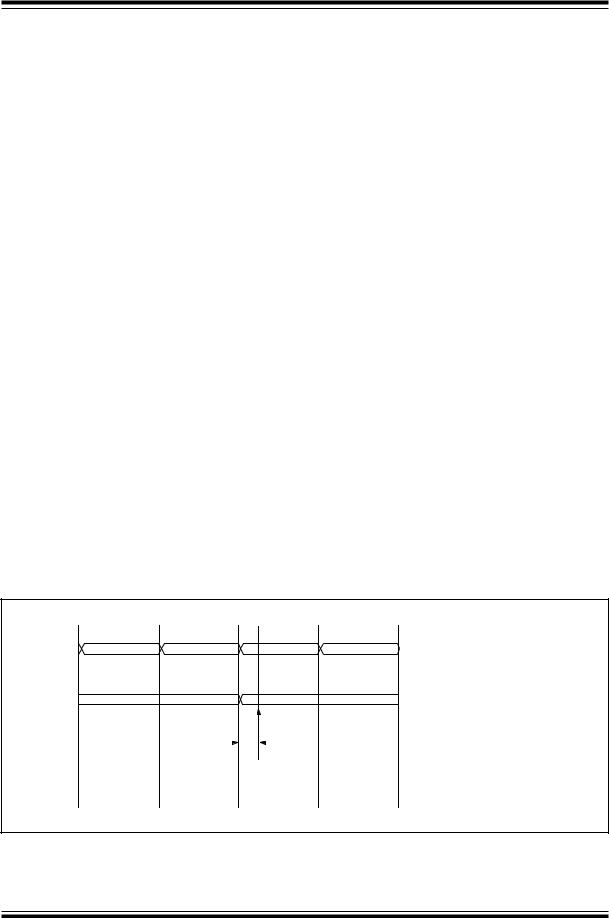
PIC16C84
5.3I/O Programming Considerations
5.3.1BI-DIRECTIONAL I/O PORTS
Any instruction which writes, operates internally as a read followed by a write operation. The BCF and BSF instructions, for example, read the register into the CPU, execute the bit operation and write the result back to the register. Caution must be used when these instructions are applied to a port with both inputs and outputs defined. For example, a BSF operation on bit5 of PORTB will cause all eight bits of PORTB to be read into the CPU. Then the BSF operation takes place on bit5 and PORTB is written to the output latches. If another bit of PORTB is used as a bi-directional I/O pin (i.e., bit0) and it is defined as an input at this time, the input signal present on the pin itself would be read into the CPU and rewritten to the data latch of this particular pin, overwriting the previous content. As long as the pin stays in the input mode, no problem occurs. However, if bit0 is switched into output mode later on, the content of the data latch is unknown.
Reading the port register, reads the values of the port pins. Writing to the port register writes the value to the port latch. When using read-modify-write instructions (i.e., BCF, BSF, etc.) on a port, the value of the port pins is read, the desired operation is done to this value, and this value is then written to the port latch.
A pin actively outputting a Low or High should not be driven from external devices at the same time in order to change the level on this pin (“wired-or”,“wired-and”). The resulting high output current may damage the chip.
5.3.2SUCCESSIVE OPERATIONS ON I/O PORTS
The actual write to an I/O port happens at the end of an instruction cycle, whereas for reading, the data must be valid at the beginning of the instruction cycle (Figure 5- 5). Therefore, care must be exercised if a write followed by a read operation is carried out on the same I/O port. The sequence of instructions should be such that the pin voltage stabilizes (load dependent) before the next instruction which causes that file to be read into the CPU is executed. Otherwise, the previous state of that pin may be read into the CPU rather than the new state. When in doubt, it is better to separate these instructions with a NOP or another instruction not accessing this I/O port.
Example 5-1 shows the effect of two sequential read- modify-write instructions (e.g., BCF, BSF, etc.) on an I/O port.
EXAMPLE 5-1: READ-MODIFY-WRITE INSTRUCTIONS ON AN I/O PORT
;Initial PORT settings: PORTB<7:4> Inputs ; PORTB<3:0> Outputs ;PORTB<7:6> have external pull-ups and are ;not connected to other circuitry
; |
|
|
; |
PORT latch |
PORT pins |
; |
---------- |
--------- |
BCF PORTB, 7 |
; 01pp ppp |
11pp ppp |
BCF PORTB, 6 |
; 10pp ppp |
11pp ppp |
BSF STATUS, RP0 |
; |
|
BCF TRISB, 7 |
; 10pp ppp |
11pp ppp |
BCF TRISB, 6 |
; 10pp ppp |
10pp ppp |
;
;Note that the user may have expected the ;pin values to be 00pp ppp. The 2nd BCF ;caused RB7 to be latched as the pin value ;(high).
FIGURE 5-5: SUCCESSIVE I/O OPERATION
|
Q1 |
Q2 |
|
Q3 |
Q4 |
Q1 |
Q2 |
Q3 |
Q4 |
Q1 |
Q2 |
Q3 |
Q4 |
Q1 |
Q2 |
Q3 |
Q4 |
||||
PC |
|
PC |
|
|
|
PC + 1 |
|
|
|
|
PC + 2 |
|
|
PC + 3 |
|
||||||
Instruction |
MOVWF PORTB |
MOVF PORTB,W |
|
|
|
|
|
|
|
|
|
|
|||||||||
fetched |
|
|
NOP |
|
|
NOP |
|
||||||||||||||
|
write to |
|
|
|
|
|
|
|
|
|
|
|
|
||||||||
|
|
|
|
|
|
|
|
|
|
|
|
|
|
||||||||
|
|
PORTB |
|
|
|
|
|
|
|
|
|
|
|
|
|
|
|
|
|
||
RB7:RB0 |
|
|
|
|
|
|
|
|
|
|
|
|
|
|
|
|
|
|
|
|
|
|
|
|
|
|
|
|
|
|
|
|
|
|
Port pin |
|
|
|
|
|
|||
|
|
|
|
|
|
|
|
|
|
|
|
|
|
|
|
|
|
||||
Instruction |
|
|
|
|
|
|
|
|
|
|
|
TPD |
sampled here |
|
NOP |
|
|||||
|
|
|
|
|
|
|
|
|
|
|
|
|
|
|
|
|
|
||||
|
|
|
|
|
|
|
|
|
|
|
|
|
|
|
|
|
|
||||
|
|
|
|
|
|
|
|
|
|
|
|
|
|
|
|
|
|
|
|||
executed |
|
|
|
|
|
|
|
|
|
|
|
|
|
|
|
|
|
|
|
||
|
|
|
|
|
MOVWF PORTB |
|
|
|
|
|
|
|
|
|
|
||||||
|
|
|
|
|
|
MOVF PORTB,W |
|
|
|
|
|||||||||||
|
|
|
|
|
|
|
write to |
|
|
|
|
|
|
|
|
|
|
|
|
||
|
|
|
|
|
|
|
PORTB |
|
|
|
|
|
|
|
|
|
|
|
|
||
Note:
This example shows a write to PORTB followed by a read from PORTB.
Note that:
data setup time = (0.25TCY - TPD)
where TCY = instruction cycle TPD = propagation delay
Therefore, at higher clock frequencies, a write followed by a read may be problematic.
1997 Microchip Technology Inc. |
DS30445C-page 23 |

PIC16C84
NOTES:
DS30445C-page 24 |
1997 Microchip Technology Inc. |
PIC16C84
6.0TIMER0 MODULE AND TMR0 REGISTER
The Timer0 module timer/counter has the following features:
•8-bit timer/counter
•Readable and writable
•8-bit software programmable prescaler
•Internal or external clock select
•Interrupt on overflow from FFh to 00h
•Edge select for external clock
Timer mode is selected by clearing the T0CS bit (OPTION<5>). In timer mode, the Timer0 module (Figure 6-1) will increment every instruction cycle (without prescaler). If the TMR0 register is written, the increment is inhibited for the following two cycles (Figure 6-2 and Figure 6-3). The user can work around this by writing an adjusted value to the TMR0 register.
Counter mode is selected by setting the T0CS bit (OPTION<5>). In this mode TMR0 will increment either on every rising or falling edge of pin RA4/T0CKI. The incrementing edge is determined by the T0 source
edge select bit, T0SE (OPTION<4>). Clearing bit T0SE selects the rising edge. Restrictions on the external clock input are discussed in detail in Section 6.2.
The prescaler is shared between the Timer0 Module and the Watchdog Timer. The prescaler assignment is controlled, in software, by control bit PSA (OPTION<3>). Clearing bit PSA will assign the prescaler to the Timer0 Module. The prescaler is not readable or writable. When the prescaler (Section 6.3) is assigned to the Timer0 Module, the prescale value (1:2, 1:4, ..., 1:256) is software selectable.
6.1TMR0 Interrupt
The TMR0 interrupt is generated when the TMR0 register overflows from FFh to 00h. This overflow sets the T0IF bit (INTCON<2>). The interrupt can be masked by clearing enable bit T0IE (INTCON<5>). The T0IF bit must be cleared in software by the Timer0 Module interrupt service routine before re-enabling this interrupt. The TMR0 interrupt (Figure 6-4) cannot wake the processor from SLEEP since the timer is shut off during SLEEP.
FIGURE 6-1: TMR0 BLOCK DIAGRAM
|
|
|
|
|
|
|
|
|
|
|
|
|
|
|
|
|
|
|
|
|
|
|
Data bus |
||||
|
|
|
FOSC/4 |
|
|
0 |
|
|
|
|
|
1 |
PSout |
|
|
|
|
8 |
|
|
|||||||
|
|
|
|
|
|
|
|
|
|
|
|
|
|
|
|
||||||||||||
|
|
|
|
|
|
|
|
|
|
|
|
|
|
|
|
|
|
|
|
|
|
||||||
|
|
|
|
|
|
|
|
|
|
|
|
|
|
|
|
|
|
Sync with |
|
|
|
|
|
|
|||
|
|
|
|
|
|
|
|
|
|
1 |
|
|
|
|
|
|
|
|
|
|
TMR0 register |
|
|
||||
|
|
|
|
|
|
|
|
|
|
|
|
|
|
|
|
|
|
Internal |
|
|
|
||||||
RA4/T0CKI |
|
|
|
|
|
|
|
|
|
|
|
Programmable |
|
0 |
|
clocks |
|
|
|
|
|
|
|||||
|
|
|
|
|
|
|
|
|
|
|
|
|
PSout |
|
|||||||||||||
|
|
|
|
|
|
|
|
|
|
|
|
|
|
|
|||||||||||||
|
pin |
|
|
|
|
|
|
|
|
|
|
Prescaler |
|
|
|
|
|
|
|
|
|
|
|
|
|||
|
|
|
|
|
|
|
|
|
|
|
|
|
|
|
|
(2 cycle delay) |
|
|
|
|
|
|
|||||
|
|
T0SE |
|
|
|
|
|
|
|
|
|
|
|
|
|
|
|
|
|
|
|
|
|||||
|
|
|
|
|
|
|
|
|
|
3 |
|
|
|
|
|
|
|
|
|
|
|
||||||
|
|
|
|
|
|
|
|
|
|
|
|
|
|
|
|
|
|
|
|
|
Set bit T0IF |
||||||
|
|
|
|
|
|
|
|
|
|
|
|
|
|
|
|
|
PSA |
|
|
|
|
||||||
|
|
|
|
|
|
|
|
|
|
|
|
|
|
PS2, PS1, PS0 |
|
|
|||||||||||
|
|
|
|
|
|
|
|
|
|
|
|
|
|
|
|
|
|
on Overflow |
|||||||||
|
|
|
|
|
|
|
|
|
|
|
|
|
|||||||||||||||
T0CS
Note 1: Bits T0CS, T0SE, PS2, PS1, PS0 and PSA are located in the OPTION register. 2: The prescaler is shared with the Watchdog Timer (Figure 6-6)
FIGURE 6-2: TMR0 TIMING: INTERNAL CLOCK/NO PRESCALER |
|
|
|
|
|
|
|
|
|
|
|
|||||||||||||||||||||
|
Q1 |
Q2 |
Q3 |
Q4 |
Q1 |
Q2 |
Q3 |
Q4 |
Q1 |
Q2 |
Q3 |
Q4 |
Q1 |
Q2 |
Q3 |
Q4 |
Q1 |
Q2 |
Q3 |
Q4 |
Q1 |
Q2 |
Q3 |
Q4 |
Q1 |
Q2 |
Q3 |
Q4 |
Q1 |
Q2 |
Q3 |
Q4 |
PC |
|
PC-1 |
|
|
PC |
|
|
|
PC+1 |
|
|
PC+2 |
|
|
PC+3 |
|
|
PC+4 |
|
|
PC+5 |
|
|
PC+6 |
|
|||||||
Instruction |
|
|
|
|
MOVWF TMR0 |
MOVF TMR0,W |
MOVF TMR0,W |
MOVF TMR0,W |
MOVF TMR0,W |
MOVF TMR0,W |
|
|
|
|
||||||||||||||||||
Fetch |
|
|
|
|
|
|
|
|
|
|
|
|
|
|
|
|
|
|
|
|
|
|
|
|
|
|
|
|
|
|
|
|
TMR0 |
T0 |
|
|
|
T0+1 |
|
|
T0+2 |
|
|
NT0 |
|
|
NT0 |
|
|
NT0 |
|
|
|
NT0+1 |
|
|
NT0+2 |
T0 |
|||||||
Instruction |
|
|
|
|
|
|
|
|
Write TMR0 |
Read TMR0 |
Read TMR0 |
Read TMR0 |
Read TMR0 |
Read TMR0 |
||||||||||||||||||
Executed |
|
|
|
|
|
|
|
|
||||||||||||||||||||||||
|
|
|
|
|
|
|
|
|
executed |
|
reads NT0 |
|
reads NT0 |
|
reads NT0 |
|
reads NT0 + 1 |
reads NT0 + 2 |
||||||||||||||
1997 Microchip Technology Inc. |
DS30445C-page 25 |
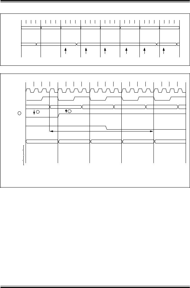
PIC16C84 |
|
|
|
|
|
|
|
|
|
|
|
|
|
|
|
|
|
|
|
|
|
|
|
|
|
|
|
|
||||
FIGURE 6-3: TMR0 TIMING: INTERNAL CLOCK/PRESCALE 1:2 |
|
|
|
|
|
|
|
|
|
|
|
|||||||||||||||||||||
|
Q1 |
Q2 |
Q3 |
Q4 |
Q1 |
Q2 |
Q3 |
Q4 |
Q1 |
Q2 |
Q3 |
Q4 |
Q1 |
Q2 |
Q3 |
Q4 |
Q1 |
Q2 |
Q3 |
Q4 |
Q1 |
Q2 |
Q3 |
Q4 |
Q1 |
Q2 |
Q3 |
Q4 |
Q1 |
Q2 |
Q3 |
Q4 |
PC |
|
PC-1 |
|
|
PC |
|
|
PC+1 |
|
|
PC+2 |
|
|
PC+3 |
|
|
PC+4 |
|
|
PC+5 |
|
|
PC+6 |
|
||||||||
Instruction |
|
|
|
|
MOVWF TMR0 |
MOVF TMR0,W |
MOVF TMR0,W |
MOVF TMR0,W |
MOVF TMR0,W |
MOVF TMR0,W |
|
|
|
|
||||||||||||||||||
Fetch |
|
|
|
|
|
|
|
|
|
|
|
|
|
|
|
|
|
|
|
|
|
|
|
|
|
|
|
|
|
|
|
|
TMR0 |
T0 |
|
|
|
|
|
T0+1 |
|
|
|
|
|
|
|
|
|
|
|
NT0 |
|
|
|
|
|
|
|
|
|
NT0+1 |
|
||
Instruction |
|
|
|
|
|
|
|
|
Write TMR0 |
Read TMR0 |
Read TMR0 |
Read TMR0 |
Read TMR0 |
Read TMR0 |
||||||||||||||||||
Execute |
|
|
|
|
|
|
|
|
||||||||||||||||||||||||
|
|
|
|
|
|
|
|
executed |
|
reads NT0 |
|
reads NT0 |
|
reads NT0 |
|
reads NT0 |
|
reads NT0 + 1 |
||||||||||||||
|
|
|
|
|
|
|
|
|
|
|
|
|
|
|||||||||||||||||||
FIGURE 6-4: |
TMR0 INTERRUPT TIMING |
|
|
|
|
|
|
|
|
|
|
|
|
|
|
|
|
|
|
|
|
|||||||||||
Q1 |
Q2 |
Q3 |
Q4 |
Q1 |
Q2 |
Q3 |
Q4 |
Q1 |
Q2 |
Q3 |
Q4 |
Q1 |
Q2 |
Q3 |
Q4 |
Q1 |
Q2 |
Q3 |
Q4 |
OSC1 |
|
|
|
|
|
|
|
|
|
|
|
|
|
|
|
|
|
|
|
CLKOUT(3) |
|
|
|
|
|
|
|
|
|
|
|
|
|
|
|
|
|
|
|
TMR0 timer |
FEh |
|
|
FFh |
|
|
00h |
|
|
01h |
|
|
|
02h |
|
|
|||
T0IF bit 4 |
1 |
|
|
|
1 |
|
|
|
|
|
|
|
|
|
|
|
|
|
|
|
|
|
|
|
|
|
|
|
|
|
|
|
|
|
|
|
|
|
|
(INTCON<2>) |
|
|
|
|
|
|
|
|
|
|
|
|
|
|
|
|
|
|
|
GIE bit |
|
|
|
|
|
|
|
|
|
|
|
|
|
|
|
|
|
|
|
(INTCON<7>) |
|
|
|
|
|
|
|
|
|
|
|
|
|
|
|
|
|
|
|
INSTRUCTION FLOW |
|
|
|
|
|
|
|
Interrupt Latency(2) |
|
|
|
|
|
|
|
|
|||
|
|
|
|
|
|
|
|
|
|
|
|
|
|
|
|
|
|
|
|
PC |
PC |
|
|
|
PC +1 |
|
|
PC +1 |
|
|
0004h |
|
|
0005h |
|
||||
Instruction |
Inst (PC) |
|
|
Inst (PC+1) |
|
|
|
|
|
|
Inst (0004h) |
|
|
Inst (0005h) |
|
||||
fetched |
|
|
|
|
|
|
|
|
|
|
|
||||||||
|
|
|
|
|
|
|
|
|
|
|
|
|
|
|
|
|
|
|
|
Instruction |
Inst (PC-1) |
|
|
Inst (PC) |
|
|
Dummy cycle |
|
|
Dummy cycle |
|
|
Inst (0004h) |
|
|||||
executed |
|
|
|
|
|
|
|
|
|
||||||||||
|
|
|
|
|
|
|
|
|
|
|
|
|
|
|
|
|
|
|
|
Note 1: T0IF interrupt flag is sampled here (every Q1).
2:Interrupt latency = 3.25Tcy, where Tcy = instruction cycle time.
3:CLKOUT is available only in RC oscillator mode.
4:The timer clock (after the synchronizer circuit) which increments the timer from FFh to 00h immediately sets the T0IF bit. The TMR0 register will roll over 3 Tosc cycles later.
DS30445C-page 26 |
1997 Microchip Technology Inc. |
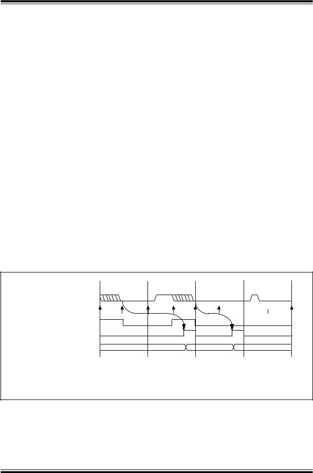
PIC16C84
6.2Using TMR0 with External Clock
When an external clock input is used for TMR0, it must meet certain requirements. The external clock requirement is due to internal phase clock (TOSC) synchronization. Also, there is a delay in the actual incrementing of the TMR0 register after synchronization.
6.2.1EXTERNAL CLOCK SYNCHRONIZATION
When no prescaler is used, the external clock input is the same as the prescaler output. The synchronization of pin RA4/T0CKI with the internal phase clocks is accomplished by sampling the prescaler output on the Q2 and Q4 cycles of the internal phase clocks (Figure 6-5). Therefore, it is necessary for T0CKI to be high for at least 2Tosc (plus a small RC delay) and low for at least 2Tosc (plus a small RC delay). Refer to the electrical specification of the desired device.
When a prescaler is used, the external clock input is divided by an asynchronous ripple counter type prescaler so that the prescaler output is symmetrical. For the external clock to meet the sampling requirement, the ripple counter must be taken into account. Therefore, it is necessary for T0CKI to have a period of at least 4Tosc (plus a small RC delay) divided by the prescaler value. The only requirement on T0CKI high and low time is that they do not violate the minimum pulse width requirement of 10 ns. Refer to parameters 40, 41 and 42 in the AC Electrical Specifications of the desired device.
6.2.2TMR0 INCREMENT DELAY
Since the prescaler output is synchronized with the internal clocks, there is a small delay from the time the external clock edge occurs to the time the Timer0 Module is actually incremented. Figure 6-5 shows the delay from the external clock edge to the timer incrementing.
6.3Prescaler
An 8-bit counter is available as a prescaler for the Timer0 Module, or as a postscaler for the Watchdog Timer (Figure 6-6). For simplicity, this counter is being referred to as “prescaler”throughout this data sheet. Note that there is only one prescaler available which is mutually exclusive between the Timer0 Module and the Watchdog Timer. Thus, a prescaler assignment for the Timer0 Module means that there is no prescaler for the Watchdog Timer, and vice-versa.
The PSA and PS2:PS0 bits (OPTION<3:0>) determine the prescaler assignment and prescale ratio.
When assigned to the Timer0 Module, all instructions writing to the Timer0 Module (e.g., CLRF 1, MOVWF 1, BSF 1,x ....etc.) will clear the prescaler. When assigned to WDT, a CLRWDT instruction will clear the prescaler along with the Watchdog Timer. The prescaler is not readable or writable.
FIGURE 6-5: TIMER0 TIMING WITH EXTERNAL CLOCK
Q1 |
Q2 |
Q3 |
Q4 |
Q1 |
Q2 |
Q3 |
Q4 |
Q1 |
Q2 |
Q3 |
Q4 |
Q1 |
Q2 |
Q3 |
Q4 |
Ext. Clock Input or
Prescaler Out (Note 2)
 (Note 3)
Ext. Clock/Prescaler
Output After Sampling
Increment TMR0 (Q4)
TMR0 |
T0 |
T0 + 1 |
T0 + 2 |
Note 1: Delay from clock input change to TMR0 increment is 3Tosc to 7Tosc. (Duration of Q = Tosc). Therefore, the error in measuring the interval between two edges on TMR0 input = ± 4Tosc max.
2:External clock if no prescaler selected, Prescaler output otherwise.
3:The arrows ↑ indicate where sampling occurs. A small clock pulse may be missed by sampling.
1997 Microchip Technology Inc. |
DS30445C-page 27 |
PIC16C84
FIGURE 6-6: BLOCK DIAGRAM OF THE TMR0/WDT PRESCALER
CLKOUT (= Fosc/4) |
|
|
|
|
|
|
|
|
|
|
|
|
|
|
|
|
|
|
|
|
|
|
|
|
|
|
|
|
|
|
|
|
|
|
Data Bus |
|||||||||||
|
|
|
|
|
|
|
|
|
|
|
|
|
|
|
|
|
|
|
|
|
|
|
|
|
|
|
|
|
|
|
|
|
|
|||||||||||||
|
|
|
|
|
|
|
|
|
|
|
|
|
|
|
|
|
|
|
|
|
|
|
|
|
|
|
|
|
|
|
|
|
|
|
|
|
|
|
|
|
|
8 |
|
|
||
|
|
|
|
|
|
|
|
|
|
|
|
|
|
|
|
|
|
|
M |
|
|
1 |
|
|
|
|
|
|
|
|
|
|
|
|
|
|
|
|||||||||
|
|
|
|
|
|
|
|
|
|
|
|
|
|
|
|
|
0 |
|
|
|
|
|
|
|
|
|
|
|
|
|
|
|
|
|
||||||||||||
|
|
|
|
|
|
|
|
|
|
|
|
|
|
|
|
|
|
|
|
|
|
|
|
|
|
|
|
|
|
|
|
|
|
|||||||||||||
RA4/T0CKI |
|
|
|
|
|
|
|
|
|
|
|
|
|
|
|
|
|
U |
|
|
|
|
|
|
|
M |
|
|
|
|
|
|
SYNC |
|
|
|
|
|
|
|
||||||
|
|
|
|
|
|
|
|
|
|
|
|
|
|
|
|
|
|
|
|
|
|
|
|
|
|
|
|
|
|
|
|
|
|
|
|
|||||||||||
pin |
|
|
|
|
|
|
|
|
|
|
|
|
|
|
|
|
|
X |
|
|
|
|
|
|
|
U |
|
|
|
|
|
|
|
|
|
TMR0 register |
|
|
||||||||
|
|
|
|
|
|
|
|
|
|
|
|
|
|
|
|
|
|
|
|
|
|
|
|
|
|
|
|
|
||||||||||||||||||
|
|
|
|
|
|
|
|
|
|
|
|
|
|
|
|
|
|
|
0 |
|
|
|
|
|
|
|
|
2 |
|
|
|
|
|
|||||||||||||
|
|
|
|
|
|
|
|
|
|
|
|
|
|
1 |
|
|
|
|
|
|
|
|
|
|
|
|
|
|
|
|
|
|||||||||||||||
|
|
|
|
|
|
|
|
|
|
|
|
|
|
|
|
|
|
|
|
|
|
|
|
|
|
X |
|
|
|
|
|
|
Cycles |
|
|
|
|
|
|
|
||||||
|
|
|
|
|
|
|
|
|
|
|
|
|
|
|
|
|
|
|
|
|
|
|
|
|
|
|
|
|
|
|
|
|
|
|
|
|
|
|
|
|
|
|
||||
|
|
|
|
|
|
|
|
|
|
|
|
|
|
|
|
|
|
|
|
|
|
|
|
|
|
|
|
|
|
|
|
|
|
|
|
|
|
|
|
|
|
|||||
|
|
|
|
|
|
|
|
|
|
|
|
|
|
|
|
|
|
|
|
|
|
|
|
|
|
|
|
|
|
|
|
|
|
|
|
|
|
|
|
|
|
|
|
|
|
|
|
|
|
|
|
|
T0SE |
|
|
|
|
|
|
|
|
|
|
|
|
|
|
|
|
|
|
|
|
|
|
|
|
|
|
|
|
|
|
|
|
|
|
|
|
|
|||
|
|
|
|
|
|
|
|
|
|
|
|
|
|
|
|
|
|
T0CS |
|
|
|
|
|
|
|
|
|
|
|
|
|
|
|
|
|
|
|
|
Set bit T0IF |
|||||||
|
|
|
|
|
|
|
|
|
|
|
|
|
|
|
|
|
|
|
|
|
|
PSA |
|
|
|
|
|
|
|
|
|
|
|
|
|
|||||||||||
|
|
|
|
|
|
|
|
|
|
|
|
|
|
|
|
|
|
|
|
|
|
|
|
|
|
|
|
|
|
|
|
|
|
|
|
|
|
|
|
|
|
|||||
|
|
|
|
|
|
|
|
|
|
|
|
|
|
|
|
|
|
|
|
|
|
|
|
|
|
|
|
|
|
|
|
|
|
|
|
|
|
|
|
|
|
|
|
|
on overflow |
|
|
|
|
|
|
|
|
|
|
|
0 |
|
|
|
|
|
|
|
|
|
|
|
|
|
|
|
|
|
|
|
|
|
|
|
|
|
|
|
|
|
|
|
|
|
|
|
|
|
|
|
|
|
|
|
|
|
|
|
|
M |
|
|
|
|
|
|
8-bit Prescaler |
|
|
|
|
|
|
|
|
|
|
|
|
|
|
|
||||||||||||
|
|
|
|
|
|
|
|
|
|
|
|
|
|
|
|
|
|
|
|
|
|
|
|
|
|
|
|
|
|
|
|
|
|
|
||||||||||||
|
|
|
|
|
|
|
|
|
|
|
|
|
|
|
|
|
|
|
|
|
|
|
|
|
|
|
|
|
|
|
|
|
|
|
|
|
|
|
|
|
|
|
|
|||
|
|
|
|
|
|
|
|
|
|
1 |
|
|
U |
|
|
|
|
|
|
|
|
|
|
|
|
|
|
|
|
|
|
|
|
|
|
|
|
|
|
|
|
|
|
|||
|
Watchdog |
|
|
|
|
|
|
|
X |
|
|
|
|
|
|
|
|
8 |
|
|
|
|
|
|
|
|
|
|
|
|
|
|
|
|
|
|
|
|
|
|||||||
|
|
|
|
|
|
|
|
|
|
|
|
|
|
|
|
|
|
|
|
|
|
|
|
|
|
|
|
|
|
|
|
|
|
|
|
|
|
|
|
|||||||
|
Timer |
|
|
|
|
|
|
|
|
|
|
|
|
|
|
|
|
|
|
|
|
|
|
|
|
|
|
|
|
|
|
|
|
|
|
|
|
|
|
|
|
|
||||
|
|
|
|
|
|
|
|
|
|
|
|
|
|
|
|
|
|
|
|
|
|
|
|
|
|
|
|
|
|
|
|
|
|
|
|
|
|
|
|
|
|
|
|
|||
|
|
|
|
|
|
|
|
|
|
|
|
|
|
|
|
|
|
|
|
|
|
|
|
|
|
|
|
|
|
|
|
|
|
|
|
|
|
|
|
|
|
|
|
|
|
|
|
|
|
|
|
|
|
|
|
|
|
|
|
|
|
|
|
|
|
|
|
|
|
|
8 - to - 1MUX |
|
|
|
|
|
|
|
|
PS2:PS0 |
|
|
|
|
|
|
|
||||||
|
|
|
|
|
|
|
|
|
|
|
|
|
|
|
|
|
|
|
|
|
|
|
|
|
|
|
|
|
|
|
|
|
|
|
|
|
|
|
||||||||
|
|
|
|
|
|
|
|
|
|
|
|
|
|
|
|
|
|
|
|
|
|
|
|
|
|
|
|
|
|
|
|
|
|
|
|
|
|
|||||||||
|
|
|
|
|
|
|
|
|
|
|
|
|
PSA |
|
|
|
|
|
|
|
|
|
|
|
|
|
|
|
|
|
|
|
|
|
|
|
|
|
|
|
|
|
|
|||
|
|
|
|
|
|
|
|
|
|
|
|
|
|
|
|
|
|
|
|
|
|
|
|
|
|
|
|
|
|
|
|
|
|
|
|
|
|
|
|
|
|
|
||||
|
|
|
|
|
|
|
|
|
|
|
|
|
|
|
|
|
|
0 |
|
1 |
|
|
|
|
|
|
|
|
|
|
|
|
|
|
|
|
|
|
|
|||||||
WDT Enable bit |
|
|
|
|
|
|
|
|
|
|
|
|
|
|
|
|
|
|
|
|
|
|
|
|
|
|
|
|
||||||||||||||||||
|
|
|
|
|
|
|
|
|
|
|
|
|
|
|
M U X |
|
|
|
|
|
|
|
PSA |
|
|
|
|
|
|
|
||||||||||||||||
|
|
|
|
|
|
|
|
|
|
|
|
|
|
|
|
|
|
|
|
|
|
|
|
|
|
|
|
|
|
|
|
|
|
|
|
|
|
|
||||||||
|
|
|
|
|
|
|
|
|
|
|
|
|
|
|
|
|
|
|
|
|
|
|
|
|
|
|
|
|
|
|
|
|
|
|
|
|
|
|
||||||||
|
|
|
|
|
|
|
|
|
|
|
|
|
|
|
|
|
|
|
|
|
|
|
|
|
|
|
|
|
|
|
|
|
|
|
|
|
|
|
|
|
|
|
|
|
|
|
|
|
|
|
|
|
|
|
|
|
|
|
|
|
|
|
|
|
|
|
|
|
|
|
|
|
|
|
|
|
|
|
|
|
|
|
|
|
|
|
|
|
|
|
|
|
|
WDT time-out
Note: T0CS, T0SE, PSA, PS2:PS0 are bits in the OPTION register.
DS30445C-page 28 |
1997 Microchip Technology Inc. |

PIC16C84
6.3.1SWITCHING PRESCALER ASSIGNMENT
The prescaler assignment is fully under software control (i.e., it can be changed “on the y”fl during program execution).
Note: To avoid an unintended device RESET, the following instruction sequence (Example 6-1) must be executed when changing the prescaler assignment from Timer0 to the WDT. This sequence must be taken even if the WDT is disabled. To change prescaler from the WDT to the Timer0 module use the sequence shown in Example 6-2.
EXAMPLE 6-1: CHANGING PRESCALER (TIMER0→WDT)
BCF |
STATUS, RP0 |
;Bank 0 |
CLRF |
TMR0 |
;Clear TMR0 |
|
|
; and Prescaler |
BSF |
STATUS, RP0 |
;Bank 1 |
CLRWDT |
|
;Clears WDT |
MOVLW |
b'xxxx1xxx' |
;Select new |
MOVWF |
OPTION |
; prescale value |
BCF |
STATUS, RP0 |
;Bank 0 |
EXAMPLE 6-2: CHANGING PRESCALER (WDT→TIMER0)
CLRWDT |
|
;Clear WDT and |
|
|
; prescaler |
BSF |
STATUS, RP0 |
;Bank 1 |
MOVLW |
b'xxxx0xxx' |
;Select TMR0, new |
|
|
; prescale value |
|
|
’ and clock source |
MOVWF |
OPTION |
; |
BCF |
STATUS, RP0 |
;Bank 0 |
TABLE 6-1 |
REGISTERS ASSOCIATED WITH TIMER0 |
|
|
|
|
|
|
|
||||||||
|
|
|
|
|
|
|
|
|
|
|
|
|
|
|
|
|
|
|
|
|
|
|
|
|
|
|
|
|
|
Value on |
Value on all |
||
Address |
Name |
|
|
Bit 7 |
Bit 6 |
Bit 5 |
Bit 4 |
Bit 3 |
Bit 2 |
Bit 1 |
Bit 0 |
Power-on |
||||
|
|
other resets |
||||||||||||||
|
|
|
|
|
|
|
|
|
|
|
|
|
Reset |
|||
|
|
|
|
|
|
|
|
|
|
|
|
|
|
|
||
|
|
|
|
|
|
|
|
|
|
|
|
|
|
|
||
|
|
|
|
|
|
|
|
|
|
|
|
|
|
|||
01h |
TMR0 |
|
|
|
|
|
|
Timer0 module’s register |
|
|
|
xxxx xxxx |
uuuu uuuu |
|||
|
|
|
|
|
|
|
|
|
|
|
|
|
|
|
|
|
0Bh |
INTCON |
|
|
GIE |
EEIE |
T0IE |
INTE |
RBIE |
T0IF |
INTF |
RBIF |
0000 |
000x |
0000 |
0000 |
|
81h |
OPTION |
|
|
|
|
INTEDG |
T0CS |
T0SE |
PSA |
PS2 |
PS1 |
PS0 |
1111 |
1111 |
1111 |
1111 |
|
RBPU |
|||||||||||||||
85h |
TRISA |
|
|
— |
— |
— |
TRISA4 |
TRISA3 |
TRISA2 |
TRISA1 |
TRISA0 |
---1 |
1111 |
---1 |
1111 |
|
|
|
|
|
|
|
|
|
|
|
|
|
|
|
|
|
|
Legend: x = unknown, u = unchanged. - = unimplemented read as '0'Shaded. cells are not associated with Timer0.
1997 Microchip Technology Inc. |
DS30445C-page 29 |

PIC16C84
NOTES:
DS30445C-page 30 |
1997 Microchip Technology Inc. |
 Loading...