


 Loading...
Microchip Technology Inc PIC16F628-20I-SO, PIC16F627-04-P, PIC16F627-04I-SO, PIC16F627-04I-SS, PIC16F627-20I-P Datasheet
...PIC16F62X
FLASH-Based 8-Bit CMOS Microcontrollers
Devices included in this data sheet:
• PIC16F627 |
• PIC16F628 |
Referred to collectively as PIC16F62X .
High Performance RISC CPU:
•Only 35 instructions to learn
•All single-cycle instructions (200 ns), except for program branches which are two-cycle
•Operating speed:
-DC - 20 MHz clock input
-DC - 200 ns instruction cycle
|
|
Memory |
|
Device |
|
|
|
FLASH |
RAM |
EEPROM |
|
|
Program |
Data |
Data |
|
|
|
|
|
|
|
|
PIC16F627 |
1024 x 14 |
224 x 8 |
128 x 8 |
|
|
|
|
PIC16F628 |
2048 x 14 |
224 x 8 |
128 x 8 |
|
|
|
|
•Interrupt capability
•16 special function hardware registers
•8-level deep hardware stack
•Direct, Indirect and Relative addressing modes
Peripheral Features:
•15 I/O pins with individual direction control
•High current sink/source for direct LED drive
•Analog comparator module with:
-Two analog comparators
-Programmable on-chip voltage reference (VREF) module
-Programmable input multiplexing from device inputs and internal voltage reference
-Comparator outputs are externally accessible
•Timer0: 8-bit timer/counter with 8-bit programmable prescaler
•Timer1: 16-bit timer/counter with external crystal/ clock capability
•Timer2: 8-bit timer/counter with 8-bit period register, prescaler and postscaler
•Capture, Compare, PWM (CCP) module
-Capture is 16-bit, max. resolution is 12.5 ns
-Compare is 16-bit, max. resolution is 200 ns
-PWM max. resolution is 10-bit
•Universal Synchronous/Asynchronous Receiver/ Transmitter USART/SCI
•16 Bytes of common RAM
Special Microcontroller Features:
•Power-on Reset (POR)
•Power-up Timer (PWRT) and Oscillator Start-up Timer (OST)
•Brown-out Detect (BOD)
•Watchdog Timer (WDT) with its own on-chip RC oscillator for reliable operation
•Multiplexed MCLR-pin
•Programmable weak pull-ups on PORTB
•Programmable code protection
•Low voltage programming
•Power saving SLEEP mode
•Selectable oscillator options
-FLASH configuration bits for oscillator options
-ER (External Resistor) oscillator
-Reduced part count
-Dual speed INTRC
-Lower current consumption
-EC External Clock input
-XT oscillator mode
-HS oscillator mode
-LP oscillator mode
•Serial in-circuit programming (via two pins)
•Four user programmable ID locations
CMOS Technology:
•Low-power, high-speed CMOS FLASH technology
•Fully static design
•Wide operating voltage range
-PIC16F627 - 3.0V to 5.5V
-PIC16F628 - 3.0V to 5.5V
-PIC16LF627 - 2.0V to 5.5V
-PIC16LF628 - 2.0V to 5.5V
•Commercial, industrial and extended temperature range
•Low power consumption
-< 2.0 mA @ 5.0V, 4.0 MHz
-15 μA typical @ 3.0V, 32 kHz
-< 1.0 μA typical standby current @ 3.0V
© 1999 Microchip Technology Inc.
Preliminary
DS40300B-page 1
PIC16F62X
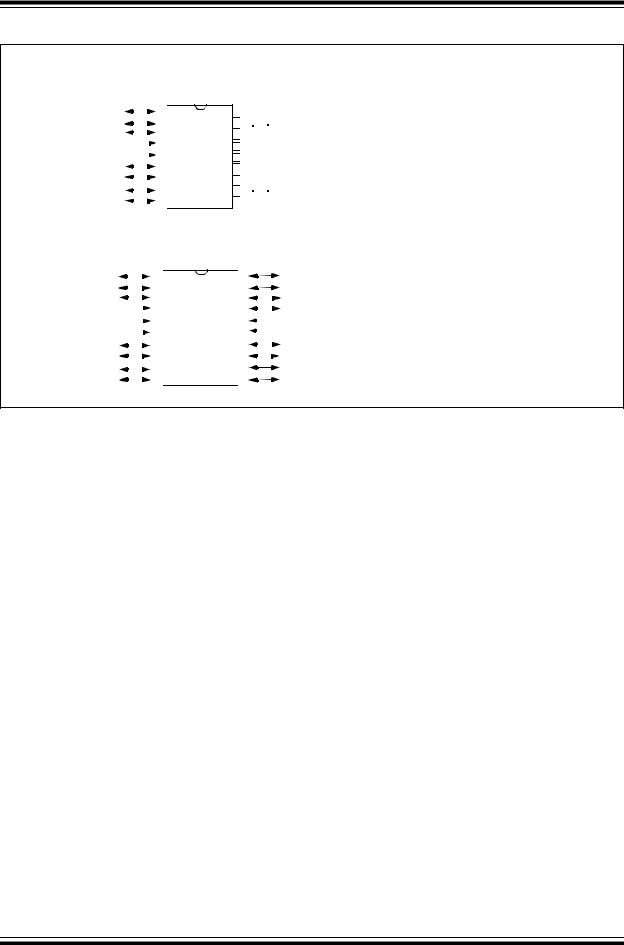
Pin Diagrams
PDIP, SOIC
RA2/AN2/VREF |
|
|
|
|
•1 |
||||
RA3/AN3/CMP1 |
|
|
|
|
|
||||
|
|
|
2 |
||||||
RA4/TOCKI/CMP2 |
|
|
|
3 |
|||||
|
|
|
|
|
|
|
|||
RA5/MCLR/THV |
|
|
|
4 |
|||||
|
|
||||||||
|
|
VSS |
|
|
|
5 |
|||
|
|
||||||||
|
RB0/INT |
|
|
|
6 |
||||
RB1/RX/DT |
|
|
|
7 |
|||||
RB2/TX/CK |
|
8 |
|||||||
|
RB3/CCP1 |
|
|
|
9 |
||||
|
|
|
|
|
|
|
|
|
|
PIC16F62X
18 

 RA1/AN1
17 

 RA0/AN0
16 

 RA7/OSC1/CLKIN 15


 RA6/OSC2/CLKOUT 14

 VDD
VDD
13 

 RB7/T1OSI
12 

 RB6/T1OSO/T1CKI 11

 RB5
RB5
10 

 RB4/PGM
SSOP
RA2/AN2/VREF |
|
|
|
|
•1 |
||||
RA3/AN3/CMP1 |
|
|
|
2 |
|||||
RA4/TOCKI/CMP2 |
|
|
|
3 |
|||||
|
|
|
|
|
|
|
|
||
RA5/MCLR/THV |
|
|
|
|
4 |
||||
|
|
|
|||||||
|
|
VSS |
|
|
|
|
|
|
5 |
|
|
VSS |
|
|
|
6 |
|||
|
RB0/INT |
|
|
|
|
7 |
|||
|
|
|
|
||||||
|
|
||||||||
|
|||||||||
RB1/RX/DT |
|
|
|
8 |
|||||
|
|||||||||
RB2/TX/CK |
|
|
|
9 |
|||||
|
|
||||||||
|
|||||||||
|
RB3/CCP1 |
|
|
|
10 |
||||
|
|
||||||||
PIC16F62X
20 |
|
|
|
|
|
|
RA1/AN1 |
|
|||||||
19 |
|
|
|
|
|
|
RA0/AN0 |
|
|||||||
18 |
|
|
|
|
|
|
RA7/OSC1/CLKIN |
17 |
|
|
|
|
|
|
RA6/OSC2/CLKOUT |
16 |
|
|
|
|
|
|
VDD |
15 |
|
|
|
|
|
|
VDD |
|
|
|
|
|
|
||
14 |
|
|
|
|
|
|
RB7/T1OSI |
13 |
|
|
|
|
|
|
RB6/T1OSO/T1CKI |
12 |
|
|
|
|
|
|
RB5 |
|
|
||||||
11 |
|
|
|
|
|
|
RB4/PGM |
|
Device Differences
|
Voltage |
|
Process |
|
Device |
Oscillator |
Technology |
||
Range |
||||
|
|
(Microns) |
||
|
|
|
||
|
|
|
|
|
|
|
|
|
|
PIC16F627 |
3.0 - 5.5 |
See Note 1 |
0.7 |
|
|
|
|
|
|
PIC16F628 |
3.0 - 5.5 |
See Note 1 |
0.7 |
|
|
|
|
|
|
PIC16LF627 |
2.0 - 5.5 |
See Note 1 |
0.7 |
|
|
|
|
|
|
PIC16LF628 |
2.0 - 5.5 |
See Note 1 |
0.7 |
|
|
|
|
|
Note 1: If you change from this device to another device, please verify oscillator characteristics in your application.
DS40300B-page 2 |
Preliminary |
© 1999 Microchip Technology Inc. |

|
|
PIC16F62X |
Table of Contents |
|
|
1.0 |
General Description ..................................................................................................................................................................... |
5 |
2.0 |
PIC16F62X Device Varieties ...................................................................................................................................................... |
7 |
3.0 |
Architectural Overview ................................................................................................................................................................ |
9 |
4.0 |
Memory Organization ................................................................................................................................................................ |
13 |
5.0 |
I/O Ports .................................................................................................................................................................................... |
27 |
6.0 |
Timer0 Module .......................................................................................................................................................................... |
45 |
7.0 |
Timer1 Module .......................................................................................................................................................................... |
50 |
8.0 |
Timer2 Module .......................................................................................................................................................................... |
54 |
9.0 |
Comparator Module ................................................................................................................................................................... |
57 |
10.0 |
Capture/Compare/PWM (CCP) Module .................................................................................................................................... |
63 |
11.0 |
Voltage Reference Module ........................................................................................................................................................ |
69 |
12.0 |
Universal Synchronous Asynchronous Receiver Transmitter (USART) .................................................................................... |
71 |
13.0 |
Data EEPROM Memory ............................................................................................................................................................ |
91 |
14.0 |
Special Features of the CPU ..................................................................................................................................................... |
95 |
15.0 |
Instruction Set Summary ......................................................................................................................................................... |
113 |
16.0 |
Development Support .............................................................................................................................................................. |
125 |
17.0 |
Electrical Specifications ........................................................................................................................................................... |
131 |
18.0 |
Device Characterization Information ....................................................................................................................................... |
145 |
19.0 |
Packaging Information ............................................................................................................................................................. |
147 |
Index |
.................................................................................................................................................................................................. |
151 |
On-Line .................................................................................................................................................................................Support |
155 |
|
Reader ..............................................................................................................................................................................Response |
156 |
|
PIC16F62X ........................................................................................................................................Product Identification System |
157 |
|
To Our Valued Customers
Most Current Data Sheet
To obtain the most up-to-date version of this data sheet, please register at our Worldwide Web site at:
http://www.microchip.com
You can determine the version of a data sheet by examining its literature number found on the bottom outside corner of any page. The last character of the literature number is the version number. e.g., DS30000A is version A of document DS30000.
New Customer Notification System
Register on our web site (www.microchip.com/cn) to receive the most current information on our products.
Errata
An errata sheet may exist for current devices, describing minor operational differences (from the data sheet) and recommended workarounds. As device/documentation issues become known to us, we will publish an errata sheet. The errata will specify the revision of silicon and revision of document to which it applies.
To determine if an errata sheet exists for a particular device, please check with one of the following:
•Microchip’s Worldwide Web site; http://www.microchip.com
•Your local Microchip sales office (see last page)
•The Microchip Corporate Literature Center; U.S. FAX: (602) 786-7277
When contacting a sales office or the literature center, please specify which device, revision of silicon and data sheet (include literature number) you are using.
Corrections to this Data Sheet
We constantly strive to improve the quality of all our products and documentation. We have spent a great deal of time to ensure that this document is correct. However, we realize that we may have missed a few things. If you find any information that is missing or appears in error, please:
•Fill out and mail in the reader response form in the back of this data sheet.
•E-mail us at webmaster@microchip.com.
We appreciate your assistance in making this a better document.
© 1999 Microchip Technology Inc. |
Preliminary |
DS40300B-page 3

PIC16F62X
NOTES:
DS40300B-page 4 |
Preliminary |
© 1999 Microchip Technology Inc. |

PIC16F62X
1.0GENERAL DESCRIPTION
The PIC16F62X are 18-Pin FLASH-based members of the versatile PIC16CXX family of low-cost, high-performance, CMOS, fully-static, 8-bit microcontrollers.
All PICmicro® microcontrollers employ an advanced RISC architecture. The PIC16F62X have enhanced core features, eight-level deep stack, and multiple internal and external interrupt sources. The separate instruction and data buses of the Harvard architecture allow a 14-bit wide instruction word with the separate 8-bit wide data. The two-stage instruction pipeline allows all instructions to execute in a single-cycle, except for program branches (which require two cycles). A total of 35 instructions (reduced instruction set) are available. Additionally, a large register set gives some of the architectural innovations used to achieve a very high performance.
PIC16F62X microcontrollers typically achieve a 2:1 code compression and a 4:1 speed improvement over other 8-bit microcontrollers in their class.
PIC16F62X devices have special features to reduce external components, thus reducing system cost, enhancing system reliability and reducing power consumption. There are eight oscillator configurations, of which the single pin ER oscillator provides a low-cost solution. The LP oscillator minimizes power consumption, XT is a standard crystal, INTRC is a self-contained internal oscillator and the HS is for High Speed crystals. The SLEEP (power-down) mode offers power savings. The user can wake up the chip from SLEEP through several external and internal interrupts and reset.
A highly reliable Watchdog Timer with its own on-chip RC oscillator provides protection against software lockup.
Table 1-1 shows the features of the PIC16F62X mid-range microcontroller families.
A simplified block diagram of the PIC16F62X is shown in Figure 3-1.
The PIC16F62X series fits in applications ranging from battery chargers to low-power remote sensors. The FLASH technology makes customization of application programs (detection levels, pulse generation, timers, etc.) extremely fast and convenient. The small footprint packages make this microcontroller series ideal for all applications with space limitations. Low-cost, low-power, high-performance, ease of use and I/O flexibility make the PIC16F62X very versatile.
1.1Development Support
The PIC16F62X family is supported by a full-featured macro assembler, a software simulator, an in-circuit emulator, a low-cost development programmer and a full-featured programmer. A Third Party “C” compiler support tool is also available.
© 1999 Microchip Technology Inc.
Preliminary
DS40300B-page 5

PIC16F62X
TABLE 1-1: |
PIC16F62X FAMILY OF DEVICES |
|
|
|
|
|
|
|
|
|
|
|
|
|
|
|
|
|
|
PIC16F627 |
|
PIC16F628 |
|
PIC16LF627 |
|
PIC16LF628 |
|
|
|
|
|
|
|
|
|
Clock |
Maximum Frequency |
20 |
|
20 |
|
20 |
|
20 |
of Operation (MHz) |
|
|
|
|
|
|
|
|
|
|
|
|
|
|
|
|
|
|
FLASH Program Memory (words) |
1024 |
|
2048 |
|
1024 |
|
2048 |
Memory |
|
|
|
|
|
|
|
|
RAM Data Memory (bytes) |
224 |
|
224 |
|
224 |
|
224 |
|
|
|
|
|
|
|
|
|
|
|
EEPROM Data Memory (bytes) |
128 |
|
128 |
|
128 |
|
128 |
|
Timer Module(s) |
TMR0, TMR1, TMR2 |
|
TMR0, TMR1, TMR2 |
|
TMR0, TMR1, TMR2 |
|
TMR0, TMR1, TMR2 |
|
|
|
|
|
|
|
|
|
|
Comparators(s) |
2 |
|
2 |
|
2 |
|
2 |
Peripherals |
|
|
|
|
|
|
|
|
Capture/Compare/PWM modules |
1 |
|
1 |
|
1 |
|
1 |
|
|
|
|
|
|
|
|
|
|
|
Serial Communications |
USART |
|
USART |
|
USART |
|
USART |
|
|
|
|
|
|
|
|
|
|
Internal Voltage Reference |
Yes |
|
Yes |
|
Yes |
|
Yes |
|
Interrupt Sources |
10 |
|
10 |
|
10 |
|
10 |
|
|
|
|
|
|
|
|
|
|
I/O Pins |
16 |
|
16 |
|
16 |
|
16 |
|
|
|
|
|
|
|
|
|
Features |
Voltage Range (Volts) |
3.0-5.5 |
|
3.0-5.5 |
|
2.0-5.5 |
|
2.0-5.5 |
|
|
|
|
|
|
|
|
|
Brown-out Detect |
Yes |
|
Yes |
|
Yes |
|
Yes |
|
|
|
|
|
|||||
|
|
|
|
|
|
|
|
|
|
Packages |
18-pin DIP, |
|
18-pin DIP, |
|
18-pin DIP, |
|
18-pin DIP, |
|
|
SOIC; |
|
SOIC; |
|
SOIC; |
|
SOIC; |
|
|
20-pin SSOP |
|
20-pin SSOP |
|
20-pin SSOP |
|
20-pin SSOP |
|
|
|
|
|
|
|
|
|
All PICmicro®Family devices have Power-on Reset, selectable Watchdog Timer, selectable code protect and high I/O current capability. All PIC16F62X Family devices use serial programming with clock pin RB6 and data pin RB7.
DS40300B-page 6 |
Preliminary |
© 1999 Microchip Technology Inc. |

PIC16F62X
2.0PIC16F62X DEVICE VARIETIES
A variety of frequency ranges and packaging options are available. Depending on application and production requirements the proper device option can be selected using the information in the PIC16F62X Product Identification System section at the end of this data sheet. When placing orders, please use this page of the data sheet to specify the correct part number.
2.1Flash Devices
These devices are offered in the lower cost plastic package, even though the device can be erased and reprogrammed. This allows the same device to be used for prototype development and pilot programs as well as production.
A further advantage of the electrically-erasable Flash version is that it can be erased and reprogrammed in-circuit, or by device programmers, such as Microchip’s PICSTART® Plus or PRO MATE® II programmers.
2.2Quick-Turnaround-Production (QTP) Devices
Microchip offers a QTP Programming Service for factory production orders. This service is made available for users who chose not to program a medium to high quantity of units and whose code patterns have stabilized. The devices are standard FLASH devices but with all program locations and configuration options already programmed by the factory. Certain code and prototype verification procedures apply before production shipments are available. Please contact your Microchip Technology sales office for more details.
2.3Serialized Quick-Turnaround-Production (SQTPSM) Devices
Microchip offers a unique programming service where a few user-defined locations in each device are programmed with different serial numbers. The serial numbers may be random, pseudo-random or sequential.
Serial programming allows each device to have a unique number which can serve as an entry-code, password or ID number.
© 1999 Microchip Technology Inc.
Preliminary
DS40300B-page 7

PIC16F62X
NOTES:
DS40300B-page 8 |
Preliminary |
© 1999 Microchip Technology Inc. |

PIC16F62X
3.0ARCHITECTURAL OVERVIEW
The high performance of the PIC16F62X family can be attributed to a number of architectural features commonly found in RISC microprocessors. To begin with, the PIC16F62X uses a Harvard architecture, in which, program and data are accessed from separate memories using separate busses. This improves bandwidth over traditional von Neumann architecture where program and data are fetched from the same memory. Separating program and data memory further allows instructions to be sized differently than 8-bit wide data word. Instruction opcodes are 14-bits wide making it possible to have all single word instructions. A 14-bit wide program memory access bus fetches a 14-bit instruction in a single cycle. A two-stage pipeline overlaps fetch and execution of instructions. Consequently, all instructions (35) execute in a single-cycle (200 ns @ 20 MHz) except for program branches.
The Table below lists program memory (Flash, Data and EEPROM).
|
|
Memory |
|
Device |
|
|
|
FLASH |
RAM |
EEPROM |
|
|
Program |
Data |
Data |
|
|
|
|
|
|
|
|
PIC16F627 |
1024 x 14 |
224 x 8 |
128 x 8 |
|
|
|
|
PIC16F628 |
2048 x 14 |
224 x 8 |
128 x 8 |
|
|
|
|
PIC16LF627 |
1024 x 14 |
224 x 8 |
128 x 8 |
|
|
|
|
PIC16LF628 |
2048 x 14 |
224 x 8 |
128 x 8 |
|
|
|
|
The PIC16F62X can directly or indirectly address its register files or data memory. All special function registers including the program counter are mapped in the data memory. The PIC16F62X have an orthogonal (symmetrical) instruction set that makes it possible to carry out any operation on any register using any addressing mode. This symmetrical nature and lack of ‘special optimal situations’ make programming with the PIC16F62X simple yet efficient. In addition, the learning curve is reduced significantly.
The PIC16F62X devices contain an 8-bit ALU and working register. The ALU is a general purpose arithmetic unit. It performs arithmetic and Boolean functions between data in the working register and any register file.
The ALU is 8-bit wide and capable of addition, subtraction, shift and logical operations. Unless otherwise mentioned, arithmetic operations are two's complement in nature. In two-operand instructions, typically one operand is the working register (W register). The other operand is a file register or an immediate constant. In single operand instructions, the operand is either the W register or a file register.
The W register is an 8-bit working register used for ALU operations. It is not an addressable register.
Depending on the instruction executed, the ALU may affect the values of the Carry (C), Digit Carry (DC), and Zero (Z) bits in the STATUS register. The C and DC bits operate as a Borrow and Digit Borrow out bit, respectively, bit in subtraction. See the SUBLW and SUBWF instructions for examples.
A simplified block diagram is shown in Figure 3-1, with a description of the device pins in Table 3-1.
Two types of data memory are provided on the PIC16F62X devices. Non-volatile EEPROM data memory is provided for long term storage of data such as calibration values, look up table data, and any other data which may require periodic updating in the field. This data is not lost when power is removed. The other data memory provided is regular RAM data memory. Regular RAM data memory is provided for temporary storage of data during normal operation. It is lost when power is removed.
© 1999 Microchip Technology Inc.
Preliminary
DS40300B-page 9

PIC16F62X
FIGURE 3-1: BLOCK DIAGRAM
|
13 |
Data Bus |
8 |
|
Program Counter |
|
|
FLASH |
|
|
|
|
|
|
|
Program |
|
|
|
Memory |
|
RAM |
|
|
8 Level Stack |
|
|
|
File |
|
|
|
(13-bit) |
|
|
|
Registers |
|
Program |
14 |
|
|
|
|
|
|
|
|
|
|
|
|
|
|
|
|
|
|
|
|
|
|
|
|
RAM Addr (1) |
|
|
9 |
|
|
|
|
||||||
Bus |
|
|
|
|
|
|
|
|
|
|
|
|
|||||||
|
|
|
|
|
|
|
|
|
|
|
|
|
|||||||
|
|
|
|
|
|
|
|
|
|
|
Addr MUX |
||||||||
|
|
Instruction reg |
|
|
|||||||||||||||
|
|
|
|
|
|
|
|
|
|
|
|
|
|
||||||
|
|
|
|
|
|
|
|
Direct Addr 7 |
|
|
|
|
|
|
8 |
|
Indirect |
||
|
|
|
|
|
|
|
|
|
|
|
|
|
|
|
|
Addr |
|||
|
|
|
|
|
|
|
|
|
|
|
|
|
|
|
|
||||
|
|
|
|
|
|
|
|
|
|
|
|
|
|
|
|
|
|
|
|
|
|
|
|
|
|
|
|
|
|
|
|
|
|
|
FSR reg |
|
|||
|
|
|
|
|
|
|
|
|
|
|
|
|
|
|
|
|
|
|
|
|
|
8 |
|
STATUS reg |
|
|
|
|
|
|
|
Power-up |
3 |
MUX |
|
|
|
||
|
|
Timer |
|
|
|
Instruction |
Oscillator |
|
|
|
Decode & |
Start-up Timer |
|
ALU |
|
Control |
|
|
|
|
Power-on |
|
|
|
|
|
8 |
|
|
|
|
Reset |
|
|
|
Timing |
Watchdog |
|
W reg |
|
Generation |
Timer |
|
|
|
|
|
||
OSC1/CLKIN |
|
Brown-out |
|
|
OSC2/CLKOUT |
|
Detect |
|
|
|
|
Low-Voltage |
|
|
|
|
Programming |
|
|
|
|
MCLR VDD, VSS |
|
|
Comparator |
Timer0 |
Timer1 |
|
Timer2 |
VREF |
CCP1 |
USART |
|
|
Data EEPROM
PORTA
RA0/AN0
RA1/AN1
RA2/AN2/VREF
RA3/AN3/CMP1
RA4/T0CK1/CMP2
RA5/MCLR/THV
RA6/OSC2/CLKOUT
RA7/OSC1/CLKIN
PORTB
RB0/INT
RB1/RX/DT
RB2/TX/CK
RB3/CCP1
RB4/PGM
RB5
RB6/T1OSO/T1CKI
RB7/T1OSI
|
|
Memory |
|
Device |
|
|
|
FLASH |
RAM |
EEPROM |
|
|
Program |
Data |
Data |
|
|
|
|
|
|
|
|
PIC16F627 |
1024 x 14 |
224 x 8 |
128 x 8 |
|
|
|
|
PIC16F628 |
2048 x 14 |
224 x 8 |
128 x 8 |
|
|
|
|
PIC16LF627 |
1024 x 14 |
224 x 8 |
128 x 8 |
|
|
|
|
PIC16LF628 |
2048 x 14 |
224 x 8 |
128 x 8 |
|
|
|
|
Note 1: Higher order bits are from the STATUS register.
DS40300B-page 10 |
Preliminary |
© 1999 Microchip Technology Inc. |
|
|
|
|
|
|
|
|
|
|
|
PIC16F62X |
|||
|
|
|
|
|
|
|
|
|
|
|
|
|
|
|
TABLE 3-1: |
PIC16F62X PINOUT DESCRIPTION |
|
|
|
|
|||||||||
|
|
|
|
|
|
|
|
|
|
|
|
|
|
|
Name |
|
|
DIP/ |
|
SSOP |
I/O/P |
Buffer |
|
Description |
|||||
|
|
SOIC |
|
|
||||||||||
|
|
|
Pin # |
Type |
Type |
|
||||||||
|
|
|
|
|
Pin # |
|
|
|
|
|
|
|||
|
|
|
|
|
|
|
|
|
|
|
|
|
|
|
|
|
|
|
|
|
|
|
|
|
|
||||
|
|
|
|
|
|
|
|
|
|
|||||
RA0/AN0 |
|
|
17 |
|
19 |
I/O |
ST |
|
Bi-directional I/O port/Analog comparator input |
|
||||
RA1/AN1 |
|
|
18 |
|
20 |
I/O |
ST |
|
Bi-directional I/O port/Analog comparator input |
|||||
RA2/AN2/VREF |
|
|
1 |
|
1 |
I/O |
ST |
|
Bi-directional I/O port/Analog comparator input/VREF out- |
|||||
|
|
|
|
|
|
|
|
|
|
|
put |
|||
RA3/AN3/CMP1 |
|
|
2 |
|
2 |
I/O |
ST |
|
Bi-directional I/O port/Analog comparator input/compara- |
|||||
|
|
|
|
|
|
|
|
|
|
|
tor output |
|||
RA4/T0CKI/CMP2 |
|
|
3 |
|
3 |
I/O |
ST |
|
Bi-directional I/O port/Can be configured as T0CKI/com- |
|||||
|
|
|
|
|
|
|
|
|
|
|
parator output |
|||
|
|
|
|
|
|
|
|
|
|
|
|
|
|
|
RA5/MCLR/THV |
|
|
4 |
|
4 |
I |
ST |
|
Input port/master clear (reset input/programming voltage |
|||||
|
|
|
|
|
|
|
|
|
|
|
input. When configured as |
MCLR, |
this pin is an active low |
|
|
|
|
|
|
|
|
|
|
|
|
reset to the device. Voltage on MCLR/THV must not |
|||
|
|
|
|
|
|
|
|
|
|
|
exceed VDD during normal device operation. |
|||
RA6/OSC2/CLKOUT |
|
15 |
|
17 |
I/O |
ST |
|
Bi-directional I/O port/Oscillator crystal output. Connects |
||||||
|
|
|
|
|
|
|
|
|
|
|
to crystal or resonator in crystal oscillator mode. In ER |
|||
|
|
|
|
|
|
|
|
|
|
|
mode, OSC2 pin outputs CLKOUT which has 1/4 the fre- |
|||
|
|
|
|
|
|
|
|
|
|
|
quency of OSC1, and denotes the instruction cycle rate. |
|||
RA7/OSC1/CLKIN |
|
|
16 |
|
18 |
I/O |
ST |
|
Bi-directional I/O port/Oscillator crystal input/external |
|||||
|
|
|
|
|
|
|
|
|
|
|
clock source input. ER biasing pin. |
|||
|
|
|
|
|
|
|
|
|
|
|||||
RB0/INT |
|
|
6 |
|
7 |
I/O |
TTL/ST(1) |
|
Bi-directional I/O port/external interrupt. Can be software |
|||||
|
|
|
|
|
|
|
|
|
|
|
programmed for internal weak pull-up. |
|||
RB1/RX/DT |
|
|
7 |
|
8 |
I/O |
TTL/ST(3) |
|
Bi-directional I/O port/ USART receive pin/synchronous |
|||||
|
|
|
|
|
|
|
|
|
|
|
data I/O. Can be software programmed for internal weak |
|||
|
|
|
|
|
|
|
|
|
|
|
pull-up. |
|||
RB2/TX/CK |
|
|
8 |
|
9 |
I/O |
TTL/ST(3) |
|
Bi-directional I/O port/ USART transmit pin/synchronous |
|||||
|
|
|
|
|
|
|
|
|
|
|
clock I/O. Can be software programmed for internal weak |
|||
|
|
|
|
|
|
|
|
|
|
|
pull-up. |
|||
RB3/CCP1 |
|
|
9 |
|
10 |
I/O |
TTL/ST(4) |
|
Bi-directional I/O port/Capture/Compare/PWM I/O. Can |
|||||
|
|
|
|
|
|
|
|
|
|
|
be software programmed for internal weak pull-up. |
|||
RB4/PGM |
|
|
10 |
|
11 |
I/O |
TTL/ST(5) |
|
Bi-directional I/O port/Low voltage programming input pin. |
|||||
|
|
|
|
|
|
|
|
|
|
|
Wake-up from SLEEP on pin change. Can be software |
|||
|
|
|
|
|
|
|
|
|
|
|
programmed for internal weak pull-up. When low voltage |
|||
|
|
|
|
|
|
|
|
|
|
|
programming is enabled, the interrupt on pin change and |
|||
|
|
|
|
|
|
|
|
|
|
|
weak pull-up resistor are disabled. |
|||
RB5 |
|
|
11 |
|
12 |
I/O |
TTL |
|
Bi-directional I/O port/Wake-up from SLEEP on pin |
|||||
|
|
|
|
|
|
|
|
|
|
|
change. Can be software programmed for internal weak |
|||
|
|
|
|
|
|
|
|
|
|
|
pull-up. |
|||
RB6/T1OSO/T1CKI |
|
|
12 |
|
13 |
I/O |
TTL/ST(2) |
|
Bi-directional I/O port/Timer1 oscillator output/Timer1 |
|||||
|
|
|
|
|
|
|
|
|
|
|
clock input. Wake up from SLEEP on pin change. Can be |
|||
|
|
|
|
|
|
|
|
|
|
|
software programmed for internal weak pull-up. |
|||
RB7/T1OSI |
|
|
13 |
|
14 |
I/O |
TTL/ST(2) |
|
Bi-directional I/O port/Timer1 oscillator input. Wake up |
|||||
|
|
|
|
|
|
|
|
|
|
|
from SLEEP on pin change. Can be software programmed |
|||
|
|
|
|
|
|
|
|
|
|
|
for internal weak pull-up. |
|||
|
|
|
|
|
|
|
|
|
|
|||||
VSS |
|
|
5 |
|
5,6 |
P |
— |
|
Ground reference for logic and I/O pins. |
|||||
|
|
|
|
|
|
|
|
|
|
|||||
VDD |
|
|
14 |
|
15,16 |
P |
— |
|
Positive supply for logic and I/O pins. |
|||||
|
|
|
|
|
|
|
|
|
|
|
||||
Legend: |
|
O = output |
|
I/O = input/output |
P = power |
|||||||||
|
|
|
|
— = Not used |
I = Input |
ST = Schmitt Trigger input |
||||||||
|
|
|
|
TTL = TTL input |
I/OD =input/open drain output |
|||||||||
Note 1: This buffer is a Schmitt Trigger input when configured as the external interrupt.
Note 2: This buffer is a Schmitt Trigger input when used in serial programming mode.
Note 3: This buffer is a Schmitt Trigger I/O when used in USART/Synchronous mode.
Note 4: This buffer is a Schmitt Trigger I/O when used in CCP mode.
Note 5: This buffer is a Schmitt Trigger input when used in low voltage program mode.
© 1999 Microchip Technology Inc.
Preliminary
DS40300B-page 11
PIC16F62X
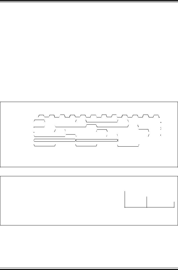
3.1Clocking Scheme/Instruction Cycle
The clock input (OSC1/CLKIN/RA7 pin) is internally divided by four to generate four non-overlapping quadrature clocks namely Q1, Q2, Q3 and Q4. Internally, the program counter (PC) is incremented every Q1, the instruction is fetched from the program memory and latched into the instruction register in Q4. The instruction is decoded and executed during the following Q1 through Q4. The clocks and instruction execution flow is shown in Figure 3-2.
FIGURE 3-2: CLOCK/INSTRUCTION CYCLE
3.2Instruction Flow/Pipelining
An “Instruction Cycle” consists of four Q cycles (Q1, Q2, Q3 and Q4). The instruction fetch and execute are pipelined such that fetch takes one instruction cycle while decode and execute takes another instruction cycle. However, due to the pipelining, each instruction effectively executes in one cycle. If an instruction causes the program counter to change (e.g., GOTO) then two cycles are required to complete the instruction (Example 3-1).
A fetch cycle begins with the program counter (PC) incrementing in Q1.
In the execution cycle, the fetched instruction is latched into the “Instruction Register (IR)” in cycle Q1. This instruction is then decoded and executed during the Q2, Q3, and Q4 cycles. Data memory is read during Q2 (operand read) and written during Q4 (destination write).
OSC1 |
|
|
Q1 |
|
Q2 |
|
Q3 |
Q4 |
|
Q1 |
Q2 |
|
Q3 |
|
Q4 |
|
|
Q1 |
|
|
Q2 |
|
|
Q3 |
|
Q4 |
|
|
|
|
|
|
|
|
|
|
|
|
|
|
|
|
|
||||||||||||||||||||
|
|
|
|
|
|
|
|
|
|
|
|
|
|
|
|
|
|
|
|
|
|
|
|
|
|
|
|
|
|
|
|
|
|
|
|
|
|
|
|
|
|
|
|
|
|
|
|
|
|
|
|
|
|
|
|
|
|
|
|
||||
Q1 |
|
|
|
|
|
|
|
|
|
|
|
|
|
|
|
|
|
|
|
|
|
|
|
|
|
|
|
|
|
|
|
|
|
|
|
|
|
|
|
|
|
|
|
|
|
|
|
|
|
|
|
|
|
|
|
|
|
|
|
||||
Q2 |
|
|
|
|
|
|
|
|
|
|
|
|
|
|
|
|
|
|
|
|
|
|
|
|
|
|
|
|
|
Internal |
|
|
|
|
|
|
|
|
|
|
|
|
|
|
|
|
|
|
|
|
|
|
|
|
|
|
|
|
|||||
|
|
|
|
|
|
|
|
|
|
|
|
|
|
|
|
|
|
|
|
|
|
|
|
|
|
|
|
|
|||
Q3 |
|
|
|
|
|
|
|
|
|
|
|
|
|
|
|
|
|
|
|
|
|
|
|
|
|
|
|
|
|
phase |
|
|
|
|
|
|
|
|
|
|
|
|
|
|
|
|
|
|
|
|
|
|
|
|
|
|
|
|
|
|
clock |
||
Q4 |
|
|
|
|
|
|
|
|
|
|
|
|
|
|
|
|
|
|
|
|
|
|
|
|
|
|
|
|
|
|
|
|
|
|
|
|
|
|
|
|
|
|
|
|
|
|
|
|
|
|
|
|
|
|
|
|
|
|
|
||||
|
|
|
|
|
|
|
|
|
|
|
|
|
|
|
|
|
|
|
|
|
|
|
|
|
|
|
|
|
|
||
PC |
|
|
|
|
|
PC |
|
|
|
PC+1 |
|
|
|
|
|
|
|
|
|
|
|
|
|
|
|
|
|||||
|
|
|
|
|
|
|
|
|
|
|
|
|
|
|
|
|
PC+2 |
|
|
|
|
|
|||||||||
OSC2/CLKOUT |
|
|
|
|
|
|
|
|
|
|
|
|
|
|
|
|
|
|
|
|
|
|
|
|
|
|
|
|
|
|
|
|
|
|
|
|
|
|
|
|
|
|
|
|
|
|
|
|
|
|
|
|
|
|
|
|
|
|
|
|
|
||
(ER mode) |
|
|
|
|
|
|
|
|
|
|
|
|
|
|
|
|
|
|
|
|
|
|
|
|
|
|
|
|
|
|
|
|
|
|
|
|
|
|
|
|
|
|
|
|
|
|
|
|
|
|
|
|
|
|
|
|
|
|
|
||||
|
|
|
|
|
|
Fetch INST (PC) |
|
|
|
|
|
|
|
|
|
|
|
|
|
|
|
|
|
|
|
|
|
|
|
||
|
|
|
|
|
Execute INST (PC-1) |
|
|
|
Fetch INST (PC+1) |
|
|
|
|
|
|
|
|
|
|
|
|
|
|
|
|
||||||
|
|
|
|
|
|
|
|
|
|
|
|
Execute INST (PC) |
|
|
|
|
|
Fetch INST (PC+2) |
|
|
|
|
|
||||||||
|
|
|
|
|
|
|
|
|
|
|
|
|
|
|
|
|
|
|
|
Execute INST (PC+1) |
|
|
|
|
|
||||||
|
|
|
|
|
|
|
|
|
|
|
|
|
|
|
|
|
|
|
|
|
|
|
|
|
|||||||
EXAMPLE 3-1: INSTRUCTION PIPELINE FLOW
1. |
MOVLW |
55h |
Fetch 1 |
Execute 1 |
|
|
|
|
|
|
|
|
|
|
|
|
|
2. |
MOVWF |
PORTB |
|
Fetch 2 |
Execute 2 |
|
|
|
|
|
|
|
|
|
|
|
|
3. |
CALL |
SUB_1 |
|
|
Fetch 3 |
Execute 3 |
|
|
|
|
|
|
|
|
|
|
|
4. |
BSF |
PORTA, BIT3 |
|
|
|
Fetch 4 |
Flush |
|
|
|
|
|
|
|
|
|
|
Fetch SUB_1 Execute SUB_1
All instructions are single cycle, except for any program branches. These take two cycles since the fetch instruction is “flushed” from the pipeline while the new instruction is being fetched and then executed.
DS40300B-page 12 |
Preliminary |
© 1999 Microchip Technology Inc. |
PIC16F62X
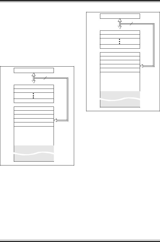
4.0MEMORY ORGANIZATION
4.1Program Memory Organization
The PIC16F62X has a 13-bit program counter capable of addressing an 8K x 14 program memory space. Only the first 1K x 14 (0000h - 03FFh) for the PIC16F627 and 2K x 14 (0000h - 07FFh) for the PIC16F628 are physically implemented. Accessing a location above these boundaries will cause a wrap-around within the first 1K x 14 space (PIC16F627) or 2K x 14 space (PIC16F628). The reset vector is at 0000h and the interrupt vector is at 0004h (Figure 4-1 and Figure 4-2).
FIGURE 4-1: PROGRAM MEMORY MAP AND STACK FOR THE PIC16F627
|
PC<12:0> |
|
CALL, RETURN |
13 |
|
RETFIE, RETLW |
|
|
Stack Level 1 |
|
|
Stack Level 2 |
|
|
Stack Level 8 |
|
|
Reset Vector |
000h |
|
|
|
|
Interrupt Vector |
0004 |
|
|
|
0005 |
On-chip Program |
|
|
|
Memory |
|
|
|
03FFh |
|
|
0400h |
|
|
1FFFh |
FIGURE 4-2: PROGRAM MEMORY MAP AND STACK FOR THE PIC16F628
|
PC<12:0> |
|
CALL, RETURN |
13 |
|
RETFIE, RETLW |
|
|
Stack Level 1 |
|
|
Stack Level 2 |
|
|
Stack Level 8 |
|
|
Reset Vector |
000h |
|
|
|
|
Interrupt Vector |
0004 |
|
|
|
0005 |
On-chip Program |
|
|
|
Memory |
|
|
|
07FFh |
|
|
0800h |
|
|
1FFFh |
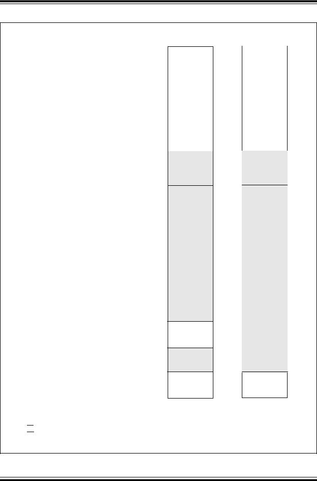
4.2Data Memory Organization
The data memory (Figure 4-3) is partitioned into four Banks which contain the general purpose registers and the special function registers. The Special Function Registers are located in the first 32 locations of each Bank. Register locations 20-7Fh, A0h-FFh, 120h-14Fh, 170h-17Fh and 1F0h-1FFh are general purpose registers implemented as static RAM.
The Table below lists how to access the four banks of registers:
|
RP1 |
RP0 |
|
|
|
|
|
|
Bank0 |
0 |
0 |
|
|
|
Bank1 |
0 |
1 |
|
|
|
Bank2 |
1 |
0 |
|
|
|
Bank3 |
1 |
1 |
|
|
|
Addresses F0h-FFh, 170h-17Fh and 1F0h-1FFh are implemented as common RAM and mapped back to addresses 70h-7Fh.
4.2.1GENERAL PURPOSE REGISTER FILE
The register file is organized as 224 x 8 in the PIC16F62X. Each is accessed either directly or indirectly through the File Select Register FSR (Section 4.4).
© 1999 Microchip Technology Inc.
Preliminary
DS40300B-page 13
PIC16F62X
FIGURE 4-3: DATA MEMORY MAP OF THE PIC16F627 AND PIC16F628
Indirect addr.(*) |
00h |
|
01h |
TMR0 |
|
|
02h |
PCL |
|
|
03h |
STATUS |
|
FSR |
04h |
|
05h |
PORTA |
|
|
06h |
PORTB |
|
|
07h |
|
08h |
|
09h |
PCLATH |
0Ah |
INTCON |
0Bh |
|
0Ch |
PIR1 |
|
|
0Dh |
TMR1L |
0Eh |
|
0Fh |
TMR1H |
|
|
10h |
T1CON |
|
|
11h |
TMR2 |
|
|
12h |
T2CON |
|
|
13h |
|
|
|
14h |
CCPR1L |
15h |
|
16h |
CCPR1H |
|
|
17h |
CCP1CON |
|
|
18h |
RCSTA |
|
TXREG |
19h |
RCREG |
1Ah |
|
1Bh |
|
1Ch |
|
1Dh |
|
1Eh |
CMCON |
1Fh |
|
20h |
|
|
General |
|
Purpose |
|
Register |
|
96 Bytes |
|
|
7Fh |
Bank 0 |
|
Indirect addr.(*) |
80h |
|
OPTION |
81h |
|
PCL |
82h |
|
STATUS |
83h |
|
FSR |
84h |
|
TRISA |
85h |
|
TRISB |
86h |
|
|
87h |
|
|
88h |
|
|
89h |
|
PCLATH |
8Ah |
|
INTCON |
8Bh |
|
PIE1 |
8Ch |
|
|
8Dh |
|
PCON |
8Eh |
|
|
8Fh |
|
|
90h |
|
|
91h |
|
PR2 |
92h |
|
|
93h |
|
|
94h |
|
|
95h |
|
|
96h |
|
|
97h |
|
TXSTA |
98h |
|
SPBRG |
99h |
|
EEDATA |
9Ah |
|
EEADR |
9Bh |
|
EECON1 |
9Ch |
|
EECON2* |
9Dh |
|
|
9Eh |
|
VRCON |
9Fh |
|
|
|
|
General |
A0h |
|
Purpose |
||
|
||
Register |
|
|
80 Bytes |
|
|
|
EFh |
|
accesses |
F0h |
|
|
||
70h-7Fh |
|
|
|
FFh |
|
Bank 1 |
||
|
Indirect addr.(*) |
100h |
TMR0 |
101h |
PCL |
102h |
|
103h |
STATUS |
|
|
104h |
FSR |
|
|
105h |
PORTB |
106h |
|
107h |
|
108h |
|
109h |
PCLATH |
10Ah |
INTCON |
10Bh |
|
10Ch |
|
|
|
10Dh |
|
10Eh |
|
|
|
10Fh |
|
11Fh
General 120h Purpose
Register
48 Bytes 14Fh
150h
16Fh
170h
accesses 70h-7Fh
17Fh
Bank 2
|
File |
|
Address |
|
|
Indirect addr.(*) |
180h |
OPTION |
181h |
PCL |
182h |
STATUS |
183h |
FSR |
184h |
|
185h |
TRISB |
186h |
|
187h |
|
188h |
|
189h |
PCLATH |
18Ah |
INTCON |
18Bh |
|
18Ch |
|
18Dh |
|
18Eh |
|
18Fh |
1EFh
1F0h
accesses 70h - 7Fh
1FFh
Bank 3

 Unimplemented data memory locations, read as ’0’. * Not a physical register.
DS40300B-page 14 |
Preliminary |
© 1999 Microchip Technology Inc. |

PIC16F62X
4.2.2SPECIAL FUNCTION REGISTERS
The special function registers are registers used by the CPU and Peripheral functions for controlling the desired operation of the device (Table 4-1). These registers are static RAM.
The special registers can be classified into two sets (core and peripheral). The special function registers associated with the “core” functions are described in this section. Those related to the operation of the peripheral features are described in the section of that peripheral feature.
TABLE 4-1: |
SPECIAL REGISTERS SUMMARY BANK0 |
|
|
|
|
|
|
|
|||||||||
|
|
|
|
|
|
|
|
|
|
|
|
|
|
|
|
||
|
|
|
|
|
|
|
|
|
|
|
|
|
|
Value on |
Value on |
||
Address |
Name |
Bit 7 |
Bit 6 |
Bit 5 |
|
Bit 4 |
Bit 3 |
Bit 2 |
Bit 1 |
Bit 0 |
POR |
all other |
|||||
|
|
|
|
|
|
|
|
|
|
|
|
|
|
Reset |
Resets(1) |
||
|
|
|
|
|
|
|
|
|
|
|
|
|
|
|
|
|
|
Bank 0 |
|
|
|
|
|
|
|
|
|
|
|
|
|
|
|
|
|
00h |
INDF |
|
Addressing this location uses contents of FSR to address data memory (not a physical register) |
xxxx xxxx |
xxxx xxxx |
||||||||||||
01h |
TMR0 |
|
Timer0 Module’s Register |
|
|
|
|
|
|
|
|
xxxx xxxx |
uuuu uuuu |
||||
02h |
PCL |
|
Program Counter's (PC) Least Significant Byte |
|
|
|
|
|
0000 |
0000 |
0000 |
0000 |
|||||
03h |
STATUS |
|
IRP |
RP1 |
RP0 |
|
TO |
|
PD |
|
Z |
DC |
C |
0001 |
1xxx |
000q |
quuu |
04h |
FSR |
|
Indirect data memory address pointer |
|
|
|
|
|
xxxx xxxx |
uuuu uuuu |
|||||||
05h |
PORTA |
|
RA7 |
RA6 |
RA5 |
|
RA4 |
RA3 |
RA2 |
RA1 |
RA0 |
xxxx 0000 |
xxxx 0000 |
||||
06h |
PORTB |
|
RB7 |
RB6 |
RB5 |
RB4 |
RB3 |
RB2 |
RB1 |
RB0 |
xxxx xxxx |
uuuu uuuu |
|||||
07h |
Unimplemented |
|
|
|
|
|
|
|
|
|
|
|
|
— |
— |
||
08h |
Unimplemented |
|
|
|
|
|
|
|
|
|
|
|
|
— |
— |
||
09h |
Unimplemented |
|
|
|
|
|
|
|
|
|
|
|
|
— |
— |
||
0Ah |
PCLATH |
|
— |
— |
— |
Write buffer for upper 5 bits of program counter |
|
---0 0000 |
---0 0000 |
||||||||
0Bh |
INTCON |
|
GIE |
PEIE |
T0IE |
INTE |
RBIE |
T0IF |
INTF |
RBIF |
0000 |
000x |
0000 |
000u |
|||
0Ch |
PIR1 |
|
EEIF |
CMIF |
RCIF |
|
TXIF |
|
— |
CCP1IF |
TMR2IF |
TMR1IF |
0000 |
-000 |
0000 |
-000 |
|
0Dh |
Unimplemented |
|
|
|
|
|
|
|
|
|
|
|
|
— |
— |
||
0Eh |
TMR1L |
|
Holding register for the least significant byte of the 16-bit TMR1 |
|
|
xxxx xxxx |
uuuu uuuu |
||||||||||
0Fh |
TMR1H |
|
Holding register for the most significant byte of the 16-bit TMR1 |
|
|
xxxx xxxx |
uuuu uuuu |
||||||||||
10h |
T1CON |
|
— |
— |
T1CKPS1 |
T1CKPS0 |
T1OSCEN |
T1SYNC |
TMR1CS |
TMR1ON |
--00 0000 |
--uu uuuu |
|||||
11h |
TMR2 |
|
TMR2 module’s register |
|
|
|
|
|
|
|
|
0000 |
0000 |
0000 |
0000 |
||
12h |
T2CON |
|
— |
TOUTPS3 |
TOUTPS2 |
TOUTPS1 |
TOUTPS0 |
TMR2ON |
T2CKPS1 |
T2CKPS0 |
-000 0000 |
-uuu uuuu |
|||||
13h |
Unimplemented |
|
|
|
|
|
|
|
|
|
|
|
|
— |
— |
||
14h |
Unimplemented |
|
|
|
|
|
|
|
|
|
|
|
|
— |
— |
||
15h |
CCPR1L |
|
Capture/Compare/PWM register (LSB) |
|
|
|
|
|
xxxx xxxx |
uuuu uuuu |
|||||||
16h |
CCPR1H |
Capture/Compare/PWM register (MSB) |
|
|
|
|
|
xxxx xxxx |
uuuu uuuu |
||||||||
17h |
CCP1CON |
— |
— |
CCP1X |
CCP1Y |
CCP1M3 |
CCP1M2 |
CCP1M1 |
CCP1M0 |
--00 0000 |
--00 0000 |
||||||
18h |
RCSTA |
|
SPEN |
RX9 |
SREN |
|
CREN |
ADEN |
FERR |
OERR |
RX9D |
0000 |
-00x |
0000 |
-00x |
||
19h |
TXREG |
|
USART Transmit data register |
|
|
|
|
|
|
|
|
0000 |
0000 |
0000 |
0000 |
||
1Ah |
RCREG |
|
USART Receive data register |
|
|
|
|
|
|
|
|
0000 |
0000 |
0000 |
0000 |
||
1Bh |
Unimplemented |
|
|
|
|
|
|
|
|
|
|
|
|
— |
— |
||
1Ch |
Unimplemented |
|
|
|
|
|
|
|
|
|
|
|
|
— |
— |
||
1Dh |
Unimplemented |
|
|
|
|
|
|
|
|
|
|
|
|
— |
— |
||
1Eh |
Unimplemented |
|
|
|
|
|
|
|
|
|
|
|
|
— |
— |
||
1Fh |
CMCON |
|
C2OUT |
C1OUT |
C2INV |
|
C1INV |
CIS |
CM2 |
CM1 |
CM0 |
0000 |
0000 |
0000 |
0000 |
||
Legend: — = Unimplemented locations read as ‘0’, u = unchanged, x = unknown, q = value depends on condition, shaded = unimplemented
Note 1: Other (non power-up) resets include MCLR Reset, Brown-out Detect and Watchdog Timer Reset during normal operation.
© 1999 Microchip Technology Inc.
Preliminary
DS40300B-page 15

PIC16F62X
TABLE 4-2: |
SPECIAL FUNCTION REGISTERS SUMMARY BANK1 |
|
|
|
|
|
|
|
|||||||||||||
|
|
|
|
|
|
|
|
|
|
|
|
|
|
|
|
|
|
|
|
||
|
|
|
|
|
|
|
|
|
|
|
|
|
|
|
|
|
|
Value on |
Value on |
||
Address |
Name |
Bit 7 |
Bit 6 |
Bit 5 |
Bit 4 |
Bit 3 |
Bit 2 |
|
Bit 1 |
|
Bit 0 |
POR |
all other |
||||||||
|
|
|
|
|
|
|
|
|
|
|
|
|
|
|
|
|
|
Reset |
resets(1) |
||
|
|
|
|
|
|
|
|
|
|
|
|
|
|
|
|
|
|
|
|
|
|
Bank 1 |
|
|
|
|
|
|
|
|
|
|
|
|
|
|
|
|
|
|
|
|
|
80h |
INDF |
|
Addressing this location uses contents of FSR to address data memory (not a physical reg- |
xxxx xxxx |
xxxx xxxx |
||||||||||||||||
|
|
|
ister) |
|
|
|
|
|
|
|
|
|
|
|
|
|
|
|
|
|
|
81h |
OPTION |
|
RBPU |
|
INTEDG |
T0CS |
T0SE |
PSA |
PS2 |
PS1 |
PS0 |
1111 |
1111 |
1111 |
1111 |
||||||
82h |
PCL |
|
Program Counter’s (PC) Least Significant Byte |
|
|
|
|
|
|
|
0000 |
0000 |
0000 |
0000 |
|||||||
83h |
STATUS |
|
IRP |
RP1 |
RP0 |
TO |
|
PD |
|
Z |
|
DC |
|
C |
0001 |
1xxx |
000q |
quuu |
|||
84h |
FSR |
|
Indirect data memory address pointer |
|
|
|
|
|
|
|
|
|
xxxx xxxx |
uuuu uuuu |
|||||||
85h |
TRISA |
|
TRISA7 |
TRISA6 |
— |
TRISA4 |
TRISA3 |
TRISA2 |
TRISA1 |
TRISA0 |
11-1 1111 |
11-1 1111 |
|||||||||
86h |
TRISB |
|
TRISB7 |
TRISB6 |
TRISB5 |
TRISB4 |
TRISB3 |
TRISB2 |
TRISB1 |
TRISB0 |
1111 |
1111 |
1111 |
1111 |
|||||||
87h |
Unimplemented |
|
|
|
|
|
|
|
|
|
|
|
|
|
|
|
|
— |
|
— |
|
88h |
Unimplemented |
|
|
|
|
|
|
|
|
|
|
|
|
|
|
|
|
— |
|
— |
|
89h |
Unimplemented |
|
|
|
|
|
|
|
|
|
|
|
|
|
|
|
|
— |
|
— |
|
8Ah |
PCLATH |
— |
— |
— |
Write buffer for upper 5 bits of program counter |
---0 0000 |
---0 0000 |
||||||||||||||
8Bh |
INTCON |
|
GIE |
PEIE |
T0IE |
INTE |
RBIE |
T0IF |
INTF |
RBIF |
0000 |
000x |
0000 |
000u |
|||||||
8Ch |
PIE1 |
|
EEIE |
CMIE |
RCIE |
TXIE |
|
— |
CCP1IE |
TMR2IE |
TMR1IE |
0000 |
-000 |
0000 |
-000 |
||||||
8Dh |
Unimplemented |
|
|
|
|
|
|
|
|
|
|
|
|
|
|
|
|
— |
|
— |
|
8Eh |
PCON |
|
— |
— |
— |
|
— |
OSCF |
— |
|
POR |
|
|
BOD |
|
---- 1-0x |
---- 1-uq |
||||
8Fh |
Unimplemented |
|
|
|
|
|
|
|
|
|
|
|
|
|
|
|
|
|
|
|
|
90h |
Unimplemented |
|
|
|
|
|
|
|
|
|
|
|
|
|
|
|
|
— |
|
— |
|
91h |
Unimplemented |
|
|
|
|
|
|
|
|
|
|
|
|
|
|
|
|
— |
|
— |
|
92h |
PR2 |
|
Timer2 Period Register |
|
|
|
|
|
|
|
|
|
|
|
|
11111111 |
11111111 |
||||
93h |
Unimplemented |
|
|
|
|
|
|
|
|
|
|
|
|
|
|
|
|
— |
|
— |
|
94h |
Unimplemented |
|
|
|
|
|
|
|
|
|
|
|
|
|
|
|
|
— |
|
— |
|
95h |
Unimplemented |
|
|
|
|
|
|
|
|
|
|
|
|
|
|
|
|
— |
|
— |
|
96h |
Unimplemented |
|
|
|
|
|
|
|
|
|
|
|
|
|
|
|
|
— |
|
— |
|
97h |
Unimplemented |
|
|
|
|
|
|
|
|
|
|
|
|
|
|
|
|
— |
|
— |
|
98h |
TXSTA |
|
CSRC |
TX9 |
TXEN |
SYNC |
|
— |
BRGH |
TRMT |
TX9D |
0000 |
-010 |
0000 |
-010 |
||||||
99h |
SPBRG |
|
Baud Rate Generator Register |
|
|
|
|
|
|
|
|
|
|
|
0000 |
0000 |
0000 |
0000 |
|||
9Ah |
EEDATA |
EEPROM data register |
|
|
|
|
|
|
|
|
|
|
|
|
xxxx xxxx |
uuuu uuuu |
|||||
9Bh |
EEADR |
|
— |
EEPROM address register |
|
|
|
|
|
|
|
|
|
xxxx xxxx |
uuuu uuuu |
||||||
9Ch |
EECON1 |
— |
— |
— |
|
— |
WRERR |
WREN |
WR |
RD |
---- x000 |
---- q000 |
|||||||||
9Dh |
EECON2 |
EEPROM control register 2 (not a physical register) |
|
|
|
|
|
|
|
-------- |
-------- |
||||||||||
9Eh |
Unimplemented |
|
|
|
|
|
|
|
|
|
|
|
|
|
|
|
|
— |
|
— |
|
9Fh |
VRCON |
|
VREN |
VROE |
VRR |
|
— |
VR3 |
VR2 |
VR1 |
VR0 |
0000000 |
0000000 |
||||||||
Legend: : — = Unimplemented locations read as ‘0’, u = unchanged, x = unknown, q = value depends on condition, shaded = unimplemented
Note 1: Other (non power-up) resets include MCLR Reset, Brown-out Detect and Watchdog Timer Reset during normal operation.
DS40300B-page 16 |
Preliminary |
© 1999 Microchip Technology Inc. |

PIC16F62X
TABLE 4-3: |
SPECIAL FUNCTION REGISTERS SUMMARY BANK2 |
|
|
|
|||||||||||||
|
|
|
|
|
|
|
|
|
|
|
|
|
|
|
|
|
|
|
|
|
|
|
|
|
|
|
|
|
|
|
|
|
|
Value on |
Value on |
Address |
Name |
Bit 7 |
Bit 6 |
Bit 5 |
|
Bit 4 |
|
Bit 3 |
Bit 2 |
Bit 1 |
Bit 0 |
POR |
all other |
||||
|
|
|
|
|
|
|
|
|
|
|
|
|
|
|
|
Reset |
resets(1) |
|
|
|
|
|
|
|
|
|
|
|
|
|
|
|
|
|
|
Bank 1 |
|
|
|
|
|
|
|
|
|
|
|
|
|
|
|
|
|
100h |
INDF |
|
Addressing this location uses contents of FSR to address data memory (not a physical reg- |
xxxx xxxx |
xxxx xxxx |
||||||||||||
|
|
|
ister) |
|
|
|
|
|
|
|
|
|
|
|
|
|
|
101h |
TMR0 |
|
RBPU |
|
INTEDG |
T0CS |
T0SE |
|
PSA |
PS2 |
PS1 |
PS0 |
1111 1111 |
1111 1111 |
|||
102h |
PCL |
|
Program Counter’s (PC) Least Significant Byte |
|
|
|
|
|
0000 0000 |
0000 0000 |
|||||||
103h |
STATUS |
|
IRP |
RP1 |
RP0 |
|
TO |
|
|
PD |
|
Z |
DC |
C |
0001 1xxx |
000q quuu |
|
104h |
FSR |
|
Indirect data memory address pointer |
|
|
|
|
|
xxxx xxxx |
uuuu uuuu |
|||||||
105h |
Unimplemented |
|
|
|
|
|
|
|
|
|
|
|
|
|
— |
— |
|
106h |
PORTB |
|
TRISB7 |
TRISB6 |
TRISB5 |
TRISB4 |
|
TRISB3 |
TRISB2 |
TRISB1 |
TRISB0 |
1111 1111 |
1111 1111 |
||||
107h |
Unimplemented |
|
|
|
|
|
|
|
|
|
|
|
|
|
— |
— |
|
108h |
Unimplemented |
|
|
|
|
|
|
|
|
|
|
|
|
|
— |
— |
|
109h |
Unimplemented |
|
|
|
|
|
|
|
|
|
|
|
|
|
— |
— |
|
10Ah |
PCLATH |
— |
— |
— |
Write buffer for upper 5 bits of program counter |
---0 0000 |
---0 0000 |
||||||||||
10Bh |
INTCON |
GIE |
PEIE |
T0IE |
|
INTE |
|
RBIE |
T0IF |
INTF |
RBIF |
0000 000x |
0000 000u |
||||
10Ch |
|
|
|
|
|
|
|
|
|
|
|
|
|
|
|
— |
— |
10Dh |
Unimplemented |
|
|
|
|
|
|
|
|
|
|
|
|
|
— |
— |
|
10Eh |
|
|
|
|
|
|
|
|
|
|
|
|
|
|
|
— |
— |
10Fh |
Unimplemented |
|
|
|
|
|
|
|
|
|
|
|
|
|
|
|
|
110h |
Unimplemented |
|
|
|
|
|
|
|
|
|
|
|
|
|
— |
— |
|
111h |
Unimplemented |
|
|
|
|
|
|
|
|
|
|
|
|
|
— |
— |
|
112h |
|
|
|
|
|
|
|
|
|
|
|
|
|
|
|
|
|
113h |
Unimplemented |
|
|
|
|
|
|
|
|
|
|
|
|
|
— |
— |
|
114h |
Unimplemented |
|
|
|
|
|
|
|
|
|
|
|
|
|
— |
— |
|
115h |
Unimplemented |
|
|
|
|
|
|
|
|
|
|
|
|
|
— |
— |
|
116h |
Unimplemented |
|
|
|
|
|
|
|
|
|
|
|
|
|
— |
— |
|
117h |
Unimplemented |
|
|
|
|
|
|
|
|
|
|
|
|
|
— |
— |
|
118h |
|
|
|
|
|
|
|
|
|
|
|
|
|
|
|
— |
— |
119h |
|
|
|
|
|
|
|
|
|
|
|
|
|
|
|
— |
— |
11Ah |
|
|
|
|
|
|
|
|
|
|
|
|
|
|
|
— |
— |
11Bh |
|
|
|
|
|
|
|
|
|
|
|
|
|
|
|
— |
— |
11Ch |
|
|
|
|
|
|
|
|
|
|
|
|
|
|
|
— |
— |
11Dh |
|
|
|
|
|
|
|
|
|
|
|
|
|
|
|
— |
— |
11Eh |
Unimplemented |
|
|
|
|
|
|
|
|
|
|
|
|
|
— |
— |
|
11Fh |
|
|
|
|
|
|
|
|
|
|
|
|
|
|
|
— |
— |
Legend: — = Unimplemented locations read as ‘0’, u = unchanged, x = unknown, q = value depends on condition, shaded = unimplemented
Note 1: Other (non power-up) resets include MCLR Reset, Brown-out Detect and Watchdog Timer Reset during normal operation.
© 1999 Microchip Technology Inc.
Preliminary
DS40300B-page 17

PIC16F62X
TABLE 4-4: |
SPECIAL FUNCTION REGISTERS SUMMARY BANK3 |
|
|
|
|||||||||||||
|
|
|
|
|
|
|
|
|
|
|
|
|
|
|
|
|
|
|
|
|
|
|
|
|
|
|
|
|
|
|
|
|
|
Value on |
Value on |
Address |
Name |
Bit 7 |
Bit 6 |
Bit 5 |
|
Bit 4 |
|
Bit 3 |
Bit 2 |
Bit 1 |
Bit 0 |
POR |
all other |
||||
|
|
|
|
|
|
|
|
|
|
|
|
|
|
|
|
Reset |
resets(1) |
|
|
|
|
|
|
|
|
|
|
|
|
|
|
|
|
|
|
Bank 1 |
|
|
|
|
|
|
|
|
|
|
|
|
|
|
|
|
|
180h |
INDF |
|
Addressing this location uses contents of FSR to address data memory (not a physical reg- |
xxxx xxxx |
xxxx xxxx |
||||||||||||
|
|
|
ister) |
|
|
|
|
|
|
|
|
|
|
|
|
|
|
181h |
OPTION |
RBPU |
|
INTEDG |
T0CS |
T0SE |
|
PSA |
PS2 |
PS1 |
PS0 |
1111 1111 |
1111 1111 |
||||
182h |
PCL |
|
Program Counter’s (PC) Least Significant Byte |
|
|
|
|
|
0000 0000 |
0000 0000 |
|||||||
183h |
STATUS |
|
IRP |
RP1 |
RP0 |
|
TO |
|
|
PD |
|
Z |
DC |
C |
0001 1xxx |
000q quuu |
|
184h |
FSR |
|
Indirect data memory address pointer |
|
|
|
|
|
xxxx xxxx |
uuuu uuuu |
|||||||
185h |
Unimplemented |
|
|
|
|
|
|
|
|
|
|
|
|
|
— |
— |
|
186h |
TRISB |
|
TRISB7 |
TRISB6 |
TRISB5 |
TRISB4 |
|
TRISB3 |
TRISB2 |
TRISB1 |
TRISB0 |
1111 1111 |
1111 1111 |
||||
187h |
Unimplemented |
|
|
|
|
|
|
|
|
|
|
|
|
|
— |
— |
|
188h |
Unimplemented |
|
|
|
|
|
|
|
|
|
|
|
|
|
— |
— |
|
189h |
Unimplemented |
|
|
|
|
|
|
|
|
|
|
|
|
|
— |
— |
|
18Ah |
PCLATH |
— |
— |
— |
Write buffer for upper 5 bits of program counter |
---0 0000 |
---0 0000 |
||||||||||
18Bh |
INTCON |
GIE |
PEIE |
T0IE |
|
INTE |
|
RBIE |
T0IF |
INTF |
RBIF |
0000 000x |
0000 000u |
||||
18Ch |
|
|
|
|
|
|
|
|
|
|
|
|
|
|
|
|
|
18Dh |
|
|
|
|
|
|
|
|
|
|
|
|
|
|
|
|
|
18Eh |
|
|
|
|
|
|
|
|
|
|
|
|
|
|
|
|
|
18Fh |
|
|
|
|
|
|
|
|
|
|
|
|
|
|
|
|
|
190h |
|
|
|
|
|
|
|
|
|
|
|
|
|
|
|
|
|
191h |
|
|
|
|
|
|
|
|
|
|
|
|
|
|
|
|
|
192h |
|
|
|
|
|
|
|
|
|
|
|
|
|
|
|
|
|
193h |
|
|
|
|
|
|
|
|
|
|
|
|
|
|
|
|
|
194h |
|
|
|
|
|
|
|
|
|
|
|
|
|
|
|
|
|
195h |
|
|
|
|
|
|
|
|
|
|
|
|
|
|
|
|
|
196h |
|
|
|
|
|
|
|
|
|
|
|
|
|
|
|
|
|
197h |
|
|
|
|
|
|
|
|
|
|
|
|
|
|
|
|
|
198h |
|
|
|
|
|
|
|
|
|
|
|
|
|
|
|
|
|
199h |
|
|
|
|
|
|
|
|
|
|
|
|
|
|
|
|
|
19Ah |
|
|
|
|
|
|
|
|
|
|
|
|
|
|
|
|
|
19Bh |
|
|
|
|
|
|
|
|
|
|
|
|
|
|
|
|
|
19Ch |
|
|
|
|
|
|
|
|
|
|
|
|
|
|
|
|
|
19Dh |
|
|
|
|
|
|
|
|
|
|
|
|
|
|
|
|
|
19Eh |
|
|
|
|
|
|
|
|
|
|
|
|
|
|
|
|
|
19Fh |
|
|
|
|
|
|
|
|
|
|
|
|
|
|
|
|
|
Legend: — = Unimplemented locations read as ‘0’, u = unchanged, x = unknown, q = value depends on condition, shaded = unimplemented
Note 1: Other (non power-up) resets include MCLR Reset, Brown-out Detect and Watchdog Timer Reset during normal operation.
DS40300B-page 18 |
Preliminary |
© 1999 Microchip Technology Inc. |

PIC16F62X
4.2.2.1STATUS REGISTER
The STATUS register, shown in Register 4-1, contains the arithmetic status of the ALU, the RESET status and the bank select bits for data memory (SRAM).
The STATUS register can be the destination for any instruction, like any other register. If the STATUS register is the destination for an instruction that affects the Z, DC or C bits, then the write to these three bits is disabled. These bits are set or cleared according to the device logic. Furthermore, the TO and PD bits are not writable. Therefore, the result of an instruction with the STATUS register as destination may be different than intended.
For example, CLRF STATUS will clear the upper-three bits and set the Z bit. This leaves the status register as 000uu1uu (where u = unchanged).
It is recommended, therefore, that only BCF, BSF, SWAPF and MOVWF instructions are used to alter the STATUS register because these instructions do not affect any status bit. For other instructions, not affecting any status bits, see the “Instruction Set Summary”.
Note 1: The C and DC bits operate as a Borrow and Digit Borrow out bit, respectively, in subtraction. See the SUBLW and SUBWF instructions for examples.
REGISTER 4-1: STATUS REGISTER (ADDRESS 03H OR 83H)
R/W-0 |
R/W-0 |
R/W-0 R-1 |
R-1 |
R/W-x |
R/W-x R/W-x |
||||||
IRP |
RP1 |
RP0 |
|
TO |
|
|
PD |
|
Z |
DC |
C |
bit7 |
|
|
|
|
|
|
|
|
|
|
bit0 |
bit 7: IRP: Register Bank Select bit (used for indirect addressing) 1 = Bank 2, 3 (100h - 1FFh)
0 = Bank 0, 1 (00h - FFh)
bit 6-5: RP1:RP0: Register Bank Select bits (used for direct addressing) |
||
11 |
= Bank 3 |
(180h - 1FFh) |
10 |
= Bank 2 |
(100h - 17Fh) |
01 |
= Bank 1 |
(80h - FFh) |
00 |
= Bank 0 |
(00h - 7Fh) |
bit |
4: |
TO: Time-out bit |
||
|
|
1 |
= After power-up, CLRWDT instruction, or SLEEP instruction |
|
|
|
0 |
= A WDT time-out occurred |
|
bit |
3: |
|
: Power-down bit |
|
PD |
||||
|
|
1 |
= After power-up or by the CLRWDT instruction |
|
|
|
0 |
= By execution of the SLEEP instruction |
|
R = Readable bit W = Writable bit
U = Unimplemented bit, read as ’0’
-n = Value at POR reset
-x = Unknown at POR reset
bit |
2: |
Z: Zero bit |
|||||||
|
|
1 |
= The result of an arithmetic or logic operation is zero |
||||||
|
|
0 |
= The result of an arithmetic or logic operation is not zero |
||||||
bit |
1: |
|
|
|
|
|
|
|
|
DC: Digit carry/borrow |
bit (ADDWF, ADDLW,SUBLW,SUBWF instructions)(for borrow the polarity is reversed) |
||||||||
|
|
1 |
= A carry-out from the 4th low order bit of the result occurred |
||||||
|
|
0 |
= No carry-out from the 4th low order bit of the result |
||||||
bit |
0: |
|
|
bit (ADDWF, ADDLW,SUBLW,SUBWF instructions) |
|||||
C: Carry/borrow |
|||||||||
|
|
1 |
= A carry-out from the most significant bit of the result occurred |
||||||
|
|
0 |
= No carry-out from the most significant bit of the result occurred |
||||||
Note: For borrow the polarity is reversed. A subtraction is executed by adding the two’s complement of the second operand. For rotate (RRF, RLF) instructions, this bit is loaded with either the high or low order bit of the source register.
© 1999 Microchip Technology Inc.
Preliminary
DS40300B-page 19

PIC16F62X
4.2.2.2OPTION REGISTER
The OPTION register is a readable and writable register which contains various control bits to configure the TMR0/WDT prescaler, the external RB0/INT interrupt, TMR0, and the weak pull-ups on PORTB.
Note: To achieve a 1:1 prescaler assignment for TMR0, assign the prescaler to the WDT (PSA = 1). See Section 6.3.1
REGISTER 4-2: OPTION REGISTER (ADDRESS 81H)
|
|
R/W-1 R/W-1 |
R/W-1 |
R/W-1 |
|
R/W-1 R/W-1 |
R/W-1 |
R/W-1 |
|
|
|
|||||||||||
|
|
RBPU |
|
INTEDG |
T0CS |
|
T0SE |
|
PSA |
PS2 |
PS1 |
PS0 |
|
R = Readable bit |
|
|||||||
|
|
bit7 |
|
|
|
|
|
|
|
|
|
|
|
|
|
|
bit0 |
|
W = Writable bit |
|
||
|
|
|
|
|
|
|
|
|
|
|
|
|
|
|
|
|
|
|
|
|
-n = Value at POR reset |
|
|
|
bit 7: |
|
|
|
: PORTB Pull-up Enable bit |
|
|
|
|
|
|
||||||||||
|
|
RBPU |
|
|
|
|
|
|
||||||||||||||
|
|
|
|
|
1 |
= PORTB pull-ups are disabled |
|
|
|
|
|
|
||||||||||
|
|
|
|
|
0 |
= PORTB pull-ups are enabled by individual port latch values |
|
|
|
|||||||||||||
|
|
bit |
6: |
|
INTEDG: Interrupt Edge Select bit |
|
|
|
|
|
|
|||||||||||
|
|
|
|
|
1 |
= Interrupt on rising edge of RB0/INT pin |
|
|
|
|
|
|||||||||||
|
|
|
|
|
0 |
= Interrupt on falling edge of RB0/INT pin |
|
|
|
|
|
|||||||||||
|
|
bit |
5: |
|
T0CS: TMR0 Clock Source Select bit |
|
|
|
|
|
|
|||||||||||
|
|
|
|
|
1 |
= Transition on RA4/T0CKI pin |
|
|
|
|
|
|
||||||||||
|
|
|
|
|
0 |
= Internal instruction cycle clock (CLKOUT) |
|
|
|
|
|
|||||||||||
|
|
bit |
4: |
|
T0SE: TMR0 Source Edge Select bit |
|
|
|
|
|
|
|||||||||||
|
|
|
|
|
1 |
= Increment on high-to-low transition on RA4/T0CKI pin |
|
|
|
|
||||||||||||
|
|
|
|
|
0 |
= Increment on low-to-high transition on RA4/T0CKI pin |
|
|
|
|
||||||||||||
|
|
bit |
3: |
|
PSA: Prescaler Assignment bit |
|
|
|
|
|
|
|||||||||||
|
|
|
|
|
1 |
= Prescaler is assigned to the WDT |
|
|
|
|
|
|
||||||||||
|
|
|
|
|
0 |
= Prescaler is assigned to the Timer0 module |
|
|
|
|
|
|||||||||||
|
|
bit |
2-0: |
PS2:PS0: Prescaler Rate Select bits |
|
|
|
|
|
|
||||||||||||
|
|
|
|
|
|
Bit Value |
TMR0 Rate WDT Rate |
|
|
|
|
|
|
|||||||||
|
|
|
|
|
|
|
|
|
|
|
|
|
|
|
|
|
|
|
|
|
||
|
|
|
|
|
|
|
000 |
1 |
: 2 |
|
|
1 |
: 1 |
|
|
|
|
|
|
|
||
|
|
|
|
|
|
|
001 |
1 |
: 4 |
|
|
1 |
: 2 |
|
|
|
|
|
|
|
||
|
|
|
|
|
|
|
010 |
1 |
: 8 |
|
|
1 |
: 4 |
|
|
|
|
|
|
|
||
|
|
|
|
|
|
|
011 |
1 |
: 16 |
|
|
1 |
: 8 |
|
|
|
|
|
|
|
||
|
|
|
|
|
|
|
100 |
1 |
: 32 |
|
|
1 |
: 16 |
|
|
|
|
|
|
|
||
|
|
|
|
|
|
|
101 |
1 |
: 64 |
|
|
1 |
: 32 |
|
|
|
|
|
|
|
||
|
|
|
|
|
|
|
110 |
1 |
: 128 |
|
1 |
: 64 |
|
|
|
|
|
|
|
|||
|
|
|
|
|
|
|
111 |
1 |
: 256 |
|
1 |
: 128 |
|
|
|
|
|
|
|
|||
|
|
|
|
|
|
|
|
|
|
|
|
|
|
|
|
|
|
|
|
|
|
|
DS40300B-page 20 |
Preliminary |
© 1999 Microchip Technology Inc. |
PIC16F62X
4.2.2.3 |
INTCON REGISTER |
|
|
|||
The INTCON register |
is |
a readable and |
writable |
Note: Interrupt flag bits get set when an interrupt |
||
condition occurs regardless of the state of |
||||||
register which contains the various enable and flag bits |
||||||
its corresponding enable bit or the global |
||||||
for all interrupt sources except the comparator module. |
||||||
enable bit, GIE (INTCON<7>). |
||||||
See Section 4.2.2.4 |
and |
Section 4.2.2.5 |
for a |
|||
|
||||||
description of the comparator enable and flag bits.
REGISTER 4-3: INTCON REGISTER (ADDRESS 0BH OR 8BH)
R/W-0 |
R/W-0 |
R/W-0 |
R/W-0 |
R/W-0 R/W-0 |
R/W-0 R/W-x |
||
GIE |
PEIE |
T0IE |
INTE |
RBIE |
T0IF |
INTF |
RBIF |
bit7 |
|
|
|
|
|
|
bit0 |
R = Readable bit W = Writable bit
U = Unimplemented bit, read as ’0’
-n = Value at POR reset
-x = Unknown at POR reset
bit 7: |
GIE: Global Interrupt Enable bit |
||
|
|
1 |
= Enables all un-masked interrupts |
|
|
0 |
= Disables all interrupts |
bit |
6: |
PEIE: Peripheral Interrupt Enable bit |
|
|
|
1 |
= Enables all un-masked peripheral interrupts |
|
|
0 |
= Disables all peripheral interrupts |
bit |
5: |
T0IE: TMR0 Overflow Interrupt Enable bit |
|
|
|
1 |
= Enables the TMR0 interrupt |
|
|
0 |
= Disables the TMR0 interrupt |
bit |
4: |
INTE: RB0/INT External Interrupt Enable bit |
|
|
|
1 |
= Enables the RB0/INT external interrupt |
|
|
0 |
= Disables the RB0/INT external interrupt |
bit |
3: |
RBIE: RB Port Change Interrupt Enable bit |
|
|
|
1 |
= Enables the RB port change interrupt |
|
|
0 |
= Disables the RB port change interrupt |
bit |
2: |
T0IF: TMR0 Overflow Interrupt Flag bit |
|
|
|
1 |
= TMR0 register has overflowed (must be cleared in software) |
|
|
0 |
= TMR0 register did not overflow |
bit |
1: |
INTF: RB0/INT External Interrupt Flag bit |
|
|
|
1 |
= The RB0/INT external interrupt occurred (must be cleared in software) |
|
|
0 |
= The RB0/INT external interrupt did not occur |
bit |
0: |
RBIF: RB Port Change Interrupt Flag bit |
|
|
|
1 |
= When at least one of the RB7:RB4 pins changed state (must be cleared in software) |
|
|
0 |
= None of the RB7:RB4 pins have changed state |
|
|
|
|
© 1999 Microchip Technology Inc.
Preliminary
DS40300B-page 21

PIC16F62X
4.2.2.4PIE1 REGISTER
This register contains interrupt enable bits.
REGISTER 4-4: PIE1 REGISTER (ADDRESS 8CH)
R/W-0 R/W-0 R/W-0 |
R/W-0 |
U |
R/W-0 |
R/W-0 R/W-0 |
|||||
EEIE |
CMIE |
RCIE |
TXIE |
- |
CCP1IE |
TMR2IE |
TMR1IE |
||
bit7 |
|
|
|
|
|
|
|
bit0 |
|
bit 7: |
EEIE: EE Write Complete Interrupt Enable Bit |
|
|
||||||
|
|
1 |
= Enables the EE write complete interrupt |
|
|
||||
|
|
0 |
= Disables the EE write complete interrupt |
|
|
||||
bit |
6: |
CMIE: Comparator Interrupt Enable bit |
|
|
|
||||
|
|
1 |
= Enables the comparator interrupt |
|
|
|
|||
|
|
0 |
= Disables the comparator interrupt |
|
|
|
|||
bit |
5: |
RCIE: USART Receive Interrupt Enable bit |
|
|
|||||
|
|
1 |
= Enables the USART receive interrupt |
|
|
||||
|
|
0 |
= Disables the USART receive interrupt |
|
|
||||
bit |
4: |
TXIE: USART Transmit Interrupt Enable bit |
|
|
|||||
|
|
1 |
= Enables the USART transmit interrupt |
|
|
||||
|
|
0 |
= Disables the USART transmit interrupt |
|
|
||||
bit |
3: |
Unimplemented: Read as ‘0’ |
|
|
|
||||
bit |
2: |
CCP1IE: CCP1 Interrupt Enable bit |
|
|
|
||||
|
|
1 |
= Enables the CCP1 interrupt |
|
|
|
|||
|
|
0 |
= Disables the CCP1 interrupt |
|
|
|
|||
bit |
1: |
TMR2IE: TMR2 to PR2 Match Interrupt Enable bit |
|
|
|||||
|
|
1 |
= Enables the TMR2 to PR2 match interrupt |
|
|
||||
|
|
0 |
= Disables the TMR2 to PR2 match interrupt |
|
|
||||
bit |
0: |
TMR1IE: TMR1 Overflow Interrupt Enable bit |
|
|
|||||
|
|
1 |
= Enables the TMR1 overflow interrupt |
|
|
||||
|
|
0 |
= Disables the TMR1 overflow interrupt |
|
|
||||
R = Readable bit W = Writable bit
U = Unimplemented bit, read as ’0’
-n = Value at POR reset
DS40300B-page 22 |
Preliminary |
© 1999 Microchip Technology Inc. |

PIC16F62X
4.2.2.5PIR1 REGISTER
This register contains interrupt flag bits.
Note: Interrupt flag bits get set when an interrupt condition occurs regardless of the state of its corresponding enable bit or the global enable bit, GIE (INTCON<7>). User software should ensure the appropriate interrupt flag bits are clear prior to enabling an interrupt.
REGISTER 4-5: PIR1 REGISTER (ADDRESS 0CH)
R/W-0 R/W-0 R-0 |
R-0 |
U |
|
R/W-0 |
R/W-0 R/W-0 |
|||
EEIF |
CMIF |
RCIF |
TXIF |
|
- |
CCP1IF |
TMR2IF |
TMR1IF |
bit7 |
|
|
|
|
|
|
|
bit0 |
bit 7: EEIF: EEPROM Write Operation Interrupt Flag bit
1 = The write operation completed (must be cleared in software) 0 = The write operation has not completed or has not been started
bit 6: CMIF: Comparator Interrupt Flag bit 1 = Comparator input has changed
0 = Comparator input has not changed
R = Readable bit W = Writable bit
U = Unimplemented bit, read as ’0’
-n = Value at POR reset
bit |
5: |
RCIF: USART Receive Interrupt Flag bit |
|
|
|
1 |
= The USART receive buffer is full |
|
|
0 |
= The USART receive buffer is empty |
bit |
4: |
TXIF: USART Transmit Interrupt Flag bit |
|
|
|
1 |
= The USART transmit buffer is empty |
|
|
0 |
= The USART transmit buffer is full |
bit |
3: |
Unimplemented: Read as ‘0’ |
|
bit |
2: |
CCP1IF: CCP1 Interrupt Flag bit |
|
|
|
Capture Mode |
|
|
|
|
1 = A TMR1 register capture occurred (must be cleared in software) |
|
|
|
0 = No TMR1 register capture occurred |
|
|
Compare Mode |
|
|
|
|
1 = A TMR1 register compare match occurred (must be cleared in software) |
|
|
|
0 = No TMR1 register compare match occurred |
|
|
PWM Mode |
|
|
|
|
Unused in this mode |
bit |
1: |
TMR2IF: TMR2 to PR2 Match Interrupt Flag bit |
|
|
|
1 |
= TMR2 to PR2 match occurred (must be cleared in software) |
|
|
0 |
= No TMR2 to PR2 match occurred |
bit |
0: |
TMR1IF: TMR1 Overflow Interrupt Flag bit |
|
|
|
1 |
= TMR1 register overflowed (must be cleared in software) |
|
|
0 |
= TMR1 register did not overflow |
© 1999 Microchip Technology Inc.
Preliminary
DS40300B-page 23

PIC16F62X
4.2.2.6PCON REGISTER
The PCON register contains flag bits to differentiate between a Power-on Reset, an external MCLR reset, WDT reset or a Brown-out Detect.
Note: BOD is unknown on Power-on Reset. It |
|
|
|
|
|
|
|
|
|
|
|
|||||||||||
|
|
|
must then be set by the user and checked |
|
|
|
|
|
|
|
|
|
|
|
||||||||
|
|
|
on subsequent resets to see if BOD is |
|
|
|
|
|
|
|
|
|
|
|
||||||||
|
|
|
cleared, indicating a brown-out has |
|
|
|
|
|
|
|
|
|
|
|
||||||||
|
|
|
occurred. The BOD status bit is a "don’t |
|
|
|
|
|
|
|
|
|
|
|
||||||||
|
|
|
care" and is not necessarily predictable if |
|
|
|
|
|
|
|
|
|
|
|
||||||||
|
|
|
the brown-out circuit is disabled (by |
|
|
|
|
|
|
|
|
|
|
|
||||||||
|
|
|
programming BOREN bit in the |
|
|
|
|
|
|
|
|
|
|
|
||||||||
|
|
|
Configuration word). |
|
|
|
|
|
|
|
|
|
|
|
|
|
|
|||||
REGISTER 4-6: PCON REGISTER (ADDRESS 8Eh) |
|
|
|
|
|
|
|
|
|
|||||||||||||
|
U-0 |
|
|
U-0 |
U-0 |
U-0 |
R/W-1 |
U-0 |
R/W-q |
R/W-q |
|
|
|
|||||||||
|
— |
|
|
— |
|
|
|
— |
— |
|
OSCF |
— |
|
POR |
|
|
BOD |
|
|
R = Readable bit |
|
|
|
bit7 |
|
|
|
|
|
|
|
|
|
|
|
|
|
|
bit0 |
|
W = Writable bit |
|
|||
|
|
|
|
|
|
|
|
|
|
|
|
|
|
|
|
|
|
|
|
|
U = Unimplemented bit, read |
|
|
|
|
|
|
|
|
|
|
|
|
|
|
|
|
|
|
|
|
|
|
as ’0’ |
|
|
|
|
|
|
|
|
|
|
|
|
|
|
|
|
|
|
|
|
|
|
-n = Value at POR reset |
|
|
bit 7-4,2: Unimplemented: Read as '0' |
|
|
|
|
|
|
|
|
|
|
|
|
|||||||||
|
bit |
3: |
|
OSCF: INTRC/ER oscillator speed |
|
|
|
|
|
|
|
|
|
|
|
|||||||
|
|
|
1 |
= 4 MHz typical(1) |
|
|
|
|
|
|
|
|
|
|
|
|
|
|
||||
|
|
|
0 |
= 37 KHz typical |
|
|
|
|
|
|
|
|
|
|
|
|
|
|
||||
|
bit |
1: |
|
|
: Power-on Reset Status bit |
|
|
|
|
|
|
|
|
|
|
|
||||||
|
|
POR |
|
|
|
|
|
|
|
|
|
|
|
|||||||||
|
|
|
1 |
= No Power-on Reset occurred |
|
|
|
|
|
|
|
|
|
|
|
|||||||
|
|
|
0 |
= A Power-on Reset occurred (must be set in software after a Power-on Reset occurs) |
||||||||||||||||||
|
bit |
0: |
|
|
: Brown-out Detect Status bit |
|
|
|
|
|
|
|
|
|
|
|
||||||
|
|
BOD |
|
|
|
|
|
|
|
|
|
|
|
|||||||||
|
|
|
1 |
= No Brown-out Reset occurred |
|
|
|
|
|
|
|
|
|
|
|
|||||||
|
|
|
0 |
= A Brown-out Reset occurred (must be set in software after a Brown-out Reset occurs) |
||||||||||||||||||
Note 1: When in ER oscillator mode, setting OSCF = 1 will cause the oscillator speed to change to the speed |
||||||||||||||||||||||
|
|
|
specified by the external resistor. |
|
|
|
|
|
|
|
|
|
|
|
||||||||
DS40300B-page 24 |
Preliminary |
© 1999 Microchip Technology Inc. |
PIC16F62X
4.3PCL and PCLATH
The program counter (PC) is 13-bits wide. The low byte comes from the PCL register, which is a readable and writable register. The high byte (PC<12:8>) is not directly readable or writable and comes from PCLATH. On any reset, the PC is cleared. Figure 4-7 shows the two situations for the loading of the PC. The upper example in the figure shows how the PC is loaded on a write to PCL (PCLATH<4:0> → PCH). The lower example in the figure shows how the PC is loaded during a CALL or GOTO instruction (PCLATH<4:3> → PCH).
FIGURE 4-7: LOADING OF PC IN DIFFERENT SITUATIONS
|
|
|
|
PCH |
|
|
|
|
|
|
|
|
|
|
PCL |
|
|
|
||||
12 |
|
|
|
|
|
8 |
7 |
|
|
|
|
0 |
Instruction with |
|||||||||
|
|
|
|
|
|
|
|
|
|
|
|
|
|
|
|
|
|
|
|
|
|
|
PC |
|
|
|
|
|
|
|
|
|
|
|
|
|
|
|
|
|
|
|
|
|
PCL as |
|
|
5 |
|
|
PCLATH<4:0> |
|
8 |
Destination |
||||||||||||||
|
|
|
|
|
ALU result |
|||||||||||||||||
|
|
|
|
|
|
|
|
|
|
|
|
|
|
|
|
|
|
|
||||
|
|
|
|
|
|
|
|
|
|
|
|
|
|
|
|
|
|
|
|
|
||
|
|
|
|
|
|
|
|
|
|
PCLATH |
|
|
|
|
|
|
||||||
|
|
|
PCH |
|
|
|
|
|
|
|
|
|
|
PCL |
|
|
|
|||||
12 |
11 |
10 |
8 |
|
7 |
|
|
|
|
|
0 |
|
||||||||||
|
|
|
|
|
|
|
|
|
|
|
|
|
|
|
|
|
|
|
|
|
|
|
PC |
|
|
|
|
|
|
|
|
|
|
|
|
|
|
|
|
|
|
|
|
|
GOTO, CALL |
2 |
|
PCLATH<4:3> |
|
|
|
11 |
Opcode <10:0> |
|||||||||||||||
|
|
|
|
|||||||||||||||||||
|
|
|
|
|
|
|
|
|
|
|
|
|
|
|
|
|
|
|
|
|||
|
|
|
|
|
|
|
|
|
|
|
|
|
|
|
|
|
|
|
||||
|
|
|
|
|
|
|
PCLATH |
|
|
|
|
|
|
|||||||||
4.3.1COMPUTED GOTO
A computed GOTO is accomplished by adding an offset to the program counter (ADDWF PCL). When doing a table read using a computed GOTO method, care should be exercised if the table location crosses a PCL memory boundary (each 256 byte block). Refer to the application note “Implementing a Table Read" (AN556).
4.3.2STACK
The PIC16F62X family has an 8 level deep x 13-bit wide hardware stack (Figure 4-1 and Figure 4-2). The stack space is not part of either program or data space and the stack pointer is not readable or writable. The PC is PUSHed onto the stack when a CALL instruction is executed or an interrupt causes a branch. The stack is POPed in the event of a RETURN, RETLW or a RETFIE instruction execution. PCLATH is not affected by a PUSH or POP operation.
The stack operates as a circular buffer. This means that after the stack has been PUSHed eight times, the ninth push overwrites the value that was stored from the first push. The tenth push overwrites the second push (and so on).
Note 1: There are no STATUS bits to indicate stack overflow or stack underflow conditions.
Note 2: There are no instructions/mnemonics called PUSH or POP. These are actions that occur from the execution of the
CALL, RETURN, RETLW and RETFIE instructions, or the vectoring to an interrupt address.
© 1999 Microchip Technology Inc.
Preliminary
DS40300B-page 25
PIC16F62X
4.4Indirect Addressing, INDF and FSR Registers
The INDF register is not a physical register. Addressing the INDF register will cause indirect addressing.
Indirect addressing is possible by using the INDF register. Any instruction using the INDF register actually accesses data pointed to by the file select register (FSR). Reading INDF itself indirectly will produce 00h. Writing to the INDF register indirectly results in a no-operation (although status bits may be affected). An effective 9-bit address is obtained by concatenating the 8-bit FSR register and the IRP bit (STATUS<7>), as shown in Figure 4-8.
A simple program to clear RAM location 20h-2Fh using indirect addressing is shown in Example 4-1.
EXAMPLE 4-1: INDIRECT ADDRESSING
|
movlw |
0x20 |
;initialize pointer |
|
movwf |
FSR |
;to RAM |
NEXT |
clrf |
INDF |
;clear INDF register |
|
incf |
FSR |
;inc pointer |
|
btfss |
FSR,4 |
;all done? |
|
goto |
NEXT |
;no clear next |
|
|
|
;yes continue |
CONTINUE: |
|
|
|
FIGURE 4-8: |
DIRECT/INDIRECT ADDRESSING PIC16F62X |
|
|
|
|
|
|
|
|
|
|
|
||||||||||||||||||||||||
|
|
|
|
|
|
Direct Addressing |
|
|
|
|
|
|
|
|
|
|
|
|
Indirect Addressing |
|
|
|
||||||||||||||
RP1 RP0 |
6 |
|
from opcode |
0 |
|
|
|
IRP |
7 |
|
|
FSR register |
0 |
|
||||||||||||||||||||||
|
|
|
|
|
|
|
|
|
|
|
|
|
|
|
|
|
|
|
|
|
|
|
|
|
|
|
|
|
|
|
|
|
|
|
|
|
|
|
|
|
|
|
|
|
|
|
|
|
|
|
|
|
|
|
|
|
|
|
|
|
|
|
|
|
|
|
|
||||||
|
bank select |
location select |
|
|
|
|
00 |
01 |
10 |
11 |
bank select |
|
|
|
|
location select |
|
|||||||||||||||||||
|
|
|
|
|
|
|
|
|
|
|||||||||||||||||||||||||||
|
|
|
|
|
|
|
|
|
|
|
|
|
|
|
|
|
|
|
|
|
|
|
|
|
|
|
|
|
|
|
|
|||||
|
|
|
|
|
|
|
|
|
|
|
|
00h |
|
|
180h |
|
|
|
|
|
|
|
|
|
|
|
||||||||||
|
|
|
|
|
|
|
|
|
|
|
|
|
|
|
|
|
|
|
|
|
|
|
|
|
|
|
|
|
|
|||||||
|
|
|
|
|
|
|
|
|
|
|
|
|
|
|
|
|
|
|
|
|
|
|
|
|
||||||||||||
|
|
|
|
|
|
|
|
|
|
|
|
|
|
|
|
|
|
|
|
|
|
|
|
|
|
|
|
|
|
|
|
|
|
|
|
|
|
|
|
|
|
|
|
|
|
|
|
|
|
|
|
|
|
|
|
|
|
|
|
|
|
|
|
|
|
|
|
|
|
|
|
|
|
Data
Memory
7Fh |
|
|
1FFh |
|
Bank 0 Bank 1 Bank 2 |
Bank 3 |
|
For memory map detail see Figure 4-3. |
|
|
|
DS40300B-page 26 |
Preliminary |
© 1999 Microchip Technology Inc. |

PIC16F62X
5.0I/O PORTS
The PIC16F62X have two ports, PORTA and PORTB. Some pins for these I/O ports are multiplexed with an alternate function for the peripheral features on the device. In general, when a peripheral is enabled, that pin may not be used as a general purpose I/O pin.
5.1PORTA and TRISA Registers
PORTA is an 8-bit wide latch. RA4 is a Schmitt Trigger input and an open drain output. Port RA4 is multiplexed with the T0CKI clock input. RA5 is a Schmitt Trigger input only and has no output drivers. All other RA port pins have Schmitt Trigger input levels and full CMOS output drivers. All pins have data direction bits (TRIS registers) which can configure these pins as input or output.
A ’1’ in the TRISA register puts the corresponding output driver in a hiimpedance mode. A ’0’ in the TRISA register puts the contents of the output latch on the selected pin(s).
Reading the PORTA register reads the status of the pins whereas writing to it will write to the port latch. All write operations are read-modify-write operations. So a write to a port implies that the port pins are first read, then this value is modified and written to the port data latch.
The PORTA pins are multiplexed with comparator and voltage reference functions. The operation of these pins are selected by control bits in the CMCON (comparator control register) register and the VRCON (voltage reference control register) register. When selected as a comparator input, these pins will read as ’0’s.
Note 1: On reset, the TRISA register is set to all inputs. The digital inputs are disabled and the comparator inputs are forced to ground to reduce excess current consumption.
Note 2: When RA6/OSC2/CLKOUT is configured as CLKOUT, the corresponding TRIS bit is overridden and the pin is configured as an output. The PORTA data bit reads 0, and the PORTA TRIS bit reads 0.
TRISA controls the direction of the RA pins, even when they are being used as comparator inputs. The user must make sure to keep the pins configured as inputs when using them as comparator inputs.
The RA2 pin will also function as the output for the voltage reference. When in this mode, the VREF pin is a very high impedance output. The user must configure TRISA<2> bit as an input and use high impedance loads.
In one of the comparator modes defined by the CMCON register, pins RA3 and RA4 become outputs of the comparators. The TRISA<4:3> bits must be cleared to enable outputs to use this function.
EXAMPLE 5-1: INITIALIZING PORTA
CLRF |
PORTA |
;Initialize PORTA by setting |
|
|
;output data latches |
MOVLW |
0X07 |
;Turn comparators off and |
MOVWF |
CMCON |
;enable pins for I/O |
|
|
;functions |
BCF |
STATUS, RP1 |
|
BSF |
STATUS, RP0 ;Select Bank1 |
|
MOVLW |
0x1F |
;Value used to initialize |
|
|
;data direction |
MOVWF |
TRISA |
;Set RA<4:0> as inputs |
|
|
;TRISA<7:5> are always |
|
|
;read as ’0’. |
© 1999 Microchip Technology Inc.
Preliminary
DS40300B-page 27
PIC16F62X
FIGURE 5-1: BLOCK DIAGRAM OF RA0/AN0:RA1/AN1 PINS
Data |
|
|
|
Bus |
D |
Q |
VDD |
|
|||
|
|
|
|
WR |
|
|
VDD |
PORTA |
CK |
Q |
|
|
P |
||
|
|
|
|
|
Data Latch |
|
|
|
D |
Q |
I/O Pin |
|
|
|
|
WR |
|
|
N |
TRISA |
CK |
Q |
|
|
VSS |
||
|
|
|
|
|
TRIS Latch |
VSS |
|
|
|
Analog |
|
|
|
Input Mode |
|
|
|
Schmitt Trigger |
|
|
|
RD TRISA |
Input Buffer |
|
|
|
|
|
|
Q |
D |
|
|
|
EN |
RD PORTA |
|
|
|
|
To Comparator |
|
|
FIGURE 5-2: BLOCK DIAGRAM OF
RA2/VREF PIN
Data |
|
|
|
Bus |
D |
Q |
|
|
VDD |
||
|
|
|
|
WR |
|
|
VDD |
PORTA |
CK |
Q |
|
|
P |
||
|
|
|
|
|
Data Latch |
|
|
|
D |
Q |
|
|
|
|
RA2 Pin |
WR |
|
|
N |
TRISA |
CK |
Q |
|
|
VSS |
||
|
|
|
|
|
TRIS Latch |
VSS |
|
|
|
Analog |
|
|
|
Input Mode |
|
|
|
Schmitt Trigger |
|
|
|
RD TRISA |
Input Buffer |
|
|
|
|
|
|
Q |
D |
|
|
|
EN |
RD PORTA |
|
|
|
|
To Comparator |
|
|
|
|
VROE |
|
|
|
VREF |
|
DS40300B-page 28 |
Preliminary |
© 1999 Microchip Technology Inc. |
|
|
|
|
PIC16F62X |
FIGURE 5-3: BLOCK DIAGRAM OF THE RA3/AN3 PIN |
|
|||
Data |
|
Comparator Mode = 110 |
|
|
Bus |
|
|
VDD |
|
D |
Q |
|
||
|
|
|
||
WR |
|
Comparator Output |
|
VDD |
|
|
1 |
||
PORTA |
|
|
|
|
CK |
Q |
|
|
|
|
|
P |
||
|
|
|
0 |
|
|
Data Latch |
|
||
|
|
|
||
|
D |
Q |
|
|
|
|
|
|
RA3 Pin |
WR |
|
|
|
N |
TRISA |
CK |
Q |
|
VSS |
|
|
|||
|
|
|
|
|
|
TRIS Latch |
|
VSS |
|
|
|
|
|
Analog |
|
|
|
|
Input Mode |
|
|
|
|
Schmitt Trigger |
|
RD TRISA |
|
Input Buffer |
|
|
|
|
||
|
|
|
Q |
D |
|
|
|
|
EN |
RD PORTA |
|
|
|
|
|
To Comparator |
|
|
|
FIGURE 5-4: BLOCK DIAGRAM OF RA4/T0CKI PIN |
|
|
||
Data |
|
Comparator Mode = 110 |
|
|
Bus |
|
|
|
|
D |
Q |
|
|
|
|
|
|
||
WR |
|
Comparator Output |
|
|
|
|
1 |
|
|
PORTA |
CK |
Q |
|
|
|
|
|||
|
0 |
|
||
|
|
|
|
|
Data Latch
|
|
|
|
D |
|
|
Q |
|
|
|
|
|
|
|
|
|
|
|
|
|
|
|
|
|
|
|
|
|
|
||
|
|
|
|
|
|
|
|
|
|
|
|
|
|
|
|
|
|
|
|
|
|
|
|
|
|
|
|||||
|
|
|
|
|
|
|
|
|
|
|
|
|
|
|
|
|
|
|
|
|
|
||||||||||
|
|
|
|
|
|
|
|
|
|
|
|
|
|
|
|
|
|
|
|
|
|
|
|
|
|
|
|
RA4 Pin |
|||
WR |
|
|
|
|
|
|
|
|
|
|
|
|
|
|
|
|
|
|
N |
||||||||||||
|
|
|
|
|
|
|
|
|
|
|
|
|
|
|
|
|
|
|
|
|
|
|
|
|
|
|
|||||
TRISA |
|
CK |
|
|
|
|
|
|
|
|
|
|
|
|
|
|
|
|
|
|
|
|
|
|
|
|
|
|
|
||
|
|
|
Q |
|
|
|
|
|
|
|
|
|
|
|
|
|
|
|
|
VSS |
|||||||||||
|
|
|
|
|
|
|
|
|
|
|
|
|
|
|
|
|
|
|
|
|
|
||||||||||
|
|
|
|
|
|
|
|
|
|
|
|
|
|
|
|
|
VSS |
|
|
||||||||||||
|
|
|
|
|
|
|
|
|
|
|
|
|
|
|
|
|
|
|
|
||||||||||||
|
|
|
TRIS Latch |
|
|
|
|
|
|
|
|
|
|
||||||||||||||||||
|
|
|
|
|
|
|
|
|
|
|
|
|
|
|
Schmitt Trigger |
|
|
|
|
|
|
|
|
|
|||||||
|
|
|
|
|
|
|
|
|
|
|
|
|
|
|
|
|
|
|
|
|
|
|
|
||||||||
|
|
|
|
|
|
|
|
|
|
|
|
|
|
|
|
|
|
|
|
|
|
|
|
||||||||
|
|
|
|
|
|
|
|
|
|
|
|
|
|
|
|
|
|
|
|
|
|
|
|
||||||||
|
|
|
|
|
|
|
|
|
|
|
|
|
|
|
|
Input Buffer |
|
|
|
|
|
|
|
|
|
||||||
|
|
|
|
|
RD TRISA |
|
|
|
|
|
|
|
|
|
|
|
|
||||||||||||||
|
|
|
|
|
|
|
|
|
|
|
|
|
|
|
|
|
|
|
|
|
|
|
|
||||||||
|
|
|
|
|
|
|
|
|
|
|
|
|
|
|
|
|
|
|
|
|
|
|
|
|
|
|
|
|
|
|
|
|
|
|
|
|
|
|
|
|
|
|
|
Q |
|
D |
|
|
|
|
|
|
|
|
|
|
|
|
|
|
|
|
|
|
RD PORTA |
|
|
|
|
|
|
|
|
EN |
|
|
|
|
|
|
|
|
|
|
|
||||||||||
|
|
|
|
|
|
|
|
|
|
|
|
|
|
|
|
|
|
|
|
|
|
|
|
|
|
|
|
||||
|
|
|
|
|
|
|
|
|
|
|
|
|
|
|
|
|
|
|
|
|
|
|
|
|
|
|
|
||||
|
|
|
|
|
|
|
|
|
|
|
|
|
|
|
|
|
|
|
|
|
|
|
|
|
|
|
|
|
|
|
|
|
|
|
TMR0 Clock Input |
|
|
|
|
|
|
|
|
|
|
|
|
|
|
|
|
|
|
|
|||||||||
© 1999 Microchip Technology Inc.
Preliminary
DS40300B-page 29
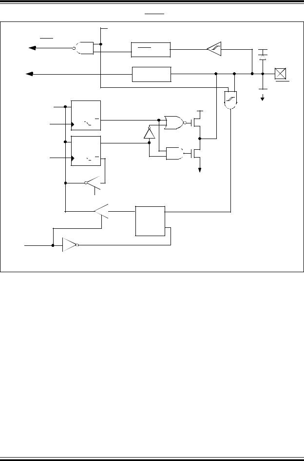
PIC16F62X |
|
|
|
FIGURE 5-5: BLOCK DIAGRAM OF THE RA5/MCLR/THV PIN |
|||
|
|
MCLRE |
|
MCLR circuit |
|
|
|
|
|
|
VDD |
|
|
MCLR Filter(1) |
|
Program mode |
|
|
HV Detect |
|
|
|
|
|
|
|
RA5/MCLR/THV |
Data |
D |
Q |
VSS |
Bus |
VDD |
||
|
|
|
|
WR |
CK |
Q |
P |
PORT |
|
|
|
|
|
|
|
|
Data Latch |
|
|
|
D |
Q |
|
WR |
|
|
N |
TRIS |
|
|
|
CK |
Q |
|
|
|
|
||
|
TRIS Latch |
|
|
|
|
|
VSS |
|
|
RD TRIS |
|
|
|
Q |
D |
|
|
|
EN |
RD Port |
|
|
|
DS40300B-page 30 |
Preliminary |
© 1999 Microchip Technology Inc. |
Loading...