


Microchip Technology Inc PIC16C712-JW, PIC16C716-04-P, PIC16C716-04-SO, PIC16C716-20I-P, PIC16C716-20I-SO Datasheet
...PIC16C712/716
8-Bit CMOS Microcontrollers with A/D Converter and Capture/Compare/PWM
Devices included in this Data Sheet:
• PIC16C712 • PIC16C716
Microcontroller Core Features:
•High-performance RISC CPU
•Only 35 single word instructions to learn
•All single cycle instructions except for program branches which are two cycle
•Operating speed: DC - 20 MHz clock input
DC - 200 ns instruction cycle
Device |
Program |
Data Memory |
|
Memory |
|||
|
|
||
|
|
|
|
PIC16C712 |
1K |
128 |
|
PIC16C716 |
2K |
128 |
•Interrupt capability
(up to 7 internal/external interrupt sources)
•Eight level deep hardware stack
•Direct, indirect and relative addressing modes
•Power-on Reset (POR)
•Power-up Timer (PWRT) and Oscillator Start-up Timer (OST)
•Watchdog Timer (WDT) with its own on-chip RC oscillator for reliable operation
•Brown-out detection circuitry for Brown-out Reset (BOR)
•Programmable code-protection
•Power saving SLEEP mode
•Selectable oscillator options
•Low-power, high-speed CMOS EPROM technology
•Fully static design
•In-Circuit Serial Programming (ICSP)
•Wide operating voltage range: 2.5V to 5.5V
•High Sink/Source Current 25/25 mA
•Commercial, Industrial and Extended temperature ranges
•Low-power consumption:
-< 2 mA @ 5V, 4 MHz
-22.5 A typical @ 3V, 32 kHz
-< 1 A typical standby current
Pin Diagrams
18-pin PDIP, SOIC, Windowed CERDIP
RA2/AN2 |
|
|
|
1 |
|
|
18 |
|
|
|
|
RA1/AN1 |
|
|
|
|
|
|
|
|
|
|
|||||
RA3/AN3/VREF |
|
|
|
2 |
|
|
17 |
|
|
|
|
RA0/AN0 |
|
RA4/T0CKI |
|
|
|
3 |
PIC16C716 |
PIC16C712 |
16 |
|
|
|
|
OSC1/CLKIN |
|
|
|
|
|
||||||||||
MCLR/VPP |
|
|
|
4 |
15 |
|
|
|
|
OSC2/CLKOUT |
|||
VSS |
|
|
|
|
5 |
14 |
|
|
|
|
VDD |
||
RB0/INT |
|
|
|
6 |
13 |
|
|
|
|
RB7 |
|||
RB1/T1OSO/T1CKI |
|
|
|
7 |
12 |
|
|
|
|
RB6 |
|||
RB2/T1OSI |
|
|
|
8 |
11 |
|
|
|
|
RB5 |
|||
|
|
|
|
|
|
|
|
|
|||||
|
|
|
|
||||||||||
RB3/CCP1 |
|
|
|
9 |
|
|
10 |
|
|
|
|
RB4 |
|
|
|
|
|
|
|
|
|
|
|
|
|
|
|
20-pin SSOP
RA2/AN2 |
|
|
|
|
|
1 |
|
|
20 |
|
|
|
|
|
|
RA1/AN1 |
||
RA3/AN3/VREF |
|
|
|
|
|
2 |
|
|
19 |
|
|
|
|
|
|
RA0/AN0 |
||
RA4/T0CKI |
|
|
|
|
|
3 |
PIC16C716 |
PIC16C712 |
18 |
|
|
|
|
|
|
OSC1/CLKIN |
||
MCLR/VPP |
|
|
|
|
|
|
4 |
17 |
|
|
|
|
|
|
OSC2/CLKOUT |
|||
VSS |
|
|
|
|
|
|
5 |
|
|
16 |
|
|
|
|
|
|
VDD |
|
VSS |
|
|
|
|
6 |
|
|
15 |
|
|
|
|
|
|
VDD |
|||
RB0/INT |
|
|
|
|
|
7 |
|
|
14 |
|
|
|
|
|
|
RB7 |
||
RB1/T1OSO/T1CKI |
|
|
|
|
|
8 |
|
|
13 |
|
|
|
|
|
|
RB6 |
||
RB2/T1OSI |
|
|
|
|
|
9 |
|
|
12 |
|
|
|
|
|
|
RB5 |
||
RB3/CCP1 |
|
|
|
|
|
10 |
|
|
11 |
|
|
|
|
|
|
RB4 |
||
Peripheral Features:
•Timer0: 8-bit timer/counter with 8-bit prescaler
•Timer1: 16-bit timer/counter with prescaler can be incremented during sleep via external crystal/clock
•Timer2: 8-bit timer/counter with 8-bit period register, prescaler and postscaler
•Capture, Compare, PWM module
•Capture is 16-bit, max. resolution is 12.5 ns, Compare is 16-bit, max. resolution is 200 ns, PWM maximum resolution is 10-bit
•8-bit multi-channel Analog-to-Digital converter
1999 Microchip Technology Inc.
Preliminary
DS41106A-page 1

PIC16C712/716
Key Features |
|
|
PICmicro™ Mid-Range Reference Manual |
PIC16C712 |
PIC16C716 |
(DS33023) |
|
|
|
|
|
|
|
|
Operating Frequency |
DC - 20 MHz |
DC - 20 MHz |
|
|
|
Resets (and Delays) |
POR, BOR (PWRT, OST) |
POR, BOR (PWRT, OST) |
|
|
|
Program Memory (14-bit words) |
1K |
2K |
|
|
|
Data Memory (bytes) |
128 |
128 |
|
|
|
Interrupts |
7 |
7 |
|
|
|
I/O Ports |
Ports A,B |
Ports A,B |
|
|
|
Timers |
3 |
3 |
|
|
|
Capture/Compare/PWM modules |
1 |
1 |
|
|
|
8-bit Analog-to-Digital Module |
4 input channels |
4 input channels |
|
|
|
PIC16C7XX FAMILY OF DEVICES
|
|
PIC16C710 |
PIC16C71 |
PIC16C711 |
PIC16C712 |
PIC16C715 |
PIC16C716 |
PIC16C72A |
PIC16C73B |
||
|
|
||||||||||
|
|
|
|
|
|
|
|
|
|
|
|
Clock |
Maximum Frequency |
20 |
20 |
20 |
20 |
20 |
20 |
|
|
20 |
20 |
of Operation (MHz) |
|
|
|
|
|
|
|
|
|
|
|
|
|
|
|
|
|
|
|
|
|
|
|
|
|
|
|
|
|
|
|
|
|
|
|
|
EPROM Program |
512 |
1K |
1K |
1K |
2K |
2K |
|
|
2K |
4K |
Memory |
Memory |
|
|
|
|
|
|
|
|
|
|
(x14 words) |
|
|
|
|
|
|
|
|
|
|
|
|
|
|
|
|
|
|
|
|
|
|
|
|
Data Memory (bytes) |
36 |
36 |
68 |
128 |
128 |
128 |
|
|
128 |
192 |
|
|
|
|
|
|
|
|
|
|
|
|
|
Timer Module(s) |
TMR0 |
TMR0 |
TMR0 |
TMR0 |
TMR0 |
TMR0 |
|
|
TMR0 |
TMR0 |
|
|
|
|
|
TMR1 |
|
TMR1 |
|
|
TMR1 |
TMR1 |
|
|
|
|
|
TMR2 |
|
TMR2 |
|
|
TMR2 |
TMR2 |
|
|
|
|
|
|
|
|
|
|
|
|
|
Capture/Compare/ |
— |
— |
— |
1 |
— |
1 |
|
|
1 |
2 |
Peripherals |
PWM Module(s) |
|
|
|
|
|
|
|
|
|
|
|
Serial Port(s) |
— |
— |
— |
— |
— |
— |
SPI/I |
2C |
SPI/I2C, |
|
|
(SPI/I2C, USART) |
|
|
|
|
|
|
|
|
|
USART |
|
A/D Converter (8-bit) |
4 |
4 |
4 |
4 |
4 |
4 |
|
|
5 |
5 |
|
Channels |
|
|
|
|
|
|
|
|
|
|
|
|
|
|
|
|
|
|
|
|
|
|
|
Interrupt Sources |
4 |
4 |
4 |
7 |
4 |
7 |
|
|
8 |
11 |
|
|
|
|
|
|
|
|
|
|
|
|
|
I/O Pins |
13 |
13 |
13 |
13 |
13 |
13 |
|
|
22 |
22 |
|
|
|
|
|
|
|
|
|
|
|
|
|
Voltage Range (Volts) |
2.5-6.0 |
3.0-6.0 |
2.5-6.0 |
2.5-5.5 |
2.5-5.5 |
2.5-5.5 |
|
|
2.5-5.5 |
2.5-5.5 |
|
|
|
|
|
|
|
|
|
|
|
|
Features |
In-Circuit Serial |
Yes |
Yes |
Yes |
Yes |
Yes |
Yes |
|
|
Yes |
Yes |
Programming |
|
|
|
|
|
|
|
|
|
|
|
|
|
|
|
|
|
|
|
|
|
|
|
|
Brown-out Reset |
Yes |
— |
Yes |
Yes |
Yes |
Yes |
|
|
Yes |
Yes |
|
|
|
|
|
|
|
|
|
|
|
|
|
Packages |
18-pin DIP, |
18-pin DIP, |
18-pin DIP, |
18-pin DIP, |
18-pin DIP, |
18-pin DIP, |
|
28-pin SDIP, |
28-pin SDIP, |
|
|
|
SOIC; |
SOIC |
SOIC; |
SOIC; |
SOIC; |
SOIC; |
|
SOIC, SSOP |
SOIC |
|
|
|
20-pin SSOP |
|
20-pin SSOP |
20-pin SSOP |
20-pin SSOP |
20-pin SSOP |
|
|
|
|
|
|
|
|
|
|
|
|
|
|
|
|
DS41106A-page 2 |
Preliminary |
1999 Microchip Technology Inc. |

|
|
PIC16C712/716 |
Table of Contents |
|
|
1.0 |
Device Overview .................................................................................................................................................. |
5 |
2.0 |
Memory Organization .......................................................................................................................................... |
9 |
3.0 |
I/O Ports ............................................................................................................................................................ |
21 |
4.0 |
Timer0 Module ................................................................................................................................................... |
29 |
5.0 |
Timer1 Module ................................................................................................................................................... |
31 |
6.0 |
Timer2 Module ................................................................................................................................................... |
36 |
7.0 |
Capture/Compare/PWM (CCP) Module(s) ........................................................................................................ |
39 |
8.0 |
Analog - to - Digital Converter (A/D) Module ......................................................................................................... |
45 |
9.0 |
Special Features of the CPU ............................................................................................................................. |
51 |
10.0 |
Instruction Set Summary ................................................................................................................................... |
67 |
11.0 |
Development Support ........................................................................................................................................ |
69 |
12.0 |
Electrical Characteristics ................................................................................................................................... |
75 |
13.0 |
DC and AC Characteristics Graphs and Tables ................................................................................................ |
91 |
14.0 |
Packaging Information ....................................................................................................................................... |
93 |
Revision History ........................................................................................................................................................... |
99 |
|
Conversion Considerations .......................................................................................................................................... |
99 |
|
Migration from Base-line to Mid-Range Devices .......................................................................................................... |
99 |
|
Index |
........................................................................................................................................................................... |
101 |
On-Line ..........................................................................................................................................................Support |
105 |
|
Reader .......................................................................................................................................................Response |
106 |
|
PIC16C712/716 ...........................................................................................................Product Identification System |
107 |
|
To Our Valued Customers
Most Current Data Sheet
To obtain the most up-to-date version of this data sheet, please register at our Worldwide Web site at:
http://www.microchip.com
You can determine the version of a data sheet by examining its literature number found on the bottom outside corner of any page. The last character of the literature number is the version number. e.g., DS30000A is version A of document DS30000.
New Customer Notification System
Register on our web site (www.microchip.com/cn) to receive the most current information on our products.
Errata
An errata sheet may exist for current devices, describing minor operational differences (from the data sheet) and recommended workarounds. As device/documentation issues become known to us, we will publish an errata sheet. The errata will specify the revision of silicon and revision of document to which it applies.
To determine if an errata sheet exists for a particular device, please check with one of the following:
•Microchip’s Worldwide Web site; http://www.microchip.com
•Your local Microchip sales office (see last page)
•The Microchip Corporate Literature Center; U.S. FAX: (480) 786-7277
When contacting a sales office or the literature center, please specify which device, revision of silicon and data sheet (include literature number) you are using.
Corrections to this Data Sheet
We constantly strive to improve the quality of all our products and documentation. We have spent a great deal of time to ensure that this document is correct. However, we realize that we may have missed a few things. If you find any information that is missing or appears in error, please:
•Fill out and mail in the reader response form in the back of this data sheet.
•E-mail us at webmaster@microchip.com.
We appreciate your assistance in making this a better document.
1999 Microchip Technology Inc. |
Preliminary |
DS41106A-page 3

PIC16C712/716
NOTES:
DS41106A-page 4 |
Preliminary |
1999 Microchip Technology Inc. |
PIC16C712/716
1.0DEVICE OVERVIEW
This document contains device-specific information. Additional information may be found in the PICmicro™ Mid-Range Reference Manual, (DS33023), which may be obtained from your local Microchip Sales Representative or downloaded from the Microchip website. The Reference Manual should be considered a complementary document to this data sheet, and is highly rec-
ommended reading for a better understanding of the device architecture and operation of the peripheral modules.
There are two devices (PIC16C712, PIC16C716) covered by this datasheet.
Figure 1-1 is the block diagram for both devices. The pinouts are listed in Table 1-1.
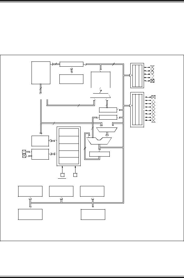
FIGURE 1-1: PIC16C712/716 BLOCK DIAGRAM
13 |
|
Data Bus |
8 |
EPROM |
Program Counter |
|
|
|
|
||
1K X 14 |
|
|
|
or |
|
|
|
2K x 14 |
|
RAM |
|
Program |
8 Level Stack |
|
|
128 x 8 |
|
||
Memory |
(13-bit) |
|
|
|
|
File |
|
|
|
Registers |
|
Program |
14 |
|
|
|
|
|
|
|
RAM Addr(1) |
|
|
|
9 |
||||
Bus |
|
|
|
|||||
|
|
|||||||
|
|
|
|
Addr MUX |
||||
|
|
Instruction reg |
|
|||||
|
|
|
|
|
|
|
|
|
|
|
|
|
|
|
|
|
|
|
|
Direct Addr |
7 |
8 |
Indirect |
|
|
|
|
Addr |
|
|
|
|
|
FSR reg |
|
|
|
8 |
|
STATUS reg |
|
|
|
|
|
|
|
|
|
|
|
3 |
|
|
|
Power-up |
|
MUX |
|
|
|
Timer |
|
|
|
|
Instruction |
Oscillator |
|
|
|
|
Decode & |
Start-up Timer |
|
ALU |
|
|
Control |
|
|
|
|
|
Power-on |
|
|
|
|
|
|
|
8 |
|
|
|
|
Reset |
|
|
|
OSC1/CLKIN |
Timing |
Watchdog |
|
W reg |
|
|
|
|
|||
OSC2/CLKOUT |
Generation |
Timer |
|
|
|
|
|
|
|||
|
|
Brown-out |
|
|
|
|
|
Reset |
|
|
|
|
|
MCLR VDD, VSS |
|
|
|
|
Timer0 |
Timer1 |
|
Timer2 |
|
|
CCP1 |
|
|
A/D |
|
PORTA
RA0/AN0
RA1/AN1
RA2/AN2
RA3/AN3/VREF
RA4/T0CKI
PORTB |
RB0/INT |
RB1/T1OSO/T1CKI |
RB2/T1OSI |
RB3/CCP1 |
RB4 |
RB5 |
RB6 |
RB7 |
Note 1: Higher order bits are from the STATUS register.
1999 Microchip Technology Inc.
Preliminary
DS41106A-page 5

PIC16C712/716
TABLE 1-1 |
PIC16C712/716 PINOUT DESCRIPTION |
|
|
||||||||
|
|
|
Pin |
|
PIC16C712/716 |
Pin |
|
Buffer |
|
||
|
|
|
|
|
|
|
|
|
|
|
|
|
|
|
Name |
|
DIP, SOIC |
SSOP |
Type |
|
Type |
Description |
|
|
|
|
|
|
|
|
|
|
|
|
|
|
MCLR/V |
PP |
|
4 |
4 |
|
|
|
|
||
|
|
MCLR |
|
|
|
|
I |
|
ST |
Master clear (reset) input. This pin is an |
|
|
|
|
|
|
|
|
|
|
|
|
active low reset to the device. |
|
|
VPP |
|
|
|
P |
|
|
Programming voltage input |
||
|
OSC1/CLKIN |
|
16 |
18 |
|
|
|
|
|||
|
|
OSC1 |
|
|
|
I |
|
ST |
Oscillator crystal input or external clock |
||
|
|
|
|
|
|
|
|
|
|
|
source input. ST buffer when configured in |
|
|
|
|
|
|
|
|
|
|
|
RC mode. CMOS otherwise. |
|
|
CLKIN |
|
|
|
I |
|
CMOS |
External clock source input. |
||
|
OSC2/CLKOUT |
|
15 |
17 |
|
|
|
|
|||
|
|
OSC2 |
|
|
|
O |
|
— |
Oscillator crystal output. Connects to |
||
|
|
|
|
|
|
|
|
|
|
|
crystal or resonator in crystal oscillator |
|
|
|
|
|
|
|
|
|
|
|
mode. |
|
|
CLKOUT |
|
|
|
O |
|
— |
In RC mode, OSC2 pin outputs CLKOUT |
||
|
|
|
|
|
|
|
|
|
|
|
which has 1/4 the frequency of OSC1, and |
|
|
|
|
|
|
|
|
|
|
|
denotes the instruction cycle rate. |
|
|
|
|
|
|
|
|
|
|
|
|
|
|
|
|
|
|
|
|
|
|
|
PORTA is a bi-directional I/O port. |
|
RA0/AN0 |
|
17 |
19 |
|
|
|
|
|||
|
|
RA0 |
|
|
|
I/O |
|
TTL |
Digital I/O |
||
|
|
AN0 |
|
|
|
I |
|
Analog |
Analog input 0 |
||
|
RA1/AN1 |
|
18 |
20 |
|
|
|
|
|||
|
|
RA1 |
|
|
|
I/O |
|
TTL |
Digital I/O |
||
|
|
AN1 |
|
|
|
I |
|
Analog |
Analog input 1 |
||
|
RA2/AN2 |
|
1 |
1 |
|
|
|
|
|||
|
|
RA2 |
|
|
|
I/O |
|
TTL |
Digital I/O |
||
|
|
AN2 |
|
|
|
I |
|
Analog |
Analog input 2 |
||
|
RA3/AN3/VREF |
|
2 |
2 |
|
|
|
|
|||
|
|
RA3 |
|
|
|
I/O |
|
TTL |
Digital I/O |
||
|
|
AN3 |
|
|
|
I |
|
Analog |
Analog input 3 |
||
|
|
VREF |
|
|
|
I |
|
Analog |
A/D Reference Voltage input. |
||
|
RA4/T0CKI |
|
3 |
3 |
|
|
|
|
|||
|
|
RA4 |
|
|
|
I/O |
|
ST/OD |
Digital I/O. Open drain when configured |
||
|
|
|
|
|
|
|
|
|
|
|
as output. |
|
|
T0CKI |
|
|
|
I |
|
ST |
Timer0 external clock input |
||
Legend: TTL = TTL-compatible input |
CMOS = CMOS compatible input or output |
ST = Schmitt Trigger input with CMOS levels |
|
OD = Open drain output |
|
SM = SMBus compatible input. An external resistor is required if this pin is used as an output |
|
NPU = N-channel pull-up |
PU = Weak internal pull-up |
No-P diode = No P-diode to VDD |
AN = Analog input or output |
I = input |
O = output |
P = Power |
L = LCD Driver |
DS41106A-page 6 |
Preliminary |
1999 Microchip Technology Inc. |

|
|
|
|
|
|
|
PIC16C712/716 |
|
|
|
|
|
|
|
|
|
|
TABLE 1-1 |
PIC16C712/716 PINOUT DESCRIPTION (Cont.’d) |
|
|
|||||
|
|
|
|
|
|
|
|
|
|
Pin |
|
PIC16C712/716 |
Pin |
Buffer |
|
|
|
|
|
|
|
|
|
|
|
|
|
Name |
|
DIP, SOIC |
SSOP |
Type |
Type |
Description |
|
|
|
|
|
|
|
|
|
|
|
|
|
|
|
|
|
|
|
|
|
|
|
|
|
|
PORTB is a bi-directional I/O port. PORTB |
|
|
|
|
|
|
|
|
can be software programmed for internal |
|
|
|
|
|
|
|
|
weak pull-ups on all inputs. |
|
RB0/INT |
|
6 |
7 |
|
|
|
|
|
|
RB0 |
|
|
|
I/O |
TTL |
Digital I/O |
|
|
INT |
|
|
|
I |
ST |
External Interrupt |
|
RB1/T1OSO/T1CKI |
7 |
8 |
|
|
|
|
||
|
RB1 |
|
|
|
|
|
|
|
|
T1OSO |
|
|
|
I/O |
TTL |
Digital I/O |
|
|
|
|
|
|
O |
— |
Timer1 oscillator output. Connects to |
|
|
T1CKI |
|
|
|
|
|
crystal in oscillator mode. |
|
|
|
|
|
|
I |
ST |
Timer1 external clock input. |
|
RB2/T1OSI |
|
8 |
9 |
|
|
|
|
|
|
RB2 |
|
|
|
I/O |
TTL |
Digital I/O |
|
|
T1OSI |
|
|
|
I |
— |
Timer1 oscillator input. Connects to |
|
|
|
|
|
|
|
|
crystal in oscillator mode. |
|
RB3/CCP1 |
|
9 |
10 |
|
|
|
|
|
|
RB3 |
|
|
|
I/O |
TTL |
Digital I/O |
|
|
CCP1 |
|
|
|
I/O |
ST |
Capture1 input, Compare1 output, PWM1 |
|
|
|
|
|
|
|
|
output. |
|
RB4 |
|
10 |
12 |
I/O |
TTL |
Digital I/O |
||
|
|
|
|
|
|
|
Interrupt on change pin. |
|
RB5 |
|
11 |
12 |
I/O |
TTL |
Digital I/O |
||
|
|
|
|
|
|
|
Interrupt on change pin. |
|
RB6 |
|
12 |
13 |
I/O |
TTL |
Digital I/O |
||
|
|
|
|
|
|
|
Interrupt on change pin. |
|
|
|
|
|
|
I |
ST |
ICSP programming clock. |
|
RB7 |
|
13 |
14 |
I/O |
TTL |
Digital I/O |
||
|
|
|
|
|
|
|
Interrupt on change pin. |
|
|
|
|
|
|
I/O |
ST |
ICSP programming data. |
|
VSS |
|
5 |
5, 6 |
P |
— |
Ground reference for logic and I/O pins. |
||
VDD |
|
14 |
15, 16 |
P |
— |
Positive supply for logic and I/O pins. |
||
Legend: TTL = TTL-compatible input CMOS = CMOS compatible input or output ST = Schmitt Trigger input with CMOS levels
OD = Open drain output
SM = SMBus compatible input. An external resistor is required if this pin is used as an output
NPU = N-channel pull-up |
PU = Weak internal pull-up |
No-P diode = No P-diode to VDD |
AN = Analog input or output |
I = input |
O = output |
P = Power |
L = LCD Driver |
1999 Microchip Technology Inc.
Preliminary
DS41106A-page 7

PIC16C712/716
NOTES:
DS41106A-page 8 |
Preliminary |
1999 Microchip Technology Inc. |
PIC16C712/716
2.0MEMORY ORGANIZATION
There are two memory blocks in each of these PICmicro® microcontroller devices. Each block (Program Memory and Data Memory) has its own bus so that concurrent access can occur.
Additional information on device memory may be found in the PICmicro Mid-Range Reference Manual, (DS33023).
2.1Program Memory Organization
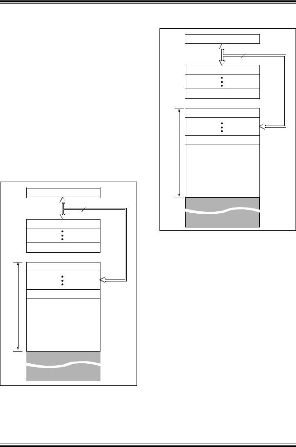
The PIC16C712/716 has a 13-bit program counter capable of addressing an 8K x 14 program memory space. PIC16C712 has 1K x 14 words of program memory and PIC16C716 has 2K x 14 words of program memory. Accessing a location above the physically implemented address will cause a wraparound.
The reset vector is at 0000h and the interrupt vector is at 0004h.
FIGURE 2-1: PROGRAM MEMORY MAP AND STACK OF THE PIC16C712
|
|
PC<12:0> |
|
|
CALL, RETURN |
13 |
|
|
RETFIE, RETLW |
|
|
|
|
|
|
|
Stack Level 1 |
|
|
|
Stack Level 8 |
|
|
|
Reset Vector |
0000h |
|
User Memory |
Interrupt Vector |
0004h |
|
|
|
0005h |
|
On-chip Program |
|
||
Space |
Memory |
|
|
|
|
|
|
|
|
|
03FFh |
|
|
|
0400h |
|
|
|
1FFFh |
FIGURE 2-2: PROGRAM MEMORY MAP AND STACK OF PIC16C716
|
|
PC<12:0> |
|
|
CALL, RETURN |
13 |
|
|
RETFIE, RETLW |
|
|
|
|
|
|
|
Stack Level 1 |
|
|
|
Stack Level 8 |
|
|
|
Reset Vector |
0000h |
|
User Memory |
Interrupt Vector |
0004h |
|
|
|
0005h |
|
On-chip Program |
|
||
Space |
Memory |
|
|
|
|
|
|
|
|
|
07FFh |
|
|
|
0800h |
|
|
|
1FFFh |
1999 Microchip Technology Inc.
Preliminary
DS41106A-page 9

PIC16C712/716
2.2Data Memory Organization
The data memory is partitioned into multiple banks which contain the General Purpose Registers and the Special Function Registers. Bits RP1 and RP0 are the bank select bits.
RP1(1) |
RP0 |
(STATUS<6:5>) |
=00 → Bank0
=01 → Bank1
=10 → Bank2 (not implemented)
=11 → Bank3 (not implemented)
Note 1: Maintain this bit clear to ensure upward compatibility with future products.
Each bank extends up to 7Fh (128 bytes). The lower locations of each bank are reserved for the Special Function Registers. Above the Special Function Registers are General Purpose Registers, implemented as static RAM. All implemented banks contain special function registers. Some “high use” special function registers from one bank may be mirrored in another bank for code reduction and quicker access.
2.2.1GENERAL PURPOSE REGISTER FILE
The register file can be accessed either directly, or indirectly through the File Select Register FSR (Section 2.5).
FIGURE 2-3: REGISTER FILE MAP
File |
|
|
File |
Address |
|
|
Address |
|
|
|
|
00h |
INDF(1) |
INDF(1) |
80h |
01h |
TMR0 |
OPTION_REG |
81h |
|
|
|
|
02h |
PCL |
PCL |
82h |
|
|
|
|
03h |
STATUS |
STATUS |
83h |
|
|
|
|
04h |
FSR |
FSR |
84h |
|
|
|
|
05h |
PORTA |
TRISA |
85h |
|
|
|
|
06h |
PORTB |
TRISB |
86h |
|
|
|
|
07h |
DATACCP |
TRISCCP |
87h |
08h |
|
|
88h |
|
|
||
09h |
|
|
89h |
0Ah |
PCLATH |
PCLATH |
8Ah |
|
|
|
|
0Bh |
INTCON |
INTCON |
8Bh |
|
|
|
|
0Ch |
PIR1 |
PIE1 |
8Ch |
0Dh |
|
|
8Dh |
|
|
||
0Eh |
TMR1L |
PCON |
8Eh |
|
|
|
8Fh |
0Fh |
TRM1H |
|
|
10h |
T1CON |
|
90h |
11h |
TRM2 |
|
91h |
12h |
T2CON |
PR2 |
92h |
13h |
|
|
93h |
|
|
||
14h |
|
|
94h |
15h |
CCPR1L |
|
95h |
16h |
CCPR1H |
|
96h |
17h |
CCP1CON |
|
97h |
18h |
|
|
98h |
19h |
|
|
99h |
1Ah |
|
|
9Ah |
1Bh |
|
|
9Bh |
1Ch |
|
|
9Ch |
1Dh |
|
|
9Dh |
1Eh |
ADRES |
|
9Eh |
1Fh |
ADCON0 |
ADCON1 |
9Fh |
20h |
|
|
|
|
General |
A0h |
|
|
|
Purpose |
|
|
General |
Registers |
BFh |
|
Purpose |
32 Bytes |
|
|
|
||
|
Registers |
|
C0h |
|
|
||
|
96 Bytes |
|
|
|
|
|
|
7Fh |
|
|
FFh |
|
Bank 0 |
Bank 1 |
|

 Unimplemented data memory locations, read as ’0’.
Note 1: Not a physical register.
DS41106A-page 10 |
Preliminary |
1999 Microchip Technology Inc. |
PIC16C712/716
2.2.2SPECIAL FUNCTION REGISTERS
The Special Function Registers are registers used by the CPU and Peripheral Modules for controlling the desired operation of the device. These registers are implemented as static RAM. A list of these registers is give in Table 2-1.
The special function registers can be classified into two sets; core (CPU) and peripheral. Those registers associated with the core functions are described in detail in this section. Those related to the operation of the peripheral features are described in detail in that peripheral feature section.
TABLE 2-1 |
SPECIAL FUNCTION REGISTER SUMMARY |
|
|
|
|
|
|
|
|
|
|
|
||||||||||
|
|
|
|
|
|
|
|
|
|
|
|
|
|
|
|
|
|
|
Value on: |
Value on all |
||
Addr |
Name |
|
Bit 7 |
Bit 6 |
Bit 5 |
Bit 4 |
Bit 3 |
|
Bit 2 |
Bit 1 |
Bit 0 |
POR, |
other resets |
|||||||||
|
|
|
|
|
|
|
|
|
|
|
|
|
|
|
|
|
|
|
BOR |
(4) |
||
|
|
|
|
|
|
|
|
|
|
|
|
|
|
|
|
|
|
|
|
|
|
|
|
|
|
|
|
|
|
|
|
|
|
|
|
|
|
|
|
|
|
|
|
|
|
Bank 0 |
|
|
|
|
|
|
|
|
|
|
|
|
|
|
|
|
|
|
|
|
|
|
|
|
|
|
|
|
|
|
|
|
|
|
|
|
|
||||||||
00h |
INDF(1) |
|
Addressing this location uses contents of FSR to address data memory (not a physical register) |
0000 |
0000 |
0000 |
0000 |
|||||||||||||||
01h |
TMR0 |
|
Timer0 module’s register |
|
|
|
|
|
|
|
|
|
|
|
|
|
xxxx xxxx |
uuuu uuuu |
||||
|
|
|
|
|
|
|
|
|
|
|
|
|
|
|
|
|
|
|||||
02h |
PCL(1) |
|
Program Counter's (PC) Least Significant Byte |
|
|
|
|
|
|
|
|
|
|
0000 |
0000 |
0000 |
0000 |
|||||
03h |
STATUS(1) |
IRP(4) |
RP1(4) |
RP0 |
|
|
|
|
|
|
|
|
Z |
DC |
C |
|
|
|||||
|
TO |
PD |
rr01 1xxx |
rr0q quuu |
||||||||||||||||||
04h |
FSR(1) |
|
Indirect data memory address pointer |
|
|
|
|
|
|
|
|
|
|
xxxx xxxx |
uuuu uuuu |
|||||||
05h |
PORTA(5,6) |
— |
— |
— (7) |
PORTA Data Latch when written: PORTA pins when read |
--xx xxxx |
--xu uuuu |
|||||||||||||||
06h |
PORTB(5,6) |
PORTB Data Latch when written: PORTB pins when read |
|
|
|
|
|
|
|
xxxx xxxx |
uuuu uuuu |
|||||||||||
07h |
DATACCP |
|
— (7) |
— (7) |
— (7) |
— (7) |
— (7) |
|
DCCP |
— (7) |
DT1CK |
xxxx xxxx |
xxxx xuxu |
|||||||||
08h-09h |
— |
|
Unimplemented |
|
|
|
|
|
|
|
|
|
|
|
|
|
|
— |
|
— |
|
|
0Ah |
PCLATH(1,2) |
— |
— |
— |
Write Buffer for the upper 5 bits of the Program Counter |
---0 0000 |
---0 0000 |
|||||||||||||||
0Bh |
INTCON(1) |
GIE |
PEIE |
T0IE |
INTE |
RBIE |
|
T0IF |
INTF |
RBIF |
0000 |
000x |
0000 |
000u |
||||||||
0Ch |
PIR1 |
|
— |
ADIF |
— |
|
— |
— |
CCP1IF |
TMR2IF |
TMR1IF |
-0-- 0000 |
-0-- 0000 |
|||||||||
0Dh |
— |
|
Unimplemented |
|
|
|
|
|
|
|
|
|
|
|
|
|
|
— |
|
— |
|
|
0Eh |
TMR1L |
|
Holding register for the Least Significant Byte of the 16-bit TMR1 register |
|
|
xxxx xxxx |
uuuu uuuu |
|||||||||||||||
|
|
|
|
|
|
|
|
|||||||||||||||
0Fh |
TMR1H |
|
Holding register for the Most Significant Byte of the 16-bit TMR1 register |
|
|
xxxx xxxx |
uuuu uuuu |
|||||||||||||||
|
|
|
|
|
|
|
|
|
|
|
|
|
|
|
|
|
||||||
10h |
T1CON |
|
— |
— |
T1CKPS1 |
T1CKPS0 |
T1OSCEN |
|
|
|
|
|
TMR1CS |
TMR1ON |
|
|
|
|
||||
|
T1SYNC |
--00 0000 |
--uu uuuu |
|||||||||||||||||||
11h |
TMR2 |
|
Timer2 module’s register |
|
|
|
|
|
|
|
|
|
|
|
|
|
0000 0000 |
0000 0000 |
||||
|
|
|
|
|
|
|
|
|
|
|
|
|
|
|
||||||||
12h |
T2CON |
|
— |
TOUTPS3 |
TOUTPS2 |
TOUTPS1 |
TOUTPS0 |
TMR2ON |
T2CKPS1 |
T2CKPS0 |
-000 0000 |
-000 0000 |
||||||||||
13h-14h |
|
|
|
|
|
|
|
|
|
|
|
|
|
|
|
|
|
|
|
|
|
|
15h |
CCPR1L |
|
Capture/Compare/PWM Register1 (LSB) |
|
|
|
|
|
|
|
|
|
|
xxxx xxxx |
uuuu uuuu |
|||||||
|
|
|
|
|
|
|
|
|
|
|
|
|
|
|
|
|||||||
16h |
CCPR1H |
|
Capture/Compare/PWM Register1 (MSB) |
|
|
|
|
|
|
|
|
|
|
xxxx xxxx |
uuuu uuuu |
|||||||
|
|
|
|
|
|
|
|
|
|
|
|
|
|
|||||||||
17h |
CCP1CON |
— |
— |
DC1B1 |
DC1B0 |
CCP1M3 |
CCP1M2 |
CCP1M1 |
CCP1M0 |
--00 0000 |
--00 0000 |
|||||||||||
18h-1Dh |
— |
|
Unimplemented |
|
|
|
|
|
|
|
|
|
|
|
|
|
|
— |
|
— |
|
|
1Eh |
ADRES |
|
A/D Result Register |
|
|
|
|
|
|
|
|
|
|
|
|
|
|
xxxx xxxx |
uuuu uuuu |
|||
|
|
|
|
|
|
|
|
|
|
|
|
|
|
|||||||||
1Fh |
ADCON0 |
|
ADCS1 |
ADCS0 |
CHS2 |
CHS1 |
CHS0 |
|
|
|
— |
ADON |
|
|
||||||||
|
GO/DONE |
0000 00-0 |
0000 00-0 |
|||||||||||||||||||
Legend: |
x = unknown, u = unchanged, q = value depends on condition, - = unimplemented, read as ’0’, |
|
|
|
|
|||||||||||||||||
|
Shaded locations are unimplemented, read as ’0’. |
|
|
|
|
|
|
|
|
|
|
|
|
|
|
|||||||
Note 1: |
These registers can be addressed from either bank. |
|
|
|
|
|
|
|
|
|
|
|
|
|
|
|||||||
2:The upper byte of the program counter is not directly accessible. PCLATH is a holding register for PC<12:8> whose contents are transferred to the upper byte of the program counter.
3:Other (non power-up) resets include: external reset through MCLR and the Watchdog Timer Reset.
4:The IRP and RP1 bits are reserved. Always maintain these bits clear.
5:On any device reset, these pins are configured as inputs.
6:This is the value that will be in the port output latch.
7:Reserved bits; Do Not Use.
1999 Microchip Technology Inc.
Preliminary
DS41106A-page 11

PIC16C712/716
TABLE 2-1 |
SPECIAL FUNCTION REGISTER SUMMARY |
(Cont.’d) |
|
|
|
|
|
|
|
|||||||||||||||
|
|
|
|
|
|
|
|
|
|
|
|
|
|
|
|
|
|
|
|
|
Value on: |
Value on all |
||
Addr |
Name |
|
|
Bit 7 |
|
Bit 6 |
Bit 5 |
Bit 4 |
Bit 3 |
Bit 2 |
|
Bit 1 |
|
Bit 0 |
POR, |
other resets |
||||||||
|
|
|
|
|
|
|
|
|
|
|
|
|
|
|
|
|
|
|
|
|
BOR |
(4) |
||
|
|
|
|
|
|
|
|
|
|
|
|
|
|
|
|
|
|
|
|
|
|
|
|
|
|
|
|
|
|
|
|
|
|
|
|
|
|
|
|
|
|
|
|
|
|
|
|
|
|
Bank 1 |
|
|
|
|
|
|
|
|
|
|
|
|
|
|
|
|
|
|
|
|
|
|
|
|
|
|
|
|
|
|
|
|
|
|
|
|
|
|
|
||||||||||
80h |
INDF(1) |
|
Addressing this location uses contents of FSR to address data memory (not a physical register) |
0000 |
0000 |
0000 |
0000 |
|||||||||||||||||
81h |
OPTION_ |
|
|
|
|
INTEDG |
T0CS |
T0SE |
PSA |
PS2 |
|
PS1 |
|
PS0 |
|
|
|
|
||||||
|
|
RBPU |
|
|
|
1111 |
1111 |
1111 |
1111 |
|||||||||||||||
REG |
|
|
|
|
|
|||||||||||||||||||
|
|
|
|
|
|
|
|
|
|
|
|
|
|
|
|
|
|
|
|
|
|
|
|
|
|
|
|
|
|
|
|
|
|
|
|
|
|
|
|
|
|
|
|
|
|
||||
82h |
PCL(1) |
|
Program Counter’s (PC) Least Significant Byte |
|
|
|
|
|
|
|
|
|
|
0000 |
0000 |
0000 |
0000 |
|||||||
83h |
STATUS(1) |
|
IRP(4) |
|
RP1(4) |
RP0 |
|
|
|
|
|
|
Z |
|
DC |
|
C |
|
|
|||||
|
|
|
TO |
PD |
rr01 1xxx |
rr0q quuu |
||||||||||||||||||
84h |
FSR(1) |
|
Indirect data memory address pointer |
|
|
|
|
|
|
|
|
|
|
xxxx xxxx |
uuuu uuuu |
|||||||||
85h |
TRISA |
|
|
— |
|
— |
— (7) |
PORTA Data Direction Register |
|
|
|
|
|
|
--x1 1111 |
--x1 1111 |
||||||||
86h |
TRISB |
|
PORTB Data Direction Register |
|
|
|
|
|
|
|
|
|
|
|
|
|
1111 |
1111 |
1111 |
1111 |
||||
|
|
|
|
|
|
|
|
|
|
|
|
|
|
|
|
|||||||||
87h |
TRISCCP |
|
|
— (7) |
|
— (7) |
— (7) |
— (7) |
— (7) |
TCCP |
|
— (7) |
TT1CK |
xxxx x1x1 |
xxxx x1x1 |
|||||||||
88h-89h |
— |
|
Unimplemented |
|
|
|
|
|
|
|
|
|
|
|
|
|
|
— |
|
— |
|
|||
8Ah |
PCLATH(1,2) |
|
— |
|
— |
— |
Write Buffer for the upper 5 bits of the Program Counter |
---0 0000 |
---0 0000 |
|||||||||||||||
8Bh |
INTCON(1) |
|
GIE |
|
PEIE |
T0IE |
INTE |
RBIE |
T0IF |
INTF |
RBIF |
0000 |
000x |
0000 |
000u |
|||||||||
8Ch |
PIE1 |
|
|
— |
|
ADIE |
— |
|
— |
— |
CCP1IE |
TMR2IE |
TMR1IE |
-0-- -000 |
-0-- -000 |
|||||||||
8Dh |
— |
|
Unimplemented |
|
|
|
|
|
|
|
|
|
|
|
|
|
|
— |
|
— |
|
|||
8Eh |
PCON |
|
|
— |
|
— |
— |
|
— |
|
— |
— |
|
|
|
|
|
|
|
|
|
|
||
|
|
|
|
|
POR |
BOR |
---- --uu |
|||||||||||||||||
8Fh-91h |
— |
|
Unimplemented |
|
|
|
|
|
|
|
|
|
|
|
|
|
|
— |
|
— |
|
|||
92h |
PR2 |
|
Timer2 Period Register |
|
|
|
|
|
|
|
|
|
|
|
|
|
|
1111 |
1111 |
1111 |
1111 |
|||
|
|
|
|
|
|
|
|
|
|
|
|
|
|
|
|
|
|
|
|
|
|
|
||
93h-9Eh |
— |
|
Unimplemented |
|
|
|
|
|
|
|
|
|
|
|
|
|
|
— |
|
— |
|
|||
9Fh |
ADCON1 |
|
|
— |
|
— |
— |
|
— |
|
— |
PCFG2 |
PCFG1 |
PCFG0 |
---- -000 |
---- -000 |
||||||||
Legend: |
x = unknown, u = unchanged, q = value depends on condition, - = unimplemented, read as ’0’, |
|
|
|
|
|||||||||||||||||||
|
Shaded locations are unimplemented, read as ’0’. |
|
|
|
|
|
|
|
|
|
|
|
|
|
|
|||||||||
Note 1: |
These registers can be addressed from either bank. |
|
|
|
|
|
|
|
|
|
|
|
|
|
|
|||||||||
2:The upper byte of the program counter is not directly accessible. PCLATH is a holding register for PC<12:8> whose contents are transferred to the upper byte of the program counter.
3:Other (non power-up) resets include: external reset through MCLR and the Watchdog Timer Reset.
4:The IRP and RP1 bits are reserved. Always maintain these bits clear.
5:On any device reset, these pins are configured as inputs.
6:This is the value that will be in the port output latch.
7:Reserved bits; Do Not Use.
DS41106A-page 12 |
Preliminary |
1999 Microchip Technology Inc. |

PIC16C712/716
2.2.2.1STATUS REGISTER
The STATUS register, shown in Figure 2-4, contains the arithmetic status of the ALU, the RESET status and the bank select bits for data memory.
The STATUS register can be the destination for any instruction, as with any other register. If the STATUS register is the destination for an instruction that affects the Z, DC or C bits, then the write to these three bits is disabled. These bits are set or cleared according to the device logic. Furthermore, the TO and PD bits are not writable. Therefore, the result of an instruction with the STATUS register as destination may be different than intended.
For example, CLRF STATUS will clear the upper-three bits and set the Z bit. This leaves the STATUS register as 000u u1uu (where u = unchanged).
It is recommended, therefore, that only BCF, BSF, SWAPF and MOVWF instructions are used to alter the STATUS register because these instructions do not affect the Z, C or DC bits from the STATUS register. For other instructions, not affecting any status bits, see the "Instruction Set Summary."
Note 1: These devices do not use bits IRP and RP1 (STATUS<7:6>). Maintain these bits clear to ensure upward compatibility with future products.
Note 2: The C and DC bits operate as a borrow and digit borrow bit, respectively, in subtraction. See the SUBLW and SUBWF instructions for examples.
FIGURE 2-4: STATUS REGISTER (ADDRESS 03h, 83h)
R/W-0 |
R/W-0 |
R/W-0 |
R-1 |
R-1 |
R/W-x |
R/W-x |
R/W-x |
|
|
||||
IRP |
RP1 |
RP0 |
|
TO |
|
|
PD |
|
Z |
DC |
C |
|
R = Readable bit |
bit7 |
|
|
|
|
|
|
|
|
|
|
bit0 |
|
W = Writable bit |
|
|
|
|
|
|
|
|
|
|
|
|
|
U = Unimplemented bit, |
|
|
|
|
|
|
|
|
|
|
|
|
|
read as ‘0’ |
|
|
|
|
|
|
|
|
|
|
|
|
|
- n = Value at POR reset |
bit 7: IRP: Register Bank Select bit (used for indirect addressing)
1 = Bank 2, 3 (100h - 1FFh) - not implemented, maintain clear 0 = Bank 0, 1 (00h - FFh) - not implemented, maintain clear
bit |
6-5: RP1:RP0: Register Bank Select bits (used for direct addressing) |
||||||||||||
|
|
01 = Bank 1 (80h - FFh) |
|||||||||||
|
|
00 = Bank 0 (00h - 7Fh) |
|||||||||||
|
|
Each bank is 128 bytes |
|||||||||||
|
|
Note: RP1 = not implemented, maintain clear |
|||||||||||
bit |
4: |
|
: Time-out bit |
||||||||||
TO |
|||||||||||||
|
|
1 |
= After power-up, CLRWDT instruction, or SLEEP instruction |
||||||||||
|
|
0 |
= A WDT time-out occurred |
||||||||||
bit |
3: |
|
: Power-down bit |
||||||||||
PD |
|||||||||||||
|
|
1 |
= After power-up or by the CLRWDT instruction |
||||||||||
|
|
0 |
= By execution of the SLEEP instruction |
||||||||||
bit |
2: |
Z: Zero bit |
|||||||||||
|
|
1 |
= The result of an arithmetic or logic operation is zero |
||||||||||
|
|
0 |
= The result of an arithmetic or logic operation is not zero |
||||||||||
bit |
|
|
|
|
|
|
|
|
|
||||
1: DC: Digit carry/borrow |
bit (ADDWF, ADDLW,SUBLW,SUBWF instructions) (for borrow the polarity is reversed) |
||||||||||||
|
|
1 |
= A carry-out from the 4th low order bit of the result occurred |
||||||||||
|
|
0 |
= No carry-out from the 4th low order bit of the result |
||||||||||
bit |
0: |
|
|
|
bit (ADDWF, ADDLW,SUBLW,SUBWF instructions) |
||||||||
C: Carry/borrow |
|||||||||||||
|
|
1 |
= A carry-out from the most significant bit of the result occurred |
||||||||||
|
|
0 |
= No carry-out from the most significant bit of the result occurred |
||||||||||
|
|
Note: For |
borrow |
the polarity is reversed. A subtraction is executed by adding the two’s complement of the |
|||||||||
|
|
second operand. For rotate (RRF, RLF) instructions, this bit is loaded with either the high or low order bit of |
|||||||||||
|
|
the source register. |
|||||||||||
1999 Microchip Technology Inc.
Preliminary
DS41106A-page 13

PIC16C712/716
2.2.2.2OPTION_REG REGISTER
The OPTION_REG register is a readable and writable |
Note: |
To achieve a 1:1 prescaler assignment for |
|||||||||||||||||||||||
|
|
the TMR0 register, assign the prescaler to |
|||||||||||||||||||||||
register, which contains various control bits to configure |
|
|
|||||||||||||||||||||||
|
|
the Watchdog Timer. |
|||||||||||||||||||||||
the TMR0 prescaler/WDT postscaler (single assign- |
|
|
|||||||||||||||||||||||
|
|
|
|
|
|
|
|||||||||||||||||||
able register known also as the prescaler), the External |
|
|
|
|
|
|
|
||||||||||||||||||
INT Interrupt, TMR0 and the weak pull-ups on PORTB. |
|
|
|
|
|
|
|
||||||||||||||||||
FIGURE 2-5: OPTION_REG REGISTER (ADDRESS 81h) |
|
|
|
|
|
||||||||||||||||||||
|
|
|
|
|
|
|
|
|
|
|
|
|
|
|
|
|
|
|
|
|
|
||||
|
R/W-1 |
|
|
R/W-1 |
|
R/W-1 |
R/W-1 |
R/W-1 |
R/W-1 |
R/W-1 |
R/W-1 |
|
|
|
|
||||||||||
|
|
RBPU |
|
|
INTEDG |
|
T0CS |
|
T0SE |
|
PSA |
PS2 |
|
PS1 |
|
PS0 |
|
R |
= Readable bit |
|
|||||
|
bit7 |
|
|
|
|
|
|
|
|
|
|
|
|
|
|
|
|
|
|
bit0 |
|
W |
= Writable bit |
|
|
|
|
|
|
|
|
|
|
|
|
|
|
|
|
|
|
|
|
|
|
|
|
|
U |
= Unimplemented bit, |
|
|
|
|
|
|
|
|
|
|
|
|
|
|
|
|
|
|
|
|
|
|
|
|
|
read as ‘0’ |
|
|
|
|
|
|
|
|
|
|
|
|
|
|
|
|
|
|
|
|
|
|
|
|
- n = Value at POR reset |
|
|
|
bit 7: |
|
|
|
: PORTB Pull-up Enable bit |
|
|
|
|
|
|
|
|
|
|||||||||||
RBPU |
|
|
|
|
|
|
|
|
|
||||||||||||||||
|
|
|
|
|
1 |
= PORTB pull-ups are disabled |
|
|
|
|
|
|
|
|
|
||||||||||
|
|
|
|
|
0 |
= PORTB pull-ups are enabled by individual port latch values |
|
|
|
|
|
||||||||||||||
|
bit |
6: |
|
INTEDG: Interrupt Edge Select bit |
|
|
|
|
|
|
|
|
|
||||||||||||
|
|
|
|
|
1 |
= Interrupt on rising edge of RB0/INT pin |
|
|
|
|
|
|
|
||||||||||||
|
|
|
|
|
0 |
= Interrupt on falling edge of RB0/INT pin |
|
|
|
|
|
|
|
||||||||||||
|
bit |
5: |
|
T0CS: TMR0 Clock Source Select bit |
|
|
|
|
|
|
|
|
|
||||||||||||
|
|
|
|
|
1 |
= Transition on RA4/T0CKI pin |
|
|
|
|
|
|
|
|
|
||||||||||
|
|
|
|
|
0 |
= Internal instruction cycle clock (CLKOUT) |
|
|
|
|
|
|
|
||||||||||||
|
bit |
4: |
|
T0SE: TMR0 Source Edge Select bit |
|
|
|
|
|
|
|
|
|
||||||||||||
|
|
|
|
|
1 |
= Increment on high-to-low transition on RA4/T0CKI pin |
|
|
|
|
|
||||||||||||||
|
|
|
|
|
0 |
= Increment on low-to-high transition on RA4/T0CKI pin |
|
|
|
|
|
||||||||||||||
|
bit |
3: |
|
PSA: Prescaler Assignment bit |
|
|
|
|
|
|
|
|
|
|
|
||||||||||
|
|
|
|
|
1 |
= Prescaler is assigned to the WDT |
|
|
|
|
|
|
|
|
|
||||||||||
|
|
|
|
|
0 |
= Prescaler is assigned to the Timer0 module |
|
|
|
|
|
|
|
||||||||||||
|
bit |
2-0: |
PS2:PS0: Prescaler Rate Select bits |
|
|
|
|
|
|
|
|
|
|||||||||||||
|
|
|
|
|
|
Bit Value |
|
TMR0 Rate WDT Rate |
|
|
|
|
|
|
|
|
|
||||||||
|
|
|
|
|
|
|
|
|
|
|
|
|
|
|
|
|
|
|
|
|
|
|
|
||
|
|
|
|
|
|
|
000 |
|
1 : 2 |
|
|
1 : 1 |
|
|
|
|
|
|
|
|
|
|
|
||
|
|
|
|
|
|
|
001 |
|
1 : 4 |
|
|
1 : 2 |
|
|
|
|
|
|
|
|
|
|
|
||
|
|
|
|
|
|
|
010 |
|
1 : 8 |
|
|
1 : 4 |
|
|
|
|
|
|
|
|
|
|
|
||
|
|
|
|
|
|
|
011 |
|
1 : 16 |
|
1 : 8 |
|
|
|
|
|
|
|
|
|
|
|
|||
|
|
|
|
|
|
|
100 |
|
1 : 32 |
|
1 : 16 |
|
|
|
|
|
|
|
|
|
|
||||
|
|
|
|
|
|
|
101 |
|
1 : 64 |
|
1 : 32 |
|
|
|
|
|
|
|
|
|
|
||||
|
|
|
|
|
|
|
110 |
|
1 : 128 |
|
1 : 64 |
|
|
|
|
|
|
|
|
|
|
||||
|
|
|
|
|
|
|
111 |
|
1 : 256 |
|
1 : 128 |
|
|
|
|
|
|
|
|
|
|
||||
|
|
|
|
|
|
|
|
|
|
|
|
|
|
|
|
|
|
|
|
|
|
|
|
|
|
DS41106A-page 14 |
Preliminary |
1999 Microchip Technology Inc. |

PIC16C712/716
2.2.2.3INTCON REGISTER
The INTCON Register is a readable and writable regis- |
Note: |
Interrupt flag bits get set when an interrupt |
||||||||||||||||
|
condition occurs, regardless of the state of |
|||||||||||||||||
ter which contains various enable and flag bits for the |
|
|||||||||||||||||
|
its corresponding enable bit or the global |
|||||||||||||||||
TMR0 register overflow, RB Port change and External |
|
|||||||||||||||||
|
enable bit, GIE (INTCON<7>). User soft- |
|||||||||||||||||
RB0/INT pin interrupts. |
|
|
|
|
|
|
|
|
||||||||||
|
|
|
|
|
|
|
|
ware should ensure the appropriate inter- |
||||||||||
|
|
|
|
|
|
|
|
|
|
|
|
|
|
|||||
|
|
|
|
|
|
|
|
|
|
|
|
|
|
rupt flag bits are clear prior to enabling an |
||||
|
|
|
|
|
|
|
|
|
|
|
|
|
|
interrupt. |
|
|
|
|
FIGURE 2-6: INTCON REGISTER (ADDRESS 0Bh, 8Bh) |
|
|
|
|
|
|||||||||||||
|
|
|
|
|
|
|
|
|
|
|
|
|
|
|
|
|
|
|
|
R/W-0 |
|
R/W-0 |
R/W-0 |
R/W-0 |
R/W-0 |
R/W-0 |
R/W-0 |
R/W-x |
|
|
|
||||||
|
|
GIE |
|
PEIE |
|
T0IE |
INTE |
|
RBIE |
|
T0IF |
|
INTF |
RBIF |
|
R |
= Readable bit |
|
|
bit7 |
|
|
|
|
|
|
|
|
|
|
|
bit0 |
W |
= Writable bit |
|
||
|
|
|
|
|
|
|
|
|
|
|
|
|
|
|
|
U |
= Unimplemented bit, |
|
|
|
|
|
|
|
|
|
|
|
|
|
|
|
|
|
|
read as ‘0’ |
|
|
|
|
|
|
|
|
|
|
|
|
|
|
|
|
|
- n = Value at POR reset |
|
|
|
bit 7: |
GIE: Global Interrupt Enable bit |
|
|
|
|
|
|
|
|
|
|
||||||
|
|
|
1 |
= Enables all un-masked interrupts |
|
|
|
|
|
|
|
|
||||||
|
|
|
0 |
= Disables all interrupts |
|
|
|
|
|
|
|
|
|
|
||||
|
bit |
6: |
PEIE: Peripheral Interrupt Enable bit |
|
|
|
|
|
|
|
|
|||||||
|
|
|
1 |
= Enables all un-masked peripheral interrupts |
|
|
|
|
|
|
||||||||
|
|
|
0 |
= Disables all peripheral interrupts |
|
|
|
|
|
|
|
|
||||||
|
bit |
5: |
T0IE: TMR0 Overflow Interrupt Enable bit |
|
|
|
|
|
|
|
|
|||||||
|
|
|
1 |
= Enables the TMR0 interrupt |
|
|
|
|
|
|
|
|
|
|
||||
|
|
|
0 |
= Disables the TMR0 interrupt |
|
|
|
|
|
|
|
|
||||||
|
bit |
4: |
IINTE: RB0/INT External Interrupt Enable bit |
|
|
|
|
|
|
|||||||||
|
|
|
1 |
= Enables the RB0/INT external interrupt |
|
|
|
|
|
|
||||||||
|
|
|
0 |
= Disables the RB0/INT external interrupt |
|
|
|
|
|
|
||||||||
|
bit |
3: |
RBIE: RB Port Change Interrupt Enable bit |
|
|
|
|
|
|
|||||||||
|
|
|
1 |
= Enables the RB port change interrupt |
|
|
|
|
|
|
|
|
||||||
|
|
|
0 |
= Disables the RB port change interrupt |
|
|
|
|
|
|
|
|
||||||
|
bit |
2: |
T0IF: TMR0 Overflow Interrupt Flag bit |
|
|
|
|
|
|
|
|
|||||||
|
|
|
1 |
= TMR0 register has overflowed (must be cleared in software) |
|
|
|
|||||||||||
|
|
|
0 |
= TMR0 register did not overflow |
|
|
|
|
|
|
|
|
||||||
|
bit |
1: |
INTF: RB0/INT External Interrupt Flag bit |
|
|
|
|
|
|
|
|
|||||||
|
|
|
1 |
= The RB0/INT external interrupt occurred (must be cleared in software) |
|
|
||||||||||||
|
|
|
0 |
= The RB0/INT external interrupt did not occur |
|
|
|
|
|
|
||||||||
|
bit |
0: |
RBIF: RB Port Change Interrupt Flag bit |
|
|
|
|
|
|
|
|
|||||||
|
|
|
1 |
= At least one of the RB7:RB4 pins changed state (must be cleared in software) |
||||||||||||||
|
|
|
0 |
= None of the RB7:RB4 pins have changed state |
|
|
|
|
|
|
||||||||
|
|
|
|
|
|
|
|
|
|
|
|
|
|
|
|
|
|
|
1999 Microchip Technology Inc.
Preliminary
DS41106A-page 15

PIC16C712/716
2.2.2.4 |
PIE1 REGISTER |
|
|
|
|
|
|
Note: Bit PEIE |
(INTCON<6>) must be set to |
|||||||||
|
|
|
|
|
|
|
|
|
|
|
|
|
||||||
This register contains the individual enable bits for the |
|
enable any peripheral interrupt. |
||||||||||||||||
|
|
|
|
|
|
|||||||||||||
peripheral interrupts. |
|
|
|
|
|
|
|
|
|
|
|
|
|
|||||
FIGURE 2-7: PIE1 REGISTER (ADDRESS 8Ch) |
|
|
|
|
|
|
||||||||||||
|
|
|
|
|
|
|
|
|
|
|
|
|
|
|
|
|
|
|
|
|
U-0 |
|
|
R/W-0 |
U-0 |
U-0 |
R/W-0 |
R/W-0 |
R/W-0 |
R/W-0 |
|
|
|
||||
|
|
— |
|
|
ADIE |
— |
— |
|
— |
|
CCP1IE |
|
TMR2IE |
TMR1IE |
|
R |
= Readable bit |
|
|
bit7 |
|
|
|
|
|
|
|
|
|
|
|
bit0 |
W |
= Writable bit |
|
||
|
|
|
|
|
|
|
|
|
|
|
|
|
|
|
|
U |
= Unimplemented bit, |
|
|
|
|
|
|
|
|
|
|
|
|
|
|
|
|
|
|
read as ‘0’ |
|
|
|
|
|
|
|
|
|
|
|
|
|
|
|
|
|
- n = Value at POR reset |
|
|
|
bit 7: |
|
Unimplemented: Read as ‘0’ |
|
|
|
|
|
|
|
|
|
|
|||||
|
bit |
6: |
|
ADIE: A/D Converter Interrupt Enable bit |
|
|
|
|
|
|
|
|
||||||
|
|
|
1 |
= Enables the A/D interrupt |
|
|
|
|
|
|
|
|
|
|
||||
|
|
|
0 |
= Disables the A/D interrupt |
|
|
|
|
|
|
|
|
|
|
||||
|
bit |
5-3: Unimplemented: Read as ‘0’ |
|
|
|
|
|
|
|
|
|
|
||||||
|
bit |
2: |
|
CCP1IE: CCP1 Interrupt Enable bit |
|
|
|
|
|
|
|
|
||||||
|
|
|
1 |
= Enables the CCP1 interrupt |
|
|
|
|
|
|
|
|
|
|
||||
|
|
|
0 |
= Disables the CCP1 interrupt |
|
|
|
|
|
|
|
|
||||||
|
bit |
1: |
|
TMR2IE: TMR2 to PR2 Match Interrupt Enable bit |
|
|
|
|
|
|
||||||||
|
|
|
1 |
= Enables the TMR2 to PR2 match interrupt |
|
|
|
|
|
|
||||||||
|
|
|
0 |
= Disables the TMR2 to PR2 match interrupt |
|
|
|
|
|
|
||||||||
|
bit |
0: |
|
TMR1IE: TMR1 Overflow Interrupt Enable bit |
|
|
|
|
|
|
||||||||
|
|
|
1 |
= Enables the TMR1 overflow interrupt |
|
|
|
|
|
|
|
|
||||||
|
|
|
0 |
= Disables the TMR1 overflow interrupt |
|
|
|
|
|
|
|
|
||||||
|
|
|
|
|
|
|
|
|
|
|
|
|
|
|
|
|
|
|
DS41106A-page 16 |
Preliminary |
1999 Microchip Technology Inc. |

|
|
|
|
|
|
|
|
|
|
|
|
|
|
|
PIC16C712/716 |
||||
|
|
|
|
|
|
|
|
|
|
|
|
|
|
|
|
|
|
|
|
2.2.2.5 |
PIR1 REGISTER |
|
|
|
|
|
|
|
|
|
|
|
|||||||
|
|
|
|
|
Note: |
Interrupt flag bits get set when an interrupt |
|||||||||||||
|
|
|
|
|
|
|
|
|
|
|
|
|
|
||||||
This register |
contains the individual flag bits for the |
|
condition occurs, regardless of the state of |
||||||||||||||||
peripheral interrupts. |
|
|
|
|
|
|
|
|
its corresponding enable bit or the global |
||||||||||
|
|
|
|
|
|
|
|
|
|
|
|
|
|
|
enable bit, GIE (INTCON<7>). User soft- |
||||
|
|
|
|
|
|
|
|
|
|
|
|
|
|
|
ware should ensure the appropriate inter- |
||||
|
|
|
|
|
|
|
|
|
|
|
|
|
|
|
rupt flag bits are clear prior to enabling an |
||||
|
|
|
|
|
|
|
|
|
|
|
|
|
|
|
interrupt. |
|
|
|
|
FIGURE 2-8: PIR1 REGISTER (ADDRESS 0Ch) |
|
|
|
|
|
|
|||||||||||||
|
|
|
|
|
|
|
|
|
|
|
|
|
|
|
|
|
|
|
|
|
|
U-0 |
|
|
R/W-0 |
U-0 |
U-0 |
R/W-0 |
R/W-0 |
R/W-0 |
R/W-0 |
|
|
|
|||||
|
|
— |
|
|
ADIF |
|
— |
|
— |
|
— |
CCP1IF |
|
TMR2IF |
TMR1IF |
|
R |
= Readable bit |
|
|
bit7 |
|
|
|
|
|
|
|
|
|
|
|
|
bit0 |
W |
= Writable bit |
|
||
|
|
|
|
|
|
|
|
|
|
|
|
|
|
|
|
|
U |
= Unimplemented bit, |
|
|
|
|
|
|
|
|
|
|
|
|
|
|
|
|
|
|
|
read as ‘0’ |
|
|
|
|
|
|
|
|
|
|
|
|
|
|
|
|
|
|
- n = Value at POR reset |
|
|
|
bit 7: |
|
Unimplemented: Read as ‘0’ |
|
|
|
|
|
|
|
|
|
|||||||
|
bit |
6: |
|
ADIF: A/D Converter Interrupt Flag bit |
|
|
|
|
|
|
|
|
|||||||
|
|
|
1 |
= An A/D conversion completed (must be cleared in software) |
|
|
|
||||||||||||
|
|
|
0 |
= The A/D conversion is not complete |
|
|
|
|
|
|
|
|
|||||||
|
bit |
5-3: Unimplemented: Read as ‘0’ |
|
|
|
|
|
|
|
|
|
||||||||
|
bit |
2: |
|
CCP1IF: CCP1 Interrupt Flag bit |
|
|
|
|
|
|
|
|
|||||||
|
|
|
|
Capture Mode |
|
|
|
|
|
|
|
|
|
|
|
||||
|
|
|
1 |
= A TMR1 register capture occurred (must be cleared in software) |
|
|
|
||||||||||||
|
|
|
0 |
= No TMR1 register capture occurred |
|
|
|
|
|
|
|
|
|||||||
|
|
|
|
Compare Mode |
|
|
|
|
|
|
|
|
|
|
|
||||
|
|
|
1 |
= A TMR1 register compare match occurred (must be cleared in software) |
|
|
|||||||||||||
|
|
|
0 |
= No TMR1 register compare match occurred |
|
|
|
|
|
|
|||||||||
|
|
|
|
PWM Mode |
|
|
|
|
|
|
|
|
|
|
|
|
|
||
|
|
|
|
Unused in this mode |
|
|
|
|
|
|
|
|
|
|
|
||||
|
bit |
1: |
|
TMR2IF: TMR2 to PR2 Match Interrupt Flag bit |
|
|
|
|
|
|
|||||||||
|
|
|
1 |
= TMR2 to PR2 match occurred (must be cleared in software) |
|
|
|
||||||||||||
|
|
|
0 |
= No TMR2 to PR2 match occurred |
|
|
|
|
|
|
|
|
|||||||
|
bit |
0: |
|
TMR1IF: TMR1 Overflow Interrupt Flag bit |
|
|
|
|
|
|
|||||||||
|
|
|
1 |
= TMR1 register overflowed (must be cleared in software) |
|
|
|
|
|
||||||||||
|
|
|
0 |
= TMR1 register did not overflow |
|
|
|
|
|
|
|
|
|||||||
|
|
|
|
|
|
|
|
|
|
|
|
|
|
|
|
|
|
|
|
1999 Microchip Technology Inc.
Preliminary
DS41106A-page 17

PIC16C712/716
2.2.2.6 |
PCON REGISTER |
|
|
|
|
|
|
|
Note: |
|
|
|
|
|
|
|
|
|
|
|
|
|
|
|||||||||
|
|
|
|
|
|
|
If the BODEN configuration bit is set, BOR |
|||||||||||||||||||||||||
|
|
|
|
|
|
|
|
|
|
|
|
|
|
|
|
|
||||||||||||||||
The Power Control (PCON) register contains a flag bit |
|
|
|
is ’1’ on Power-on Reset. If the BODEN |
||||||||||||||||||||||||||||
|
|
|
|
|
|
|
|
|
|
|
|
|
|
|
|
|
||||||||||||||||
|
|
|
configuration bit is clear, BOR is unknown |
|||||||||||||||||||||||||||||
to allow differentiation |
between |
a Power-on |
Reset |
|
|
|
||||||||||||||||||||||||||
|
|
|
on Power-on Reset. |
|||||||||||||||||||||||||||||
|
|
|
|
|
|
|
|
|
|
|
|
|
|
|
|
|
|
|
||||||||||||||
(POR) to an external MCLR Reset or WDT Reset. |
|
|
|
|||||||||||||||||||||||||||||
|
|
|
|
|
|
|
|
|
|
|
|
|
|
|
|
|
||||||||||||||||
These devices contain an additional bit to differentiate |
|
|
|
The |
BOR |
|
status bit is a "don't care" and is |
|||||||||||||||||||||||||
a Brown-out Reset condition from a Power-on Reset |
|
|
|
not necessarily predictable if the brown-out |
||||||||||||||||||||||||||||
condition. |
|
|
|
|
|
|
|
|
|
|
|
|
|
|
|
|
circuit is disabled (the BODEN configura- |
|||||||||||||||
|
|
|
|
|
|
|
|
|
|
|
|
|
|
|
|
|
|
|
tion bit is clear). |
BOR |
must then be set by |
|||||||||||
|
|
|
|
|
|
|
|
|
|
|
|
|
|
|
|
|
|
|
the user and checked on subsequent |
|||||||||||||
|
|
|
|
|
|
|
|
|
|
|
|
|
|
|
|
|
|
|
resets to see if it is clear, indicating a |
|||||||||||||
|
|
|
|
|
|
|
|
|
|
|
|
|
|
|
|
|
|
|
brown-out has occurred. |
|||||||||||||
FIGURE 2-9: PCON REGISTER (ADDRESS 8Eh) |
|
|
|
|
|
|
|
|
|
|
|
|
|
|
|
|
|
|||||||||||||||
|
|
|
|
|
|
|
|
|
|
|
|
|
|
|
|
|
|
|
|
|
|
|
|
|
||||||||
|
|
U-0 |
U-0 |
U-0 |
U-0 |
U-0 |
|
U-0 |
R/W-0 |
R/W-q |
|
|
|
|
|
|
|
|
|
|||||||||||||
|
|
— |
— |
|
— |
|
— |
|
— |
|
— |
|
|
|
|
|
|
|
|
|
R |
= Readable bit |
|
|||||||||
|
|
|
|
|
|
|
POR |
BOR |
||||||||||||||||||||||||
|
bit7 |
|
|
|
|
|
|
|
|
|
|
|
|
|
|
|
|
|
bit0 |
|
W |
= Writable bit |
|
|||||||||
|
|
|
|
|
|
|
|
|
|
|
|
|
|
|
|
|
|
|
|
|
|
|
|
|
U |
= Unimplemented bit, |
|
|||||
|
|
|
|
|
|
|
|
|
|
|
|
|
|
|
|
|
|
|
|
|
|
|
|
|
|
read as ‘0’ |
|
|||||
|
|
|
|
|
|
|
|
|
|
|
|
|
|
|
|
|
|
|
|
|
|
|
|
|
- n = Value at POR reset |
|
||||||
|
bit 7-2: |
Unimplemented: Read as ’0’ |
|
|
|
|
|
|
|
|
|
|
|
|
|
|
|
|
|
|
|
|
|
|||||||||
|
bit |
1: |
|
: Power-on Reset Status bit |
|
|
|
|
|
|
|
|
|
|
|
|
|
|
|
|
|
|
|
|
|
|||||||
|
POR |
|
|
|
|
|
|
|
|
|
|
|
|
|
|
|
|
|
|
|
|
|
||||||||||
|
|
|
1 = No Power-on Reset occurred |
|
|
|
|
|
|
|
|
|
|
|
|
|
|
|
|
|
|
|
|
|
||||||||
|
|
|
0 = A Power-on Reset occurred (must be set in software after a Power-on Reset occurs) |
|||||||||||||||||||||||||||||
|
bit |
0: |
|
: Brown-out Reset Status bit |
|
|
|
|
|
|
|
|
|
|
|
|
|
|
|
|
|
|
|
|
||||||||
|
BOR |
|
|
|
|
|
|
|
|
|
|
|
|
|
|
|
|
|
|
|
|
|||||||||||
|
|
|
1 = No Brown-out Reset occurred |
|
|
|
|
|
|
|
|
|
|
|
|
|
|
|
|
|
|
|
|
|||||||||
|
|
|
0 = A Brown-out Reset occurred (must be set in software after a Brown-out Reset occurs) |
|||||||||||||||||||||||||||||
|
|
|
|
|
|
|
|
|
|
|
|
|
|
|
|
|
|
|
|
|
|
|
|
|
|
|
|
|
|
|
|
|
DS41106A-page 18 |
Preliminary |
1999 Microchip Technology Inc. |

PIC16C712/716
2.3PCL and PCLATH
The program counter (PC) specifies the address of the instruction to fetch for execution. The PC is 13 bits wide. The low byte is called the PCL register. This register is readable and writable. The high byte is called the PCH register. This register contains the PC<12:8> bits and is not directly readable or writable. All updates to the PCH register go through the PCLATH register.
2.3.1STACK
The stack allows a combination of up to 8 program calls and interrupts to occur. The stack contains the return address from this branch in program execution.
Midrange devices have an 8 level deep x 13-bit wide hardware stack. The stack space is not part of either program or data space and the stack pointer is not readable or writable. The PC is PUSHed onto the stack when a CALL instruction is executed or an interrupt causes a branch. The stack is POPed in the event of a RETURN, RETLW or a RETFIE instruction execution. PCLATH is not modified when the stack is PUSHed or POPed.
After the stack has been PUSHed eight times, the ninth push overwrites the value that was stored from the first push. The tenth push overwrites the second push (and so on).
2.4Program Memory Paging
The CALL and GOTO instructions provide 11 bits of address to allow branching within any 2K program memory page. When doing a CALL or GOTO instruction, the upper bit of the address is provided by PCLATH<3>. When doing a CALL or GOTO instruction, the user must ensure that the page select bit is programmed so that the desired program memory page is addressed. If a return from a CALL instruction (or interrupt) is executed, the entire 13-bit PC is pushed onto the stack. Therefore, manipulation of the PCLATH<3> bit is not required for the return instructions (which POPs the address from the stack).
1999 Microchip Technology Inc.
Preliminary
DS41106A-page 19
PIC16C712/716
2.5Indirect Addressing, INDF and FSR Registers
The INDF register is not a physical register. Addressing INDF actually addresses the register whose address is contained in the FSR register (FSR is a pointer). This is indirect addressing.
EXAMPLE 2-1: INDIRECT ADDRESSING
•Register file 05 contains the value 10h
•Register file 06 contains the value 0Ah
•Load the value 05 into the FSR register
•A read of the INDF register will return the value of 10h
•Increment the value of the FSR register by one (FSR = 06)
•A read of the INDR register now will return the value of 0Ah.
Reading INDF itself indirectly (FSR = 0) will produce 00h. Writing to the INDF register indirectly results in a no-operation (although STATUS bits may be affected).
FIGURE 2-10: DIRECT/INDIRECT ADDRESSING
A simple program to clear RAM locations 20h-2Fh using indirect addressing is shown in Example 2-2.
EXAMPLE 2-2: HOW TO CLEAR RAM USING INDIRECT ADDRESSING
|
movlw |
0x20 |
;initialize pointer |
|
movwf |
FSR |
; to RAM |
NEXT |
clrf |
INDF |
;clear INDF register |
|
incf |
FSR |
;inc pointer |
|
btfss |
FSR,4 |
;all done? |
|
goto |
NEXT |
;NO, clear next |
CONTINUE |
|
|
|
|
: |
|
;YES, continue |
An effective 9-bit address is obtained by concatenating the 8-bit FSR register and the IRP bit (STATUS<7>), as shown in Figure 2-10. However, IRP is not used in the PIC16C712/716.
|
|
|
|
|
Direct Addressing |
|
|
|
|
|
|
|
|
Indirect Addressing |
|
|||||||||||||||||||
RP1:RP0 |
6 |
|
from opcode |
0 |
|
|
|
|
IRP |
7 |
|
|
FSR register |
0 |
||||||||||||||||||||
|
|
|
|
|
|
|
|
|
|
|
|
|
|
|
|
|
|
|
|
|
|
|
|
|
|
|
|
|
|
|
|
|
|
|
|
(2) |
|
|
|
|
|
|
|
|
|
|
|
|
|
|
|
|
(2) |
|
|
|
|
|
|
|
|
|
|
|
|
|
|||
|
|
|
|
|
|
|
|
|
|
|
|
|
|
|
|
|
|
|
|
|
|
|
|
|
|
|
|
|
|
|||||
bank select |
location select |
|
|
|
|
00 |
|
01 |
10 |
11 |
bank select |
|
|
|
|
location select |
||||||||||||||||||
|
|
|
|
|
|
|
|
|
||||||||||||||||||||||||||
|
|
|
|
|
|
|
|
|
|
|
|
|
|
|
|
|
|
|
|
|
|
|
|
|
|
|
|
|
|
|||||
|
|
|
|
|
|
|
|
|
|
|
|
|
|
|
|
|
|
|
|
|
|
|
|
|
|
|
|
|
||||||
|
|
|
|
|
|
|
|
|
|
|
|
|
|
|
|
|
|
|
|
|
|
|
|
|
|
|
|
|
|
|
|
|
|
|
|
|
|
|
|
|
|
|
|
|
|
|
|
00h |
80h |
100h |
180h |
|
|
|
|
|
|
|
|
|
|
|
|
|
|
||||
|
|
|
|
|
|
|
|
|
|
|
|
|
|
(3) |
(3) |
|
|
|
|
|
|
|
|
|
|
|
|
|
|
|
||||
|
|
|
|
|
|
Data |
|
|
|
|
|
|
|
|
|
|
|
|
|
|
|
|
|
|
|
|
||||||||
|
|
|
|
|
|
Memory(1) |
|
|
|
|
|
|
|
|
|
|
|
|
|
|
|
|
|
|
|
|
|
|
||||||
|
|
|
|
|
|
|
|
|
|
|
|
|
7Fh |
FFh |
17Fh |
1FFh |
|
|
|
|
|
|
|
|
|
|
|
|
|
|
||||
|
|
|
|
|
|
|
|
|
|
|
|
|
|
|
|
|
|
|
|
|
|
|
|
|
|
|
|
|
|
|
|
|
|
|
|
|
|
|
|
|
|
|
|
|
|
|
|
Bank 0 |
Bank 1 |
Bank 2 |
Bank 3 |
|
|
|
|
|
|
|
|
|
|
|
|||||||
Note 1: For register file map detail see Figure 2-3.
2:Maintain clear for upward compatibility with future products.
3:Not implemented.
DS41106A-page 20 |
Preliminary |
1999 Microchip Technology Inc. |
PIC16C712/716
3.0I/O PORTS
Some pins for these I/O ports are multiplexed with an alternate function for the peripheral features on the device. In general, when a peripheral is enabled, that pin may not be used as a general purpose I/O pin.
Additional information on I/O ports may be found in the PICmicro™ Mid-Range Reference Manual, (DS33023).
3.1PORTA and the TRISA Register
PORTA is a 5-bit wide bi-directional port. The corresponding data direction register is TRISA. Setting a TRISA bit (=1) will make the corresponding PORTA pin an input, (i.e., put the corresponding output driver in a hi-impedance mode). Clearing a TRISA bit (=0) will make the corresponding PORTA pin an output, (i.e., put the contents of the output latch on the selected pin).
Reading the PORTA register reads the status of the pins whereas writing to it will write to the port latch. All write operations are read-modify-write operations. Therefore a write to a port implies that the port pins are read, the value is modified, and then written to the port data latch.
Pin RA4 is multiplexed with the Timer0 module clock input to become the RA4/T0CKI pin. The RA4/T0CKI pin is a Schmitt Trigger input and an open drain output. All other RA port pins have TTL input levels and full CMOS output drivers.
PORTA pins, RA3:0, are multiplexed with analog inputs and analog VREF input. The operation of each pin is selected by clearing/setting the control bits in the ADCON1 register (A/D Control Register1).
Note: On a Power-on Reset, these pins are configured as analog inputs and read as '0'.
The TRISA register controls the direction of the RA pins, even when they are being used as analog inputs. The user must ensure the bits in the TRISA register are maintained set when using them as analog inputs.
EXAMPLE 3-1: INITIALIZING PORTA
BCF |
STATUS, RP0 |
; |
CLRF |
PORTA |
; Initialize PORTA by |
|
|
; clearing output |
|
|
; data latches |
BSF |
STATUS, RP0 |
; Select Bank 1 |
MOVLW |
0xEF |
; Value used to |
|
|
; initialize data |
|
|
; direction |
MOVWF |
TRISA |
; Set RA<3:0> as inputs |
|
|
; RA<4> as outputs |
BCF |
STATUS, RP0 |
; Return to Bank 0 |
FIGURE 3-1: BLOCK DIAGRAM OF RA3:RA0
DATA |
D |
Q |
|
|
BUS |
|
|
||
|
|
|
VDD |
VDD |
WR |
|
|
|
|
CK |
Q |
|
|
|
PORT |
P |
|
||
|
|
|
|
|
|
Data Latch |
|
|
|
|
D |
Q |
N |
I/O pin |
WR |
|
|
VSS |
VSS |
TRIS |
CK |
Q |
||
|
|
|
Analog |
|
|
TRIS Latch |
input |
|
|
|
mode |
|
||
|
|
|
|
|
|
|
RD TRIS |
|
TTL |
|
|
|
|
Input |
|
|
Q |
D |
Buffer |
|
|
|
||
|
|
|
EN |
|
RD PORT |
|
|
|
|
To A/D Converter |
|
|
|
|
1998 Microchip Technology Inc.
Preliminary
DS41106A-page 21

PIC16C712/716
FIGURE 3-2: BLOCK DIAGRAM OF RA4/T0CKI PIN
DATA |
|
D |
Q |
|
|
|
BUS |
|
|
|
|||
WR |
|
CK |
Q |
|
|
|
PORT |
N |
I/O Pin |
||||
|
|
|||||
|
|
|
|
|
||
|
|
Data Latch |
|
|
||
|
|
D |
Q |
VSS VSS |
|
|
|
|
|
|
|
||
WR |
|
CK |
Q |
Schmitt |
|
|
TRIS |
|
|
||||
|
|
|
Trigger |
|
||
|
|
|
|
|
||
|
|
TRIS Latch |
Input |
|
||
|
|
Buffer |
|
|||
|
|
|
|
|
||
|
|
RD TRIS |
|
|
||
|
|
|
Q |
D |
|
|
|
|
|
|
ENEN |
|
|
|
RD PORT |
|
|
|
||
|
|
TMR0 Clock Input |
|
|
||
TABLE 3-1 |
PORTA FUNCTIONS |
|||
|
|
|
|
|
Name |
|
Bit# |
Buffer |
Function |
|
|
|
|
|
|
|
|
|
|
RA0/AN0 |
|
bit0 |
TTL |
Input/output or analog input |
RA1/AN1 |
|
bit1 |
TTL |
Input/output or analog input |
RA2/AN2 |
|
bit2 |
TTL |
Input/output or analog input |
RA3/AN3/VREF |
|
bit3 |
TTL |
Input/output or analog input or VREF |
|
|
|
|
Input/output or external clock input for Timer0 |
RA4/T0CKI |
|
bit4 |
ST |
Output is open drain type |
Legend: TTL = TTL input, ST = Schmitt Trigger input
TABLE 3-2 |
SUMMARY OF REGISTERS ASSOCIATED WITH PORTA |
|
|
||||||||||
|
|
|
|
|
|
|
|
|
|
|
|
|
|
|
|
|
|
|
|
|
|
|
|
|
Value on |
Value on all |
|
Address |
Name |
Bit 7 |
Bit 6 |
Bit 5 |
Bit 4 |
Bit 3 |
Bit 2 |
Bit 1 |
Bit 0 |
POR, |
|||
other resets |
|||||||||||||
|
|
|
|
|
|
|
|
|
|
|
BOR |
||
|
|
|
|
|
|
|
|
|
|
|
|
||
|
|
|
|
|
|
|
|
|
|
|
|
||
|
|
|
|
|
|
|
|
|
|
|
|
|
|
05h |
PORTA |
— |
— |
— (1) |
RA4 |
RA3 |
RA2 |
RA1 |
RA0 |
--xx xxxx |
--xu uuuu |
||
85h |
TRISA |
— |
— |
— (1) |
PORTA Data Direction Register |
|
--11 1111 |
--11 1111 |
|||||
9Fh |
ADCON1 |
— |
— |
— |
— |
— |
PCFG2 |
PCFG1 |
PCFG0 |
---- -000 |
---- -000 |
||
|
|
|
|
|
|
|
|
|
|
|
|
|
|
Legend: x = unknown, u = unchanged, - = unimplemented locations read as '0'. Shaded cells are not used by PORTA.
Note 1: Reserved bits; Do Not Use.
DS41106A-page 22 |
Preliminary |
1998 Microchip Technology Inc. |
PIC16C712/716
3.2PORTB and the TRISB Register
PORTB is an 8-bit wide bi-directional port. The corresponding data direction register is TRISB. Setting a TRISB bit (=1) will make the corresponding PORTB pin an input, (i.e., put the corresponding output driver in a hi-impedance mode). Clearing a TRISB bit (=0) will make the corresponding PORTB pin an output, (i.e., put the contents of the output latch on the selected pin).
EXAMPLE 3-1: INITIALIZING PORTB
BCF |
STATUS, RP0 |
; |
|
CLRF |
PORTB |
; Initialize |
PORTB by |
|
|
; clearing output |
|
|
|
; data latches |
|
BSF |
STATUS, RP0 |
; Select Bank 1 |
|
MOVLW |
0xCF |
; Value used |
to |
|
|
; initialize |
data |
|
|
; direction |
|
MOVWF |
TRISB |
; Set RB<3:0> as inputs |
|
|
|
; RB<5:4> as |
outputs |
|
|
; RB<7:6> as |
inputs |
Each of the PORTB pins has a weak internal pull-up. A single control bit can turn on all the pull-ups. This is performed by clearing bit RBPU (OPTION_REG<7>). The weak pull-up is automatically turned off when the port pin is configured as an output. The pull-ups are disabled on a Power-on Reset.
FIGURE 3-3: BLOCK DIAGRAM OF RB0 PIN
VDD
RBPU(1) |
|
|
P |
weak |
VDD |
|
|
|
pull-up |
|
|
DATA BUS |
Data Latch |
|
|
|
|
D |
Q |
|
|
|
|
|
|
|
|
||
WR PORT |
CK |
|
|
|
I/O |
|
|
|
pin |
||
|
|
|
|
||
|
|
|
|
|
|
|
TRIS Latch |
|
|
|
|
|
D |
Q |
TTL |
VSS |
|
|
|
|
|||
|
|
|
|
|
|
WR TRIS |
|
|
Input |
|
|
CK |
|
Buffer |
|
|
|
|
|
|
|
||
|
RD TRIS |
|
|
|
|
|
|
Q |
D |
|
|
|
RD PORT |
EN |
|
|
|
RB0/INT |
|
|
|
|
|
|
|
Schmitt Trigger |
RD PORT |
|
|
|
|
Buffer |
|
||
|
|
|
|
|
|
Note 1: To enable weak pull-ups, set the appropriate TRIS bit(s) and clear the RBPU bit (OPTION_REG<7>).
1999 Microchip Technology Inc.
Preliminary
DS41106A-page 23

PIC16C712/716
PORTB pins RB3:RB1 are multiplexed with several peripheral functions (Table 3-3). PORTB pins RB3:RB0 have Schmitt Trigger input buffers.
When enabling peripheral functions, care should be taken in defining TRIS bits for each PORTB pin. Some peripherals override the TRIS bit to make a pin an output, while other peripherals override the TRIS bit to make a pin an input. Since the TRIS bit override is in effect while the peripheral is enabled, read-modify- write instructions (BSF, BCF, XORWF) with TRISB as destination should be avoided. The user should refer to the corresponding peripheral section for the correct TRIS bit settings.
Four of PORTB’s pins, RB7:RB4, have an interrupt on change feature. Only pins configured as inputs can cause this interrupt to occur (i.e. any RB7:RB4 pin configured as an output is excluded from the interrupt on change comparison). The input pins, RB7:RB4, are compared with the old value latched on the last read of
PORTB. The “mismatch” outputs of RB7:RB4 are OR’ed together to generate the RB Port Change Interrupt with flag bit RBIF (INTCON<0>).
This interrupt can wake the device from SLEEP. The user, in the interrupt service routine, can clear the interrupt in the following manner:
a)Any read or write of PORTB will end the mismatch condition.
b)Clear flag bit RBIF.
A mismatch condition will continue to set flag bit RBIF. Reading PORTB will end the mismatch condition and allow flag bit RBIF to be cleared.
The interrupt on change feature is recommended for wake-up on key depression operation and operations where PORTB is only used for the interrupt on change feature. Polling of PORTB is not recommended while using the interrupt on change feature.
FIGURE 3-4: BLOCK DIAGRAM OF RB1/T1OSO/T1CKI PIN
|
|
|
RBPU(1) |
|
|
|
|
T1OSCEN |
|
|
|
|
T1CS |
|
DATA BUS |
|
|
|
|
RD |
|
|
|
|
DATACCP |
DATACCP<0> |
|
|
|
|
D |
Q |
VDD |
|
WR |
|
|
weak |
VDD |
DATACCP |
CK |
Q |
P pull-up |
|
|
|
|
|
|
|
TRISCCP<0> |
1 |
|
|
|
D |
Q |
RB1/T1OSO/T1CKI |
|
|
|
|||
WR |
CK |
Q |
0 |
|
|
|
|||
TRISCCP |
|
|
||
|
|
|
|
|
|
PORTB<1> |
1 |
|
|
|
D |
Q |
VSS |
|
|
|
|||
WR |
CK |
Q |
0 |
|
PORTB |
|
|
||
|
|
|
|
|
|
TRISB<1> |
|
|
|
|
D |
Q |
|
|
WR TRISB |
CK |
Q |
|
|
|
|
|
||
T1OSCEN |
|
|
|
|
TMR1CS |
|
|
|
|
|
|
|
1 |
|
|
|
|
TTL Buffer |
|
|
RD PORTB |
|
0 |
|
|
|
|
T1CLKIN |
|
|
|
|
ST |
|
|
|
|
Buffer |
|
Note 1: To enable weak pull-ups, set the appropriate TRIS bit(s) and clear the RBPU bit (OPTION_REG<7>). |
||||
DS41106A-page 24 |
Preliminary |
1999 Microchip Technology Inc. |

PIC16C712/716
FIGURE 3-5: BLOCK DIAGRAM OF RB2/T1OSI PIN
|
RBPU(1) |
VDD |
|
|
|
weak |
|
||
|
T1OSCEN |
P pull-up |
VDD |
|
|
PORTB<2> |
|
|
|
DATA BUS |
D |
Q |
|
RB1/T1OSO/T1CKI |
|
|
|||
WR PORTB |
CK |
Q |
|
|
|
|
|
||
|
TRISB<2> |
|
VSS |
|
|
|
|
||
|
D |
Q |
|
|
WR TRISB |
CK |
Q |
|
|
|
|
|
||
T1OSCEN |
|
|
|
|
RD PORTB |
|
|
TTL Buffer |
|
|
|
|
|
|
Note 1: To enable weak pull-ups, set the appropriate TRIS bit(s) and clear the RBPU bit (OPTION_REG<7>).
FIGURE 3-6: BLOCK DIAGRAM OF RB3/CCP1 PIN |
|
||||
|
|
RBPU(1) |
|
|
|
|
|
CCPON |
|
|
|
DATA BUS |
|
1 |
|
|
CCPIN |
|
|
CCPOUT |
|
|
|
RD |
DATACCP<2> |
|
|
||
|
0 |
|
|
|
|
DATACCP |
CCPON |
|
|
|
|
|
|
|
|
1 |
|
|
D |
Q |
|
0 |
|
|
|
|
|
|
|
WR |
CK |
Q |
|
|
VDD |
DATACCP |
|
|
|
||
|
|
|
|
weak |
|
|
|
|
|
|
|
|
TRISCCP<2> |
|
|
P pull-up VDD |
|
|
D |
Q |
|
|
|
WR |
CK |
Q |
|
1 |
RB3/CCP1 |
TRISCCP |
|
|
|
|
|
CCP |
|
|
|
0 |
|
Output |
|
|
|
|
|
Mode |
PORTB<3> |
|
|
|
|
|
|
|
|
||
|
D |
Q |
|
1 |
VSS |
WR |
CK |
Q |
|
0 |
|
PORTB |
|
|
|
|
|
|
TRISB<3> |
|
|
|
|
|
D |
Q |
|
|
|
WR |
CK |
Q |
|
|
|
TRISB |
|
|
|
||
|
|
|
|
|
|
CCPON |
|
|
|
|
|
|
|
|
|
1 |
|
RD PORTB |
|
|
|
0 |
|
|
|
|
|
TTL Buffer |
Note 1: To enable weak pull-ups, set the appropriate TRIS bit(s) |
|
|
|
|
and clear the RBPU bit (OPTION_REG<7>). |
|
|
|
|
|
|
|
1999 Microchip Technology Inc.
Preliminary
DS41106A-page 25

PIC16C712/716
FIGURE 3-7: BLOCK DIAGRAM OF RB7:RB4 PINS
VDD
RBPU(1) |
|
|
P |
weak |
VDD |
|
|
|
pull-up |
|
|
DATA BUS |
Data Latch |
|
|
|
|
D |
Q |
|
|
|
|
|
|
|
|
||
WR PORT |
|
|
|
|
I/O |
CK |
|
|
|
pin |
|
|
|
|
|
||
|
TRIS Latch |
|
|
|
|
|
D |
Q |
|
|
VSS |
|
|
|
|
|
|
WR TRIS |
CK |
|
TTL |
|
|
|
|
Buffer |
|
|
|
|
|
|
ST |
|
|
|
|
|
|
|
|
|
|
|
|
Buffer |
|
|
RD TRIS |
Latch |
|
|
|
|
|
|
|
|
|
|
|
Q |
D |
|
|
Set RBIF |
RD PORT |
EN |
Q1 |
|
|
|
|
|
|
|
|
From other |
|
Q |
D |
|
|
|
|
RD PORT |
|
||
RB7:RB4 pins |
|
|
|
||
|
|
|
EN |
Q3 |
|
|
|
|
|
|
|
RB7:RB6 in serial programming mode |
|
|
|
||
Note 1: To enable weak pull-ups, set the appropriate TRIS bit(s) and clear the RBPU bit (OPTION_REG<7>).
TABLE 3-3 |
PORTB FUNCTIONS |
||
|
|
|
|
Name |
Bit# |
Buffer |
Function |
|
|
|
|
|
|
|
|
RB0/INT |
bit0 |
TTL/ST(1) |
Input/output pin or external interrupt input. Internal software |
|
|
|
programmable weak pull-up. |
RB1/T1OS0/ |
bit1 |
TTL/ST(1) |
Input/output pin or Timer 1 oscillator output, or Timer 1 clock input. Internal |
T1CKI |
|
|
software programmable weak pull-up. See Timer1 section for detailed |
|
|
|
operation. |
RB2/T1OSI |
bit2 |
TTL/ST(1) |
Input/output pin or Timer 1 oscillator input. Internal software programmable |
|
|
|
weak pull-up. See Timer1 section for detailed operation. |
RB3/CCP1 |
bit3 |
TTL/ST(1) |
Input/output pin or Capture 1 input, or Compare 1 output, or PWM1 output. |
|
|
|
Internal software programmable weak pull-up. See CCP1 section for |
|
|
|
detailed operation. |
RB4 |
bit4 |
TTL |
Input/output pin (with interrupt on change). Internal software programmable |
|
|
|
weak pull-up. |
RB5 |
bit5 |
TTL |
Input/output pin (with interrupt on change). Internal software programmable |
|
|
|
weak pull-up. |
RB6 |
bit6 |
TTL/ST(2) |
Input/output pin (with interrupt on change). Internal software programmable |
|
|
|
weak pull-up. Serial programming clock. |
RB7 |
bit7 |
TTL/ST(2) |
Input/output pin (with interrupt on change). Internal software programmable |
|
|
|
weak pull-up. Serial programming data. |
Legend: TTL = TTL input, ST = Schmitt Trigger input
Note 1: This buffer is a Schmitt Trigger input when configured as the external interrupt or peripheral input. 2: This buffer is a Schmitt Trigger input when used in serial programming mode.
DS41106A-page 26 |
Preliminary |
1999 Microchip Technology Inc. |

PIC16C712/716
TABLE 3-4 |
SUMMARY OF REGISTERS ASSOCIATED WITH PORTB |
|
|
|
|
|||||||||||
|
|
|
|
|
|
|
|
|
|
|
|
|
|
|
|
|
|
|
|
|
|
|
|
|
|
|
|
|
|
Value on: |
Value on all |
||
Address |
Name |
|
|
Bit 7 |
|
Bit 6 |
Bit 5 |
Bit 4 |
Bit 3 |
Bit 2 |
Bit 1 |
Bit 0 |
POR, |
|||
|
|
|
other resets |
|||||||||||||
|
|
|
|
|
|
|
|
|
|
|
|
|
BOR |
|||
|
|
|
|
|
|
|
|
|
|
|
|
|
|
|
||
|
|
|
|
|
|
|
|
|
|
|
|
|
|
|
||
|
|
|
|
|
|
|
|
|
|
|
|
|
|
|
||
06h |
PORTB |
|
|
RB7 |
|
RB6 |
RB5 |
RB4 |
RB3 |
RB2 |
RB1 |
RB0 |
xxxx xxxx |
uuuu uuuu |
||
|
|
|
|
|
|
|
|
|
|
|
|
|
|
|
||
86h |
TRISB |
|
PORTB Data Direction Register |
|
|
|
|
1111 |
1111 |
1111 |
1111 |
|||||
|
|
|
|
|
|
|
|
|
|
|
|
|
|
|
|
|
81h |
OPTION_REG |
|
|
|
INTEDG |
T0CS |
T0SE |
PSA |
PS2 |
PS1 |
PS0 |
|
|
|
|
|
|
RBPU |
1111 |
1111 |
1111 |
1111 |
|||||||||||
|
|
|
|
|
|
|
|
|
|
|
|
|
|
|
|
|
Legend: x = unknown, u = unchanged. Shaded cells are not used by PORTB.
1999 Microchip Technology Inc.
Preliminary
DS41106A-page 27

PIC16C712/716
NOTES:
DS41106A-page 28 |
Preliminary |
1999 Microchip Technology Inc. |
PIC16C712/716
4.0TIMER0 MODULE
The Timer0 module timer/counter has the following features:
•8-bit timer/counter
•Readable and writable
•Internal or external clock select
•Edge select for external clock
•8-bit software programmable prescaler
•Interrupt on overflow from FFh to 00h
Figure 4-1 is a simplified block diagram of the Timer0 module.
Additional information on timer modules is available in the PICmicro™ Mid-Range Reference Manual, (DS33023).
4.1Timer0 Operation
Timer0 can operate as a timer or as a counter.
Timer mode is selected by clearing bit T0CS (OPTION_REG<5>). In timer mode, the Timer0 module will increment every instruction cycle (without prescaler). If the TMR0 register is written, the increment is inhibited for the following two instruction cycles. The user can work around this by writing an adjusted value to the TMR0 register.
Counter mode is selected by setting bit T0CS (OPTION_REG<5>). In counter mode, Timer0 will increment on every rising or falling edge of pin RA4/T0CKI. The incrementing edge is determined by the Timer0 Source Edge Select bit T0SE (OPTION_REG<4>). Clearing bit T0SE selects the rising edge. Restrictions on the external clock input are discussed below.
When an external clock input is used for Timer0, it must meet certain requirements. The requirements ensure the external clock can be synchronized with the internal phase clock (TOSC). Also, there is a delay in the actual incrementing of Timer0 after synchronization.
Additional information on external clock requirements is available in the PICmicro™ Mid-Range Reference Manual, (DS33023).
4.2Prescaler
An 8-bit counter is available as a prescaler for the Timer0 module or as a postscaler for the Watchdog Timer, respectively (Figure 4-2). For simplicity, this counter is being referred to as “prescaler” throughout this data sheet. Note that there is only one prescaler available, which is mutually exclusively shared between the Timer0 module and the Watchdog Timer. Thus, a prescaler assignment for the Timer0 module means that there is no prescaler for the Watchdog Timer and vice-versa.
The prescaler is not readable or writable.
The PSA and PS2:PS0 bits (OPTION_REG<3:0>) determine the prescaler assignment and prescale ratio.
Clearing bit PSA will assign the prescaler to the Timer0 module. When the prescaler is assigned to the Timer0 module, prescale values of 1:2, 1:4, ..., 1:256 are selectable.
Setting bit PSA will assign the prescaler to the Watchdog Timer (WDT). When the prescaler is assigned to the WDT, prescale values of 1:1, 1:2, ..., 1:128 are selectable.
When assigned to the Timer0 module, all instructions writing to the TMR0 register (e.g. CLRF 1, MOVWF 1, BSF 1,x....etc.) will clear the prescaler. When assigned to WDT, a CLRWDT instruction will clear the prescaler along with the WDT.
Note: Writing to TMR0 when the prescaler is assigned to Timer0 will clear the prescaler count, but will not change the prescaler assignment.
FIGURE 4-1: TIMER0 BLOCK DIAGRAM
|
|
|
|
|
|
|
|
|
|
|
|
|
|
|
|
|
|
|
|
|
|
|
|
Data Bus |
|||||
|
|
FOSC/4 |
|
|
0 |
|
|
|
|
|
|
1 |
PSout |
|
|
|
|
|
8 |
|
|
||||||||
|
|
|
|
|
|
|
|
|
|
|
|
|
|
|
|
|
|||||||||||||
|
|
|
|
|
|
|
|
|
|
|
|
|
|
|
|
|
|
|
|
|
|
|
|
||||||
|
|
|
|
|
|
|
|
|
|
|
|
|
|
|
|
|
|
|
|
Sync with |
|
|
|
|
|
|
|
||
|
|
|
|
|
|
|
|
|
|
|
|
|
|
|
|
|
|
|
|
|
|
|
|
|
|
|
|||
|
|
|
|
|
|
|
|
|
|
|
|
|
|
|
|
|
|
|
|
|
|
|
TMR0 |
|
|
||||
|
|
|
|
|
|
|
|
|
|
1 |
|
|
|
|
|
|
|
|
|
Internal |
|
|
|
||||||
RA4/T0CKI |
|
|
|
|
|
|
|
|
|
|
|
|
Programmable |
0 |
|
clocks |
|
|
|
|
|
|
|
||||||
|
|
|
|
|
|
|
|
|
|
|
|
|
PSout |
|
|||||||||||||||
|
|
|
|
|
|
|
|
|
|
|
|
|
|
|
|||||||||||||||
pin |
|
|
|
|
|
|
|
|
|
|
|
|
Prescaler(2) |
|
|
|
|
|
|
|
|
|
|
|
|
|
|||
|
|
T0SE |
(1) |
|
|
|
|
|
|
|
|
|
|
|
|
|
|
|
|
|
(2 cycle delay) |
|
|
|
|
|
|
|
|
|
|
|
|
|
|
|
|
|
|
|
|
|
|
|
|
|
|
|
|
|
|
|
|
|
|
||||
|
|
|
|
|
|
|
|
|
|
|
|
|
|
|
|
|
|
|
|
|
|
|
|
|
|
|
|
||
|
|
|
|
|
|
|
|
|
|
|
|
|
3 |
|
|
|
|
|
|
|
|
|
|
Set interrupt |
|||||
|
|
|
|
|
|
|
|
|
|
|
|
|
|
|
|
|
|
PSA(1) |
|
|
|
|
|
||||||
|
|
|
|
|
|
|
|
|
|
|
|
|
|
PS2, PS1, PS0(1) |
|
|
|||||||||||||
|
|
|
|
|
|
|
|
|
|
|
|
|
|
|
|
|
|
|
flag bit T0IF |
||||||||||
|
|
|
|
|
|
|
|
|
|
|
|
|
|
||||||||||||||||
|
|
|
|
|
|
|
|
|
T0CS(1) |
|
|
|
|
|
|
|
|
|
on overflow |
||||||||||
Note 1: T0CS, T0SE, PSA, PS2:PS0 (OPTION_REG<5:0>).
2: The prescaler is shared with Watchdog Timer (refer to Figure 4-2 for detailed block diagram).
1999 Microchip Technology Inc.
Preliminary
DS41106A-page 29
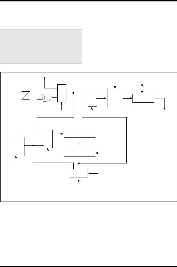
PIC16C712/716
4.2.1SWITCHING PRESCALER ASSIGNMENT
The prescaler assignment is fully under software control, i.e., it can be changed “on the fly” during program execution.
Note: To avoid an unintended device RESET, a specific instruction sequence (shown in the PICmicro™ Mid-Range Reference Manual, DS33023) must be executed when changing the prescaler assignment from Timer0 to the WDT. This sequence must be followed even if the WDT is disabled.
4.3Timer0 Interrupt
The TMR0 interrupt is generated when the TMR0 register overflows from FFh to 00h. This overflow sets bit T0IF (INTCON<2>). The interrupt can be masked by clearing bit T0IE (INTCON<5>). Bit T0IF must be cleared in software by the Timer0 module interrupt service routine before re-enabling this interrupt. The TMR0 interrupt cannot awaken the processor from SLEEP since the timer is shut off during SLEEP.
FIGURE 4-2: BLOCK DIAGRAM OF THE TIMER0/WDT PRESCALER |
|
|||||||
CLKOUT (=Fosc/4) |
|
|
|
|
|
|
|
Data Bus |
|
|
|
0 |
M |
1 |
|
|
8 |
|
|
|
|
|
|
|||
|
|
|
U |
M |
|
|
||
RA4/T0CKI |
|
|
|
|
SYNC |
|
||
pin |
|
|
|
X |
|
U |
TMR0 reg |
|
|
|
1 |
0 |
2 |
||||
|
|
|
||||||
|
|
|
|
X |
Cycles |
|
||
|
|
|
|
|
|
|
||
|
T0SE |
|
|
T0CS |
|
|
|
|
|
|
|
|
|
PSA |
|
Set flag bit T0IF |
|
|
|
|
|
|
|
|
||
|
|
|
|
|
|
|
|
on Overflow |
|
0 |
M |
|
8-bit Prescaler |
|
|
||
|
|
|
|
|
||||
|
|
|
|
|
|
|
|
|
|
1 |
U |
|
|
|
|
|
|
Watchdog |
X |
|
|
8 |
|
|
|
|
|
|
|
|
|
|
|
||
Timer |
|
|
|
|
|
|
|
|
|
|
|
|
8 - to - 1MUX |
|
PS2:PS0 |
|
|
|
|
PSA |
|
|
|
|
|
|
WDT Enable bit |
|
|
|
0 |
1 |
|
|
|
|
|
|
|
|
|
|
|
|
|
|
|
|
|
M U X |
|
PSA |
|
|
|
|
|
|
WDT |
|
|
|
|
|
|
|
|
Time-out |
|
|
|
Note: T0CS, T0SE, PSA, PS2:PS0 are (OPTION_REG<5:0>). |
|
|
||||||
TABLE 4-1 REGISTERS ASSOCIATED WITH TIMER0
|
|
|
|
|
|
|
|
|
|
|
Value on: |
Value on all |
|||
Address |
Name |
Bit 7 |
Bit 6 |
Bit 5 |
Bit 4 |
Bit 3 |
Bit 2 |
Bit 1 |
Bit 0 |
POR, |
|||||
other resets |
|||||||||||||||
|
|
|
|
|
|
|
|
|
|
|
BOR |
||||
|
|
|
|
|
|
|
|
|
|
|
|
|
|||
|
|
|
|
|
|
|
|
|
|
|
|
||||
|
|
|
|
|
|
|
|
|
|
||||||
01h |
TMR0 |
Timer0 module’s register |
|
|
|
|
|
xxxx xxxx |
uuuu uuuu |
||||||
|
|
|
|
|
|
|
|
|
|
|
|
|
|
|
|
0Bh,8Bh |
INTCON |
GIE |
PEIE |
T0IE |
INTE |
RBIE |
T0IF |
INTF |
RBIF |
0000 |
000x |
0000 |
000u |
||
81h |
OPTION_REG |
|
|
INTEDG |
T0CS |
T0SE |
PSA |
PS2 |
PS1 |
PS0 |
1111 |
1111 |
1111 |
1111 |
|
RBPU |
|||||||||||||||
85h |
TRISA |
— |
— |
— (1) |
Bit 4 |
PORTA Data Direction Register |
--11 |
1111 |
--11 |
1111 |
|||||
Legend: x = unknown, u = unchanged, - = unimplemented locations read as '0'. Shaded cells are not used by Timer0.
Note 1: Reserved bit; Do Not Use.
DS41106A-page 30 |
Preliminary |
1999 Microchip Technology Inc. |
 Loading...