


PIC16C554-04-SO
Microchip Technology Inc PIC16C554-04-SO, PIC16C554-04-SS, PIC16C554-04E-JW, PIC16C554-04E-P, PIC16C554-04E-SO Datasheet
...
1997 Microchip Technology Inc.
Preliminary
DS40143B-page 1
Devices included in this data sheet:
Referred to collectively as PIC16C55X(A).
• PIC16C554 PIC16C554A
PIC16C556A
• PIC16C558 PIC16C558A
High Performance RISC CPU:
• Only 35 instructions to learn
• All single-cycle instructions (200 ns), except for
program branches which are two-cycle
• Operating speed:
- DC - 20 MHz clock input
- DC - 200 ns instruction cycle
• Interrupt capability
• 16 special function hardware registers
• 8-level deep hardware stack
• Direct, Indirect and Relative addressing modes
Peripheral Features:
• 13 I/O pins with individual direction control
• High current sink/source for direct LED drive
• Timer0: 8-bit timer/counter with 8-bit
programmable prescaler
Special Microcontroller Features:
• Power-on Reset (POR)
• Power-up Timer (PWRT) and Oscillator Start-up
Timer (OST)
• Watchdog Timer (WDT) with its own on-chip RC
oscillator for reliable operation
Device Program
Memory
Data
Memory
PIC16C554 512 80
PIC16C554A 512 80
PIC16C556A 1K 80
PIC16C558 2K 128
PIC16C558A 2K 128
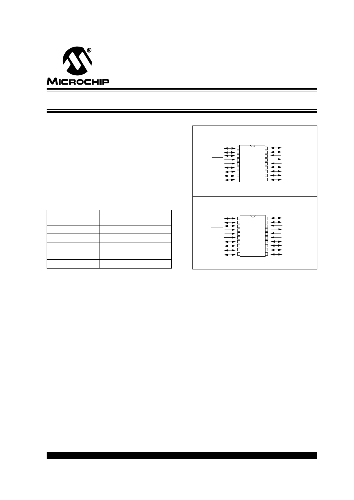
Pin Diagram
Special Microcontroller Features (cont’d)
• Programmable code protection
• Power saving SLEEP mode
• Selectable oscillator options
• Serial in-circuit programming (via two pins)
• Four user programmable ID locations
CMOS Tec hnology:
• Low-power, high-speed CMOS EPROM technology
• Fully static design
• Wide operating voltage range
- 2.5V to 5.5V PIC16C55X
- 3.0 to 5.5V PIC16C55XA
• Commercial, industrial and extended tempera-
ture range
• Low power consumption
- < 2.0 mA @ 5.0V, 4.0 MHz
- 15
µ
A typical @ 3.0V, 32 kHz
- < 1.0
µ
A typical standby current @ 3.0V
RA1
RA0
OSC2/CLKOUT
V
DD
RB7
RB6
RB5
RB4
OSC1/CLKIN
RA2
RA3
MCLR
VSS
RB0/INT
RB1
RB2
RB3
RA4/T0CKI
RA1
RA0
OSC2/CLKOUT
V
DD
RB7
RB6
RB5
RB4
OSC1/CLKIN
RA2
RA3
MCLR
VSS
VSS
RB0/INT
RB1
RB2
RA4/T0CKI
PIC16C55X(A)
RB3RB3
VDD
PDIP, SOIC, Windowed CERDIP
SSOP
2
3
4
5
6
7
8
9
10
•1
2
3
4
5
6
7
8
9
•1
19
18
16
15
14
13
12
11
17
18
17
15
14
13
12
11
10
16
20
PIC16C55X(A)
EPROM-Based 8-Bit CMOS Microcontroller
PIC16C55X(A)

PIC16C55X(A)
DS40143B-page 2
Preliminary
1997 Microchip Technology Inc.
Device Differences
Note 1:
If you change from this device to another device, please verify oscillator characteristics in your application.
Device
Voltage
Range
Oscillator
Process
Technology
(Microns)
PIC16C554 2.5 - 5.5 See Note 1 0.9
PIC16C554A 3.0 - 5.5 See Note 1 0.7
PIC16C556A 3.0 - 5.5 See Note 1 0.7
PIC16C558 2.5 - 5.5 See Note 1 0.9
PIC16C558A 3.0 - 5.5 See Note 1 0.7

1997 Microchip Technology Inc.
Preliminary
DS40143B-page 3
PIC16C55X(A)
Table of Contents
1.0 General Description......................................................................................................................................................................5
2.0 PIC16C55X(A) Device Varieties...................................................................................................................................................7
3.0 Architectural Overview .................................................................................................................................................................9
4.0 Memory Organization................................................................................................................................................................ 13
5.0 I/O Ports.................................................................................................................................................................................... 23
6.0 Timer0 Module .......................................................................................................................................................................... 29
7.0 Special Features of the CPU..................................................................................................................................................... 35
8.0 Instruction Set Summary........................................................................................................................................................... 51
9.0 Development Support................................................................................................................................................................ 63
10.0 Electrical Specifications............................................................................................................................................................. 67
11.0 Packaging Information............................................................................................................................................................... 79
Appendix A: Enhancements............................................................................................................................................................ 87
Appendix B: Compatibility............................................................................................................................................................... 87
INDEX.................................................................................................................................................................................................. 89
PIC16C55X(A) Product Identification System...................................................................................................................................... 95
To Our Valued Customers
We constantly strive to improve the quality of all our products and documentation. To this end, we recently con-
verted to a new publishing software package which we believe will enhance our entire documentation process and
product. As in any conversion process, information may have accidently been altered or deleted. We have spent an
exceptional amount of time to ensure that these documents are correct. However, we realize that we may have
missed a few things. If you find any information that is missing or appears in error from the previous version of this
data sheet (PIC16C55X(A) Data Sheet, Literature Number DS40143B), please use the reader response form in the
back of this data sheet to inform us. We appreciate your assistance in making this a better document.

PIC16C55X(A)
DS40143B-page 4
Preliminary
1997 Microchip Technology Inc.
NOTES:

1997 Microchip Technology Inc.
Preliminary
DS40143B-page 5
PIC16C55X(A)
1.0 GENERAL DESCRIPTION
The PIC16C55X(A) are 18 and 20-Pin EPROM-based
members of the versatile PIC16CXX family of low-cost,
high-performance, CMOS, fully-static, 8-bit
microcontrollers.
All PICmicro™ microcontrollers employ an advanced
RISC architecture. The PIC16C55X(A) have enhanced
core features, eight-lev el deep stack, and multiple inter-
nal and external interrupt sources. The separate
instruction and data buses of the Harvard architecture
allow a 14-bit wide instruction word with the separate
8-bit wide data. The two-stage instruction pipeline
allows all instructions to execute in a single-cycle,
except for program branches (which require two
cycles). A total of 35 instructions (reduced instruction
set) are available . Additionally , a large register set giv es
some of the architectural innovations used to achie ve a
very high performance.
PIC16C55X(A) microcontrollers typically achieve a 2:1
code compression and a 4:1 speed improvement over
other 8-bit microcontrollers in their class.
The PIC16C554(A) and PIC16C556A have 80 bytes of
RAM. The PIC16C558(A) has 128 bytes of RAM. Each
device has 13 I/O pins and an 8-bit timer/counter with
an 8-bit programmable prescaler.
PIC16C55X(A) devices hav e special features to reduce
external components, thus reducing cost, enhancing
system reliability and reducing power consumption.
There are four oscillator options, of which the single pin
RC oscillator provides a low-cost solution, the LP
oscillator minimizes power consumption, XT is a
standard crystal, and the HS is for High Speed crystals.
The SLEEP (power-down) mode offers power saving.
The user can wake up the chip from SLEEP through
several external and internal interrupts and reset.
A highly reliable Watchdog Timer with its own on-chip
RC oscillator provides protection against software
lock- up.
A UV-erasable CERDIP-packaged version is ideal for
code development while the cost-effective One-Time
Programmable (OTP) version is suitable for production
in any volume.
Table 1-1 shows the features of the PIC16C55X(A)
mid-range microcontroller families.
A simplified block diagram of the PIC16C55X(A) is
shown in Figure 3-1.
The PIC16C55X(A) series fit perfectly in applications
ranging from motor control to low-power remote sen-
sors. The EPROM technology makes customization of
application programs (detection levels, pulse genera-
tion, timers, etc.) extremely fast and convenient. The
small footprint packages make this microcontroller
series perfect for all applications with space limitations.
Low-cost, low-power, high-performance, ease of use
and I/O flexibility make the PIC16C55X(A) very versa-
tile.
1.1 F
amily and Upward Compatibility
Those users familiar with the PIC16C5X family of
microcontrollers will realize that this is an enhanced
version of the PIC16C5X architecture. Please refer to
Appendix A for a detailed list of enhancements. Code
written for PIC16C5X can be easily ported to
PIC16C55X(A) family of devices (Appendix B).
The PIC16C55X(A) f amily fills the niche for users w ant-
ing to migrate up from the PIC16C5X family and not
needing various peripheral features of other members
of the PIC16XX mid-range microcontroller family.
1.2 De
velopment Support
The PIC16C55X(A) family is suppor ted by a full-fea-
tured macro assembler, a software simulator, an in-cir-
cuit emulator, a low-cost de v elopment programmer and
a full-featured programmer. A “C” compiler and fuzzy
logic support tools are also available.
PIC16C55X(A)
DS40143B-page 6
Preliminary
1997 Microchip Technology Inc.
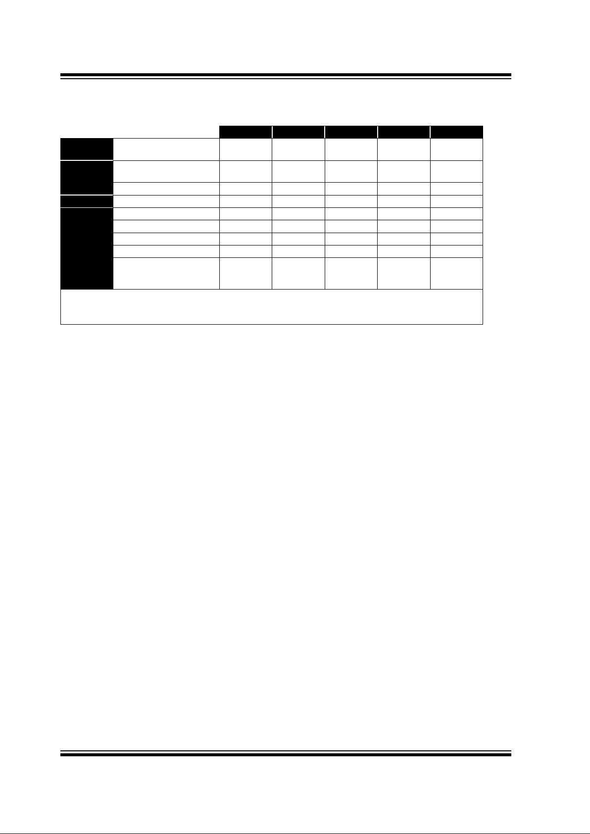
TABLE 1-1: PIC16C55X(A) FAMILY OF DEVICES
PIC16C554
PIC16C554A PIC16C556A PIC16C558 PIC16C558A
Clock
Maximum Frequency of Oper-
ation (MHz)
20 20 20 20 20
Memory
EPROM Program Memory
(x14 words)
512 512 1K 2K 2K
Data Memory (bytes) 80 80 80 128 128
Peripherals
Timer Module(s) TMR0 TMR0 TMR0 TMR0 TMR0
Features
Interrupt Sources 3 3 3 3 3
I/O Pins 13 13 13 13 13
Voltage Range (Volts) 2.5-5.5 3.0-5.5 3.0-5.5 2.5-5.5 3.0-5.5
Brown-out Reset — — — — —
Packages 18-pin DIP,
SOIC;
20-pin SSOP
18-pin DIP,
SOIC;
20-pin SSOP
18-pin DIP,
SOIC;
20-pin SSOP
18-pin DIP,
SOIC;
20-pin SSOP
18-pin DIP,
SOIC;
20-pin SSOP
All PICmicro™ Family devices have Power-on Reset, selectable Watchdog Timer, selectable code protect and high
I/O current capability. All PIC16C55X(A)Family devices use serial programming with clock pin RB6 and data pin RB7.

1997 Microchip Technology Inc.
Preliminary
DS40143B-page 7
PIC16C55X(A)
2.0 PIC16C55X(A) DEVICE
VARIETIES
A variety of frequency ranges and packaging options are
available . Depending on application and production
requirements the proper device option can be selected
using the information in the PIC16C55X(A) Product
Identification System section at the end of this data
sheet. When placing orders, please use this page of the
data sheet to specify the correct part number.
2.1 UV Erasab
le Devices
The UV erasable version, offered in CERDIP package
is optimal for prototype development and pilot
programs. This version can be erased and
reprogrammed to any of the oscillator modes.
Microchip's PICSTART
and PROMATE
programmers both support programming of the
PIC16C55X(A).
2.2 One-Time-Pr
ogrammable (OTP)
Devices
The availability of OTP devices is especially useful for
customers who need the flexibility for frequent code
updates and small volume applications. In addition to
the program memory, the configuration bits must also
be programmed.
2.3 Quic
k-Turnaround-Production (QTP)
Devices
Microchip offers a QTP Programming Service for
factory production orders. This service is made
available for users who choose not to program a
medium to high quantity of units and whose code pat-
terns have stabilized. The devices are identical to the
OTP devices but with all EPROM locations and config-
uration options already programmed by the factory.
Certain code and prototype verification procedures
apply before production shipments are available.
Please contact your Microchip Technology sales office
for more details.
2.4 Serializ
ed
Quick-Turnaround-Production
(SQTP
SM
)
Devices
Microchip offers a unique programming service where
a few user-defined locations in each device are
programmed with different serial numbers. The serial
numbers may be random, pseudo-random or
sequential.
Serial programming allows each device to have a
unique number which can serve as an entry-code,
password or ID number.

PIC16C55X(A)
DS40143B-page 8
Preliminary
1997 Microchip Technology Inc.
NOTES:

1997 Microchip Technology Inc.
Preliminary
DS40143B-page 9
PIC16C55X(A)
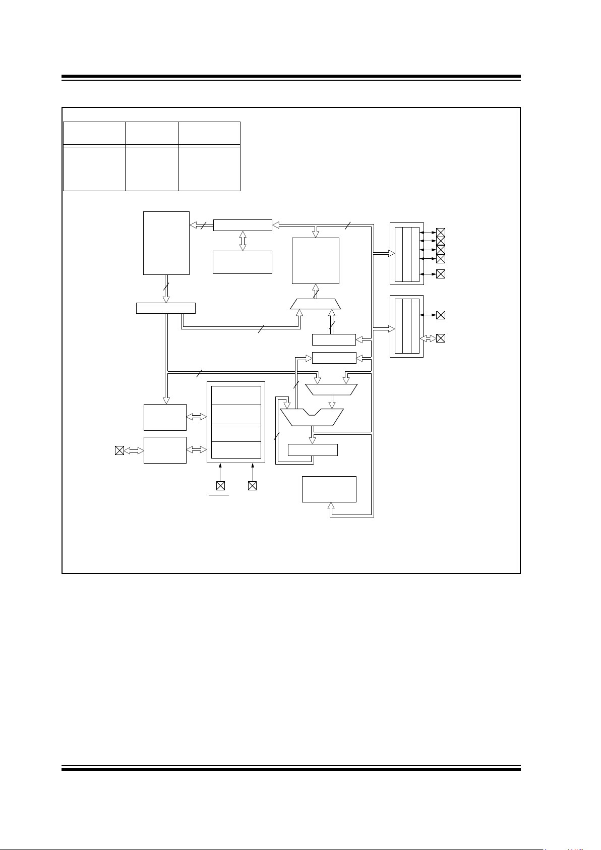
3.0 ARCHITECTURAL OVERVIEW
The high performance of the PIC16C55X(A) family can
be attributed to a number of architectural features
commonly found in RISC microprocessors. To begin
with, the PIC16C55X(A) uses a Harvard architecture,
in which, program and data are accessed from sepa-
rate memories using separate busses. This improves
bandwidth over traditional von Neumann architecture
where program and data are fetched from the same
memory. Separating program and data memory further
allows instructions to be sized differently than 8-bit
wide data words. Instruction opcodes are 14-bits wide
making it possible to have all single word instructions.
A 14-bit wide program memory access bus fetches a
14-bit instruction in a single cycle. A two-stage pipeline
overlaps fetch and execution of instructions.
Consequently, all instructions (35) execute in a sin-
gle-cycle (200 ns @ 20 MHz) except for program
branches.
The PIC16C554(A) addresses 512 x 14 on-chip pro-
gram memory. The PIC16C556A addresses 1K x 14
program memory. The PIC16C558(A) addresses 2K x
14 program memory. All program memory is internal.
The PIC16C55X(A) can directly or indirectly address its
register files or data memory. All special function
registers including the program counter are mapped
into the data memory. The PIC16C55X(A) have an
orthogonal (symmetrical) instruction set that makes it
possible to carry out any operation on any register
using any addressing mode. This symmetrical nature
and lack of ‘special optimal situations’ make program-
ming with the PIC16C55X(A) simple yet efficient. In
addition, the learning curve is reduced significantly.
The PIC16C55X(A) devices contain an 8-bit ALU and
working register. The ALU is a general purpose
arithmetic unit. It performs arithmetic and Boolean
functions between data in the working register and any
register file.
The ALU is 8-bits wide and capable of addition,
subtraction, shift and logical operations. Unless
otherwise mentioned, arithmetic operations are two's
complement in nature. In two-operand instructions,
typically one operand is the working register
(W register). The other operand is a file register or an
immediate constant. In single operand instructions, the
operand is either the W register or a file register.
The W register is an 8-bit working register used for ALU
operations. It is not an addressable register.
Depending on the instruction executed, the ALU may
affect the values of the Carry (C), Digit Carry (DC), and
Zero (Z) bits in the STATUS register. The C and DC bits
operate as a Bo
rrow and Digit Borrow out bit,
respectively, in subtraction. See the
SUBLW
and
SUBWF
instructions for examples.
A simplified block diagram is shown in Figure 3-1, with
a description of the device pins in Table 3-1.
PIC16C55X(A)
DS40143B-page 10
Preliminary
1997 Microchip Technology Inc.
FIGURE 3-1: BLOCK DIAGRAM
Note 1: Higher order bits are from the status register.
Device
Program
Memory
Data Memory
(RAM)
PIC16C554
PIC16C554A
PIC16C556A
PIC16C558
PIC16C558A
512 x 14
512 x 14
1K x 14
2K x 14
2K x 14
80 x 8
80 x 8
80 x 8
128 x 8
128 x 8
EPROM
Program
Memory
2K x 14
13
Data Bus
8
14
Program
Bus
Instruction reg
Program Counter
8 Level Stack
(13-bit)
RAM
File
Registers
128 x 8
Direct Addr
7
8
Addr MUX
Indirect
Addr
8
FSR reg
STATUS reg
MUX
ALU
W reg
Power-up
Timer
Oscillator
Start-up Timer
Power-on
Reset
Watchdog
Timer
Instruction
Decode &
Control
Timing
Generation
OSC1/CLKIN
OSC2/CLKOUT
MCLR
VDD, VSS
Timer0
3
PORTA
PORTB
RA1
RA4/T0CKI
RB0/INT
RB7:RB1
8
8
RAM Addr
(1)
RA0
RA2
RA3
512 x 14
to
80 x 8 to

1997 Microchip Technology Inc.
Preliminary
DS40143B-page 11
PIC16C55X(A)
TABLE 3-1: PIC16C55X(A) PINOUT DESCRIPTION
Name
DIP
SOIC
Pin #
SSOP
Pin #
I/O/P
Type
Buffer
Type
Description
OSC1/CLKIN 16 18 I ST/CMOS Oscillator crystal input/external clock source input.
OSC2/CLKOUT 15 17 O — Oscillator crystal output. Connects to crystal or resonator
in crystal oscillator mode. In RC mode, OSC2 pin outputs
CLKOUT which has 1/4 the frequency of OSC1, and
denotes the instruction cycle rate.
MCLR
/V
PP
4 4 I/P ST Master clear (reset) input/programming voltage input.
This pin is an active low reset to the device.
PORTA is a bi-directional I/O port.
RA0 17 19 I/O ST
RA1 18 20 I/O ST
RA2 1 1 I/O ST
RA3 2 2 I/O ST
RA4/T0CKI 3 3 I/O ST Can be selected to be the clock input to the Timer0
timer/counter. Output is open drain type.
PORTB is a bi-directional I/O port. PORTB can be
software programmed for internal weak pull-up on all
inputs.
RB0/INT 6 7 I/O
TTL/ST
(1)
RB0/INT can also be selected as an external
interrupt pin.
RB1 7 8 I/O TTL
RB2 8 9 I/O TTL
RB3 9 10 I/O TTL
RB4 10 11 I/O TTL Interrupt on change pin.
RB5 11 12 I/O TTL Interrupt on change pin.
RB6 12 13 I/O TTL/ST
(2)
Interrupt on change pin. Serial programming clock.
RB7 13 14 I/O TTL/ST
(2)
Interrupt on change pin. Serial programming data.
V
SS
5 5,6 P — Ground reference for logic and I/O pins.
V
DD
14 15,16 P — Positive supply for logic and I/O pins.
Legend: O = output I/O = input/output P = power
— = Not used I = Input ST = Schmitt Trigger input
TTL = TTL input
Note 1: This buffer is a Schmitt Trigger input when configured as the external interrupt.
Note 2: This buffer is a Schmitt Trigger input when used in serial programming mode.
PIC16C55X(A)
DS40143B-page 12
Preliminary
1997 Microchip Technology Inc.
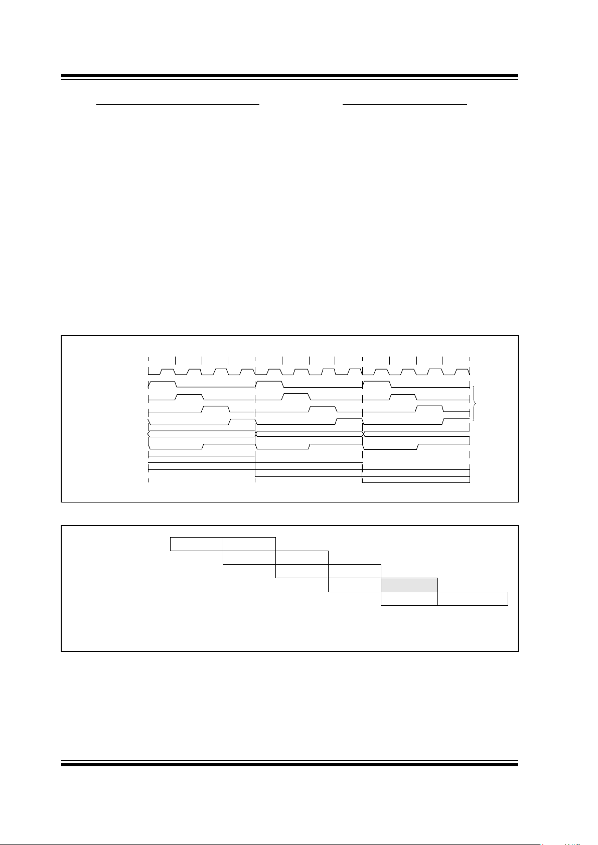
3.1 Cloc
king Scheme/Instruction Cycle
The clock input (OSC1/CLKIN pin) is internally divided
by four to generate four non-overlapping quadrature
clocks namely Q1, Q2, Q3 and Q4. Internally, the
program counter (PC) is incremented every Q1, the
instruction is fetched from the program memory and
latched into the instruction register in Q4. The
instruction is decoded and executed during the
following Q1 through Q4. The clocks and instruction
execution flow are shown in Figure 3-2.
3.2 Instruction Flo
w/Pipelining
An “Instruction Cycle” consists of four Q cycles (Q1,
Q2, Q3 and Q4). The instruction fetch and execute are
pipelined such that fetch takes one instruction cycle
while decode and execute takes another instruction
cycle. However, due to the pipelining, each instruction
effectively executes in one cycle. If an instruction
causes the program counter to change (e.g.,
GOTO
)
then two cycles are required to complete the instruction
(Example 3-1).
A fetch cycle begins with the program counter (PC)
incrementing in Q1.
In the execution cycle, the f etched instruction is latched
into the “Instruction Register (IR)” in cycle Q1. This
instruction is then decoded and executed during the
Q2, Q3, and Q4 cycles. Data memory is read during Q2
(operand read) and written during Q4 (destination
write).
FIGURE 3-2: CLOCK/INSTRUCTION CYCLE
EXAMPLE 3-1: INSTRUCTION PIPELINE FLOW
Q1
Q2 Q3 Q4
Q1
Q2 Q3 Q4
Q1
Q2 Q3 Q4
OSC1
Q1
Q2
Q3
Q4
PC
OSC2/CLKOUT
(RC mode)
PC PC+1 PC+2
Fetch INST (PC)
Execute INST (PC-1) Fetch INST (PC+1)
Execute INST (PC) Fetch INST (PC+2)
Execute INST (PC+1)
Internal
phase
clock
All instructions are single cycle, except for any program branches. These take two cycles since the fetch
instruction is “flushed” from the pipeline while the new instruction is being fetched and then executed.
1. MOVLW 55h
Fetch 1 Execute 1
2. MOVWF PORTB
Fetch 2 Execute 2
3. CALL SUB_1
Fetch 3 Execute 3
4. BSF PORTA, BIT3
Fetch 4 Flush
Fetch SUB_1 Execute SUB_1
1997 Microchip Technology Inc.
Preliminary
DS40143B-page 13
PIC16C55X(A)
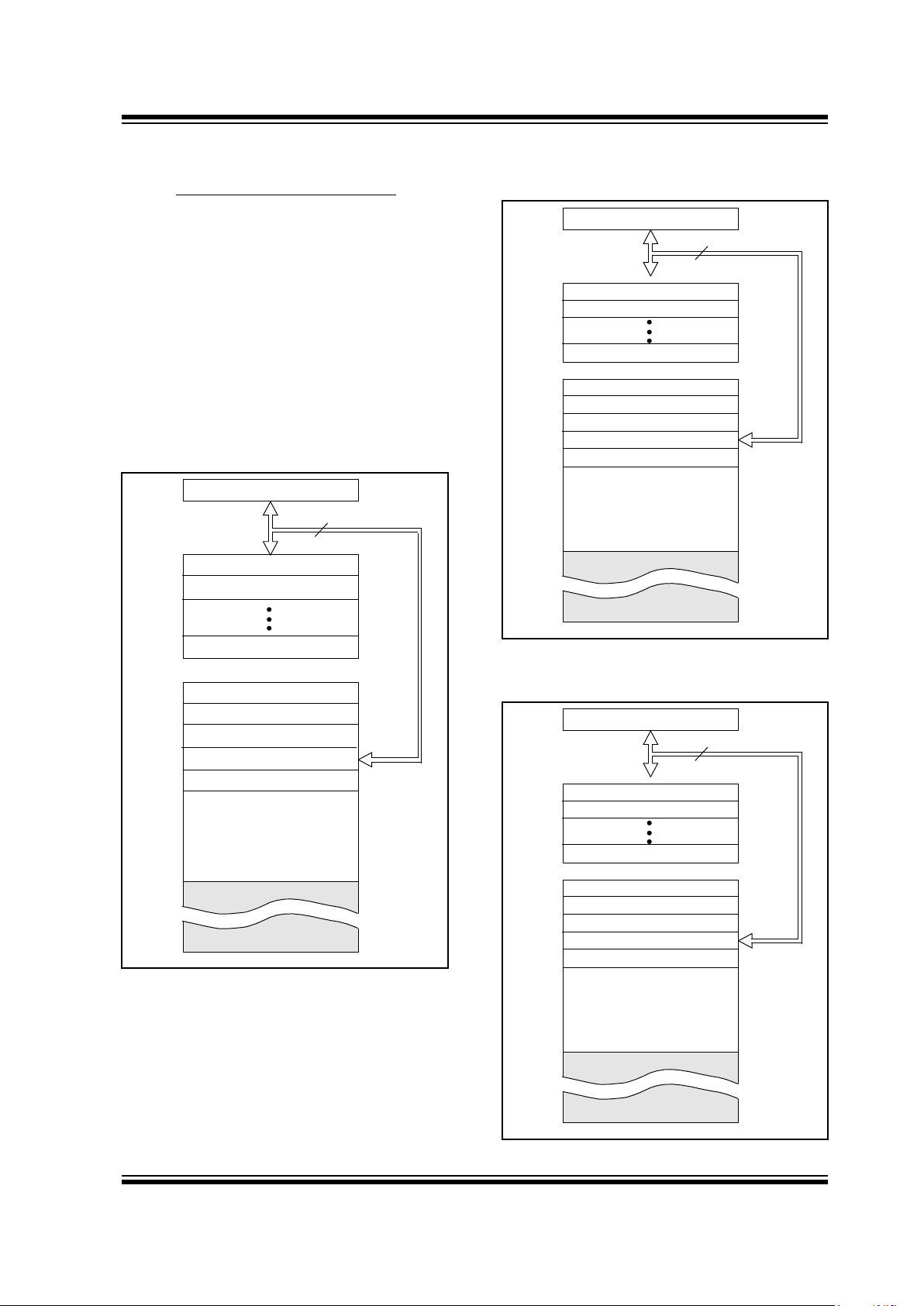
4.0 MEMORY ORGANIZATION
4.1 Pr
ogram Memory Organization
The PIC16C55X(A) has a 13-bit prog ram counter capa-
ble of addressing an 8K x 14 program memory space.
Only the first 512 x 14 (0000h - 01FFh) for the
PIC16C554(A), 1K x 14 (0000h - 03FFh) for the
PIC16C556A and 2K x 14 (0000h - 07FFh) for the
PIC16C558(A) are physically implemented. Accessing
a location above these boundaries will cause a
wrap-around within the first 512 x 14 space
PIC16C554(A) or 1K x 14 space PIC16C556A or 2K x
14 space PIC16C558(A). The reset vector is at 0000h
and the interrupt vector is at 0004h (Figure 4-1,
Figure 4-2, Figure 4-3).
FIGURE 4-1: PROGRAM MEMORY MAP
AND STACK FOR THE
PIC16C554/PIC6C554A
PC<12:0>
13
000h
0004
0005
01FFh
0200h
1FFFh
Stack Level 1
Stack Level 8
Reset Vector
Interrupt Vector
On-chip Program
Memory
CALL, RETURN
RETFIE, RETLW
Stack Level 2
FIGURE 4-2: PROGRAM MEMORY MAP
AND STACK FOR THE
PIC16C556A
FIGURE 4-3: PROGRAM MEMORY MAP
AND STACK FOR THE
PIC16C558/PIC16C558A
PC<12:0>
13
000h
0004
0005
03FFh
0400h
1FFFh
Stack Level 1
Stack Level 8
Reset Vector
Interrupt Vector
On-chip Program
Memory
CALL, RETURN
RETFIE, RETLW
Stack Level 2
PC<12:0>
13
000h
0004
0005
07FFh
0800h
1FFFh
Stack Level 1
Stack Level 8
Reset Vector
Interrupt Vector
On-chip Program
Memory
CALL, RETURN
RETFIE, RETLW
Stack Level 2

PIC16C55X(A)
DS40143B-page 14
Preliminary
1997 Microchip Technology Inc.
4.2 Data Memor
y Organization
The data memory (Figure 4-4 and Figure 4-5) is
partitioned into two Banks which contain the general
purpose registers and the special function registers.
Bank 0 is selected when the RP0 bit is cleared. Bank 1
is selected when the RP0 bit (STATUS <5>) is set. The
Special Function Registers are located in the first 32
locations of each Bank. Register locations 20-6Fh
(Bank0) on the PIC16C554(A)/556A and 20-7Fh
(Bank0) and A0-BFh (Bank1) on the PIC16C558(A) are
general purpose registers implemented as static RAM.
Some special purpose registers are mapped in Bank 1.
4.2.1 GENERAL PURPOSE REGISTER FILE
The register file is organized as 80 x 8 in the
PIC16C554(A)/556A and 128 x 8 in the PIC16C558(A).
Each is accessed either directly or indirectly through
the File Select Register, FSR (Section 4.4).
1997 Microchip Technology Inc. Preliminary DS40143B-page 15
PIC16C55X(A)
FIGURE 4-4: DATA MEMORY MAP FOR
THE PIC16C554(A)/556A
INDF
(1)
TMR0
PCL
STATUS
FSR
PORTA
PORTB
PCLATH
INTCON
INDF
(1)
OPTION
PCL
STATUS
FSR
TRISA
TRISB
PCLATH
INTCON
PCON
00h
01h
02h
03h
04h
05h
06h
07h
08h
09h
0Ah
0Bh
0Ch
0Dh
0Eh
0Fh
10h
11h
12h
13h
14h
15h
16h
17h
18h
19h
1Ah
1Bh
1Ch
1Dh
1Eh
1Fh
80h
81h
82h
83h
84h
85h
86h
87h
88h
89h
8Ah
8Bh
8Ch
8Dh
8Eh
8Fh
90h
91h
92h
93h
94h
95h
96h
97h
98h
99h
9Ah
9Bh
9Ch
9Dh
9Eh
9Fh
20h
A0h
General
Purpose
Register
7Fh
FFh
Bank 0 Bank 1
File
Address
6Fh
70h
Unimplemented data memory locations, read as '0'.
Note 1: Not a physical register.
File
Address
FIGURE 4-5: DATA MEMORY MAP FOR
THE PIC16C558(A)
INDF
(1)
TMR0
PCL
STATUS
FSR
PORTA
PORTB
PCLATH
INTCON
INDF
(1)
OPTION
PCL
STATUS
FSR
TRISA
TRISB
PCLATH
INTCON
PCON
00h
01h
02h
03h
04h
05h
06h
07h
08h
09h
0Ah
0Bh
0Ch
0Dh
0Eh
0Fh
10h
11h
12h
13h
14h
15h
16h
17h
18h
19h
1Ah
1Bh
1Ch
1Dh
1Eh
1Fh
80h
81h
82h
83h
84h
85h
86h
87h
88h
89h
8Ah
8Bh
8Ch
8Dh
8Eh
8Fh
90h
91h
92h
93h
94h
95h
96h
97h
98h
99h
9Ah
9Bh
9Ch
9Dh
9Eh
9Fh
20h
A0h
General
Purpose
Register
7Fh
FFh
Bank 0 Bank 1
File
Address
BFh
C0h
Unimplemented data memory locations, read as '0'.
Note 1: Not a physical register.
File
Address
General
Purpose
Register

PIC16C55X(A)
DS40143B-page 16 Preliminary 1997 Microchip Technology Inc.
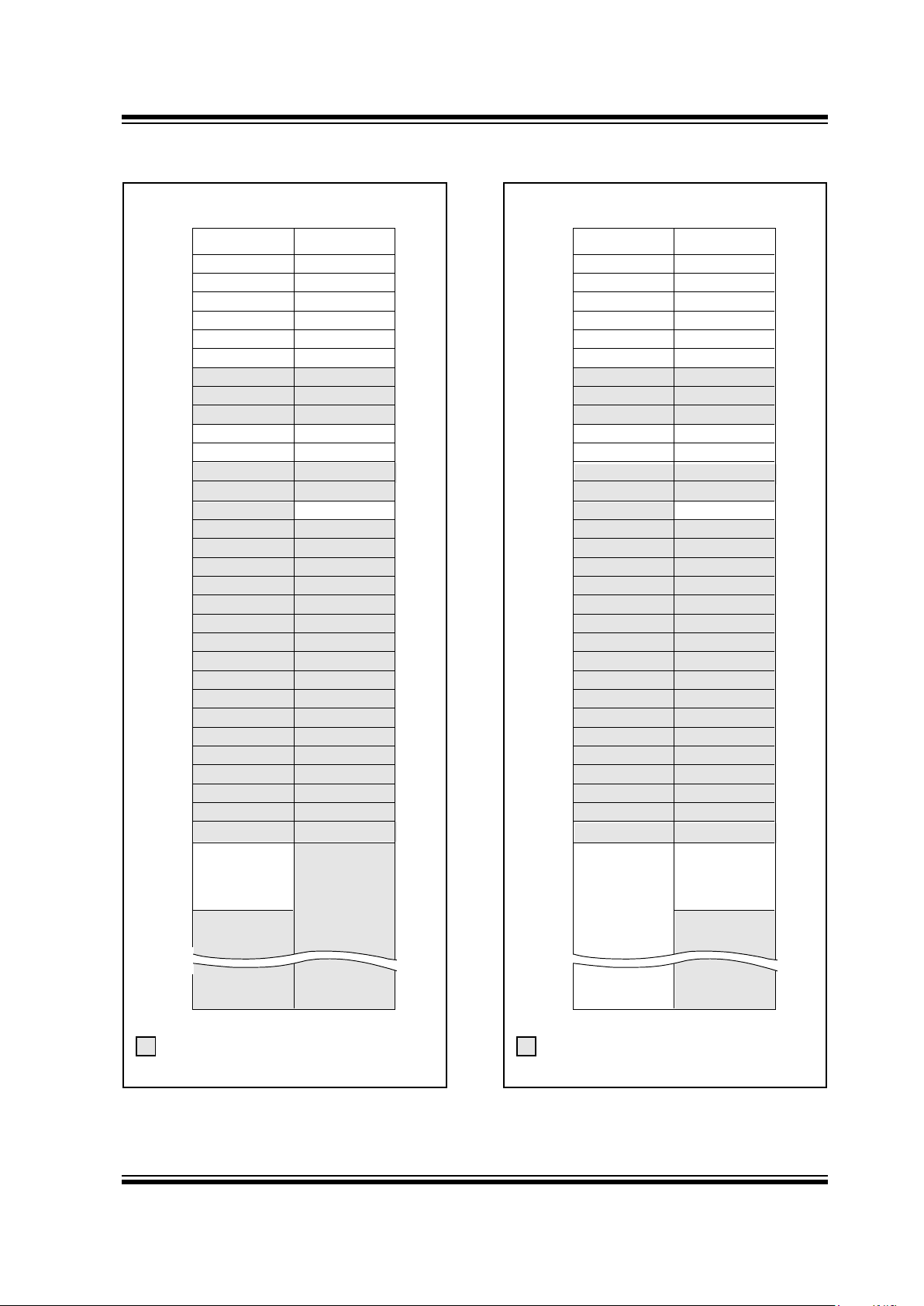
4.2.2 SPECIAL FUNCTION REGISTERS
The special function registers are registers used by the
CPU and Peripheral functions for controlling the
desired operation of the device (Table 4-1). These
registers are static RAM.
The special function registers can be classified into two
sets (core and peripheral). The special function regis-
ters associated with the “core” functions are described
in this section. Those related to the operation of the
peripheral features are described in the section of that
peripheral feature.
TABLE 4-1: SPECIAL REGISTERS FOR THE PIC16C55X(A)
Address Name Bit 7 Bit 6 Bit 5 Bit 4 Bit 3 Bit 2 Bit 1 Bit 0
Value on
POR Reset
Value on
all other
resets
(1)
Bank 0
00h INDF
Addressing this location uses contents of FSR to address data memory (not a physical
register)
xxxx xxxx xxxx xxxx
01h TMR0 Timer0 Module’s Register xxxx xxxx uuuu uuuu
02h PCL Program Counter's (PC) Least Significant Byte 0000 0000 0000 0000
03h STATUS
IRP
(2)
RP1
(2)
RP0 TO PD Z DC C
0001 1xxx 000q quuu
04h FSR Indirect data memory address pointer xxxx xxxx uuuu uuuu
05h PORTA — — — RA4 RA3 RA2 RA1 RA0 ---x xxxx ---u uuuu
06h PORTB RB7 RB6 RB5 RB4 RB3 RB2 RB1 RB0 xxxx xxxx uuuu uuuu
07h Unimplemented — —
08h Unimplemented — —
09h Unimplemented — —
0Ah PCLATH — — — Write buffer for upper 5 bits of program counter ---0 0000 ---0 0000
0Bh INTCON GIE
(3) T0IE INTE RBIE T0IF INTF RBIF 0000 000x 0000 000x
0Ch Unimplemented — —
0Dh-1Eh Unimplemented — —
1Fh Unimplemented — —
Bank 1
80h INDF
Addressing this location uses contents of FSR to address data memory (not a physical
register)
xxxx xxxx xxxx xxxx
81h OPTION RBPU
INTEDG T0CS T0SE PSA PS2 PS1 PS0 1111 1111 1111 1111
82h PCL Program Counter's (PC) Least Significant Byte 0000 0000 0000 0000
83h STATUS
— — RP0 TO PD Z DC C 0001 1xxx 000q quuu
84h FSR Indirect data memory address pointer xxxx xxxx uuuu uuuu
85h TRISA
— — — TRISA4 TRISA3 TRISA2 TRISA1 TRISA0 ---1 1111 ---1 1111
86h TRISB TRISB7 TRISB6 TRISB5 TRISB4 TRISB3 TRISB2 TRISB1 TRISB0 1111 1111 1111 1111
87h Unimplemented — —
88h Unimplemented — —
89h Unimplemented — —
8Ah PCLATH
— — — Write buffer for upper 5 bits of program counter ---0 0000 ---0 0000
8Bh INTCON GIE
(3) T0IE INTE RBIE T0IF INTF RBIF 0000 000x 0000 000x
8Ch Unimplemented — —
8Dh Unimplemented — —
8Eh PCON
— — — — — — POR — ---- --0- ---- --u-
8Fh-9Eh Unimplemented — —
9Fh Unimplemented — —
Legend: — = Unimplemented locations read as ‘0’, u = unchanged, x = unknown, q = value depends on condition,
shaded = unimplemented
Note 1: Other (non power-up) resets include MCLR reset and Watchdog Timer reset during normal operation.
Note 2: IRP & RPI bits are reserved, always maintain these bits clear.
Note 3: Bit 6 of INTCON register is reserved for future use. Always maintain this bit as clear.
1997 Microchip Technology Inc. Preliminary DS40143B-page 17
PIC16C55X(A)
4.2.2.1 STATUS REGISTER
The STATUS register, shown in Figure 4-6, contains
the arithmetic status of the ALU, the RESET status and
the bank select bits for data memory.
The STATUS register can be the destination for any
instruction, like any other register. If the STATUS
register is the destination for an instruction that affects
the Z, DC or C bits, then the write to these three bits is
disabled. These bits are set or cleared according to the
device logic. Furthermore, the T
O and PD bits are not
writable. Therefore, the result of an instruction with the
STATUS register as the destination may be different
than intended.
For example, CLRF STATUS will clear the upper-three
bits and set the Z bit. This lea ves the status register as
000uu1uu (where u = unchanged).
It is recommended, therefore, that only BCF, BSF,
SWAPF and MOVWF instructions be used to alter the ST A-
TUS register because these instructions do not affect
any status bits. For other instructions, not affecting any
status bits, see the “Instruction Set Summary”.
Note 1: The IRP and RP1 bits (STATUS<7:6>)
are not used by the PIC16C55X(A) and
should be programmed as ’0'. Use of
these bits as general purpose R/W bits is
NOT recommended, since this may
affect upward compatibility with future
products.
Note 2: The C and DC bits operate as a Borro
w
and Digit Borrow out bit, respectively, in
subtraction. See the SUBLW and SUBWF
instructions for examples.
FIGURE 4-6: STATUS REGISTER (ADDRESS 03H OR 83H)
Reserved Reserved R/W-0 R-1 R-1 R/W-x R/W-x R/W-x
IRP RP1 RP0 TO PD Z DC C R = Readable bit
W = Writable bit
- n = Value at POR reset
- x = Unknown at POR reset
bit7 bit0
bit 7: IRP: Register Bank Select bit (used for indirect addressing)
1 = Bank 2, 3 (100h - 1FFh)
0 = Bank 0, 1 (00h - FFh)
The IRP bit is reserved on the PIC16C55X(A), always maintain this bit clear.
bit 6-5: RP1:RP0: Register Bank Select bits (used for direct addressing)
11 = Bank 3 (180h - 1FFh)
10 = Bank 2 (100h - 17Fh)
01 = Bank 1 (80h - FFh)
00 = Bank 0 (00h - 7Fh)
Each bank is 128 bytes. The RP1 bit is reserved on the PIC16C55X(A), always maintain this bit clear.
bit 4: T
O: Time-out bit
1 = After power-up, CLRWDT instruction, or SLEEP instruction
0 = A WDT time-out occurred
bit 3: PD
: Power-down bit
1 = After power-up or by the CLRWDT instruction
0 = By execution of the SLEEP instruction
bit 2: Z: Zero bit
1 = The result of an arithmetic or logic operation is zero
0 = The result of an arithmetic or logic operation is not zero
bit 1: DC: Digit carry/borro
w bit (ADDWF, ADDLW,SUBLW,SUBWF instructions)(for borrow the polarity is reversed)
1 = A carry-out from the 4th low order bit of the result occurred
0 = No carry-out from the 4th low order bit of the result
bit 0: C: Carry/borro
w bit (ADDWF, ADDLW,SUBLW,SUBWF instructions)
1 = A carry-out from the most significant bit of the result occurred
0 = No carry-out from the most significant bit of the result occurred
Note: For borro
w the polarity is reversed. A subtraction is executed by adding the two’s complement of the
second operand. For rotate (RRF, RLF) instructions, this bit is loaded with either the high or low order bit of
the source register.

PIC16C55X(A)
DS40143B-page 18 Preliminary 1997 Microchip Technology Inc.
4.2.2.2 OPTION REGISTER
The OPTION register is a readable and writable
register which contains various control bits to configure
the TMR0/WDT prescaler, the external RB0/INT
interrupt, TMR0 and the weak pull-ups on PORTB.
Note: To achieve a 1:1 prescaler assignment for
TMR0, assign the prescaler to the WDT
(PSA = 1).
FIGURE 4-7: OPTION REGISTER (ADDRESS 81H)
R/W-1 R/W-1 R/W-1 R/W-1 R/W-1 R/W-1 R/W-1 R/W-1
RBPU INTEDG T0CS T0SE PSA PS2 PS1 PS0 R = Readable bit
W = Writable bit
- n = Value at POR reset
bit7 bit0
bit 7: RBPU: PORTB Pull-up Enable bit
1 = PORTB pull-ups are disabled
0 = PORTB pull-ups are enabled by individual port latch values
bit 6: INTEDG: Interrupt Edge Select bit
1 = Interrupt on rising edge of RB0/INT pin
0 = Interrupt on falling edge of RB0/INT pin
bit 5: T0CS: TMR0 Clock Source Select bit
1 = Transition on RA4/T0CKI pin
0 = Internal instruction cycle clock (CLKOUT)
bit 4: T0SE: TMR0 Source Edge Select bit
1 = Increment on high-to-low transition on RA4/T0CKI pin
0 = Increment on low-to-high transition on RA4/T0CKI pin
bit 3: PSA: Prescaler Assignment bit
1 = Prescaler is assigned to the WDT
0 = Prescaler is assigned to the Timer0 module
bit 2-0: PS2:PS0: Prescaler Rate Select bits
000
001
010
011
100
101
110
111
1 : 2
1 : 4
1 : 8
1 : 16
1 : 32
1 : 64
1 : 128
1 : 256
1 : 1
1 : 2
1 : 4
1 : 8
1 : 16
1 : 32
1 : 64
1 : 128
Bit Value TMR0 Rate WDT Rate

1997 Microchip Technology Inc. Preliminary DS40143B-page 19
PIC16C55X(A)
4.2.2.3 INTCON REGISTER
The INTCON register is a readable and writable
register which contains the various enable and flag bits
for all interrupt sources.
Note: Interrupt flag bits get set when an interrupt
condition occurs regardless of the state of
its corresponding enable bit or the global
enable bit, GIE (INTCON<7>).
FIGURE 4-8: INTCON REGISTER (ADDRESS 0BH OR 8BH)
R/W-0 Reserved R/W-0 R/W-0 R/W-0 R/W-0 R/W-0 R/W-x
GIE — T0IE INTE RBIE T0IF INTF RBIF R = Readable bit
W = Writable bit
- n = Value at POR reset
- x = Unknown at POR reset
bit7 bit0
bit 7: GIE: Global Interrupt Enable bit
1 = Enables all un-masked interrupts
0 = Disables all interrupts
bit 6:
— = Reserved for future use. Always maintain this bit clear.
bit 5: T0IE: TMR0 Overflow Interrupt Enable bit
1 = Enables the TMR0 interrupt
0 = Disables the TMR0 interrupt
bit 4: INTE: RB0/INT External Interrupt Enable bit
1 = Enables the RB0/INT external interrupt
0 = Disables the RB0/INT external interrupt
bit 3: RBIE: RB Port Change Interrupt Enable bit
1 = Enables the RB port change interrupt
0 = Disables the RB port change interrupt
bit 2: T0IF: TMR0 Overflow Interrupt Flag bit
1 = TMR0 register has overflowed (must be cleared in software)
0 = TMR0 register did not overflow
bit 1: INTF: RB0/INT External Interrupt Flag bit
1 = The RB0/INT external interrupt occurred (must be cleared in software)
0 = The RB0/INT external interrupt did not occur
bit 0: RBIF: RB Port Change Interrupt Flag bit
1 = When at least one of the RB7:RB4 pins changed state (must be cleared in software)
0 = None of the RB7:RB4 pins have changed state

PIC16C55X(A)
DS40143B-page 20 Preliminary 1997 Microchip Technology Inc.
4.2.2.4 PCON REGISTER
The PCON register contains flag bits to differentiate
between a Pow er-on Reset, an e xternal MCLR
reset or
WDT reset. See Section 7.3 and Section 7.4 for
detailed reset operation.
FIGURE 4-9: PCON REGISTER (ADDRESS 8Eh)
U-0 U-0 U-0 U-0 U-0 U-0 R/W-0 U-0
— — — — — — POR — R = Readable bit
W = Writable bit
U = Unimplemented bit,
read as ‘0’
- n = Value at POR reset
bit7 bit0
bit 7-2: Unimplemented: Read as '0'
bit 1: POR
: Power-on Reset Status bit
1 = No Power-on Reset occurred
0 = Power-on Reset occurred
bit 0: Unimplemented: Read as '0'
1997 Microchip Technology Inc. Preliminary DS40143B-page 21
PIC16C55X(A)
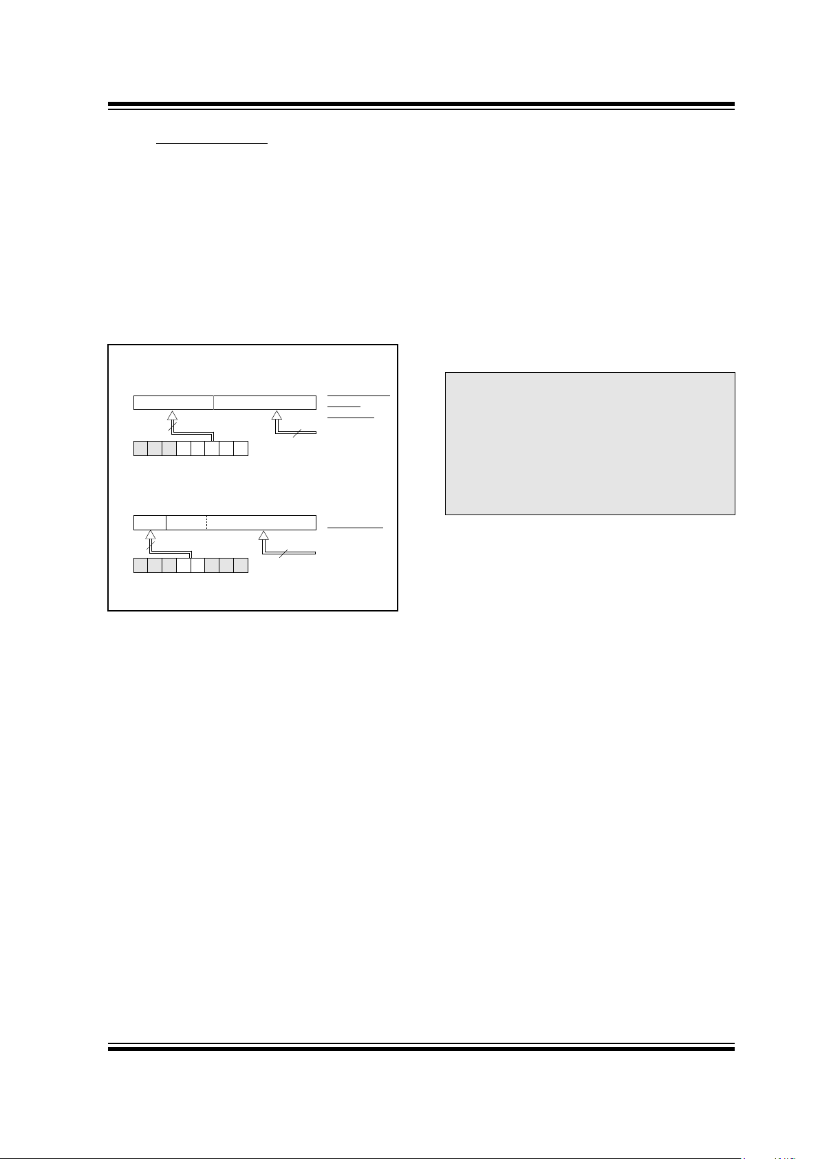
4.3 PCL and PCLATH
The program counter (PC) is 13-bits wide. The low byte
comes from the PCL register, which is a readable and
writable register. The high bits (PC<12:8>) are not directly
readable or writable and come from PCLATH. On any
reset, the PC is cleared. Figure 4-10 shows the two
situations for the loading of the PC. The upper example in
the figure shows how the PC is loaded on a write to PCL
(PCLATH<4:0> → PCH). The lo wer example in the figure
shows how the PC is loaded during a CALL or GOTO
instruction (PCLATH<4:3> → PCH).
FIGURE 4-10: LOADING OF PC IN
DIFFERENT SITUATIONS
4.3.1 COMPUTED GOTO
A computed GOTO is accomplished by adding an
offset to the program counter (ADDWF PCL). When doing
a table read using a computed GOTO method, care
should be exercised if the tab le location crosses a PCL
memory boundary (each 256 byte block). Refer to the
application note
“Implementing a Table Read"
(AN556).
PC
12 8 7 0
5
PCLA TH<4:0>
PCLA TH
Instr
uction with
ALU result
GOTO, CALL
Opcode <10:0>
8
PC
12 11 10 0
11
PCLATH<4:3>
PCH PCL
8 7
2
PCLATH
PCH PCL
PCL as
Destination
4.3.2 STACK
The PIC16C55X(A) family has an 8 level deep x 13-bit
wide hardware stack (Figure 4-1, Figure 4-2 and
Figure 4-3). The stack space is not part of either pro-
gram or data space and the stack pointer is not read-
able or writable. The PC is PUSHed onto the stack
when a CALL instruction is executed or an interrupt
causes a branch. The stack is POPed in the event of a
RETURN, RETLW or a RETFIE instruction execution.
PCLATH is not affected by a PUSH or POP operation.
The stack operates as a circular buff er . This means that
after the stack has been PUSHed eight times, the ninth
push overwrites the value that was stored from the first
push. The tenth push overwrites the second push (and
so on).
Note 1: There are no STATUS bits to indicate
stack overflow or stack underflow
conditions.
Note 2: There are no instructions mnemonics
called PUSH or POP. These are actions
that occur from the execution of the
CALL, RETURN, RETLW and RETFIE
instructions, or vectoring to an interrupt
address.
PIC16C55X(A)
DS40143B-page 22 Preliminary 1997 Microchip Technology Inc.
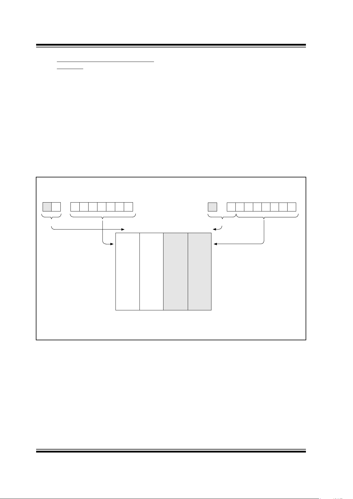
4.4 Indirect Addressing, INDF and FSR
Registers
The INDF register is not a physical register . Addressing
the INDF register will cause indirect addressing.
Indirect addressing is possible by using the INDF reg-
ister. Any instruction using the INDF register actually
accesses data pointed to by the file select register
(FSR). Reading INDF itself indirectly will produce 00h.
Writing to the INDF register indirectly results in a
no-operation (although status bits may be affected). An
effective 9-bit address is obtained by concatenating the
8-bit FSR register and the IRP bit (STATUS<7>), as
shown in Figure 4-11. However, IRP is not used in the
PIC16C55X(A).
A simple program to clear RAM locations 20h-2Fh
using indirect addressing is shown in Example 4-1.
EXAMPLE 4-1: INDIRECT ADDRESSING
movlw 0x20 ;initialize pointer
movwf FSR ;to RAM
N
EXT clrf INDF ;clear INDF register
incf FSR ;inc pointer
btfss FSR,4 ;all done?
goto NEXT ;no clear next
;yes continue
CONTINUE:
FIGURE 4-11: DIRECT/INDIRECT ADDRESSING PIC16C55X(A)
For memory map detail see Figure 4-4 and Figure 4-5.
Note 1: The RP1 and IRP bits are reserved, always maintain these bits clear.
Data
Memory
Indirect AddressingDirect Addressing
bank select location select
(1)
RP1 RP0 6
0
from opcode
IRP
(1)
FSR register
7
0
bank select
location select
00 01 10 11
00h
7Fh
00h
7Fh
Bank 0 Bank 1 Bank 2 Bank 3
not used
1997 Microchip Technology Inc. Preliminary DS40143B-page 23
PIC16C55X(A)
5.0 I/O PORTS
The PIC16C55X(A) ha ve two ports, PORT A and POR TB.
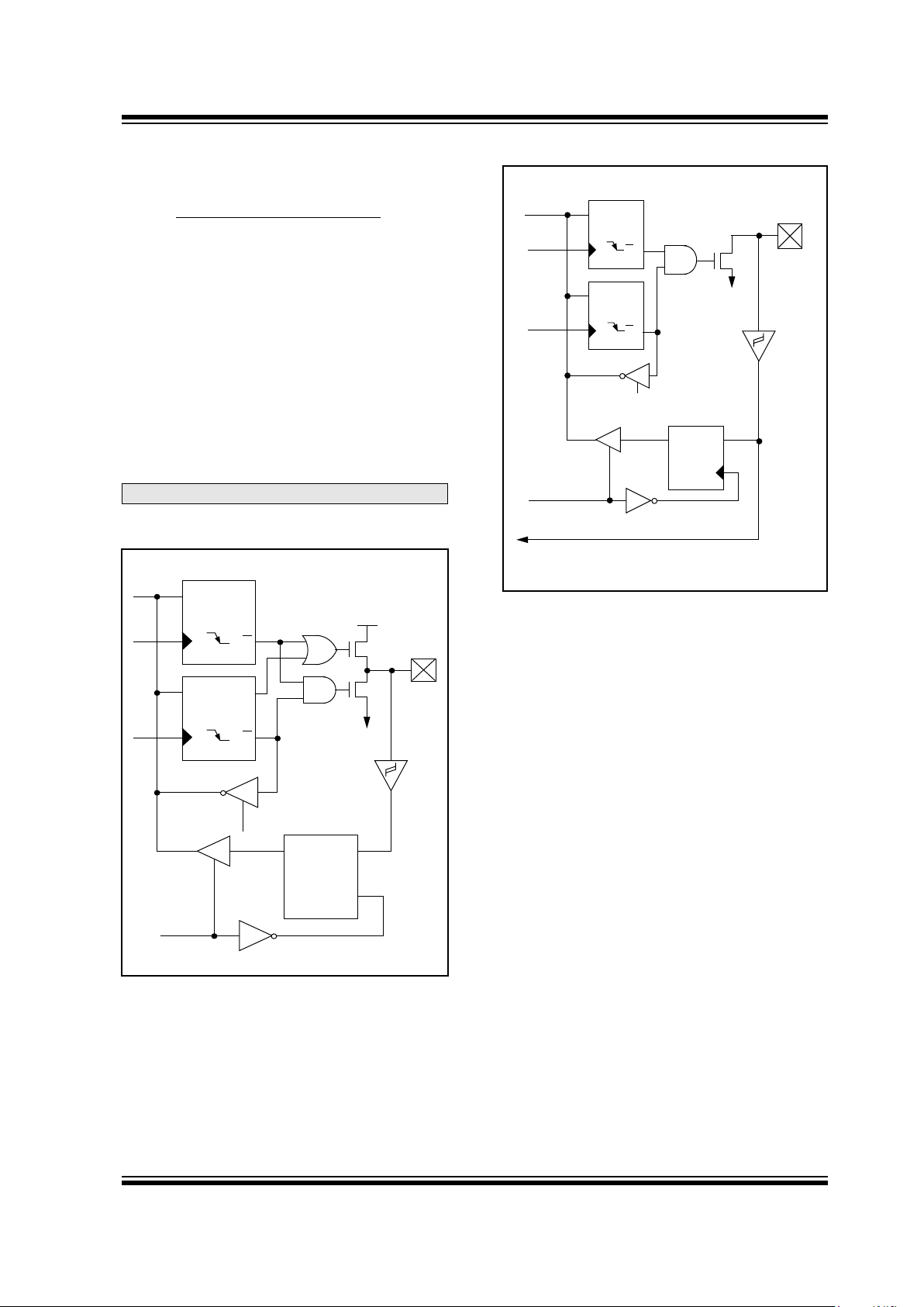
5.1 PORT A and TRISA Registers
PORTA is a 5-bit wide latch. RA4 is a Schmitt Trigger input
and an open drain output. Port RA4 is multiple xed with the
T0CKI clock input. All other RA port pins have Schmitt
Trigger input levels and full CMOS output driv ers . All pins
have data direction bits (TRIS registers) which can config-
ure these pins as input or output.
A '1' in the TRISA register puts the corresponding output
driver in a hi- impedance mode. A '0' in the TRISA register
puts the contents of the output latch on the selected pin(s).
Reading the PORTA register reads the status of the pins,
whereas writing to it will write to the port latch. All write
operations are read-modify-write operations. So a write
to a port implies that the port pins are first read, then this
value is modified and written to the port data latch.
FIGURE 5-1: BLOCK DIAGRAM OF
PORT PINS RA<3:0>
Note: On reset, the TRISA register is set to all inputs.
Data
bus
Q
D
Q
CK
QD
Q
CK
Q D
EN
P
N
WR
PortA
WR
TRISA
Data Latch
TRIS Latch
RD TRISA
RD PORTA
Schmitt
input
buffer
V
SS
VDD
I/O pin
Trigger
FIGURE 5-2: BLOCK DIAGRAM OF RA4 PIN
Data
bus
WR
PORTA
WR
TRISA
RD PORTA
Data Latch
TRISA Latch
RD TRISA
Schmitt
Trigger
input
buffer
N
V
SS
I/O pin
(1)
TMR0 clock input
Note 1: I/O pin has protection diodes to V
SS only.
QD
Q
CK
QD
Q
CK
EN
Q D
EN
PIC16C55X(A)
DS40143B-page 24 Preliminary 1997 Microchip Technology Inc.
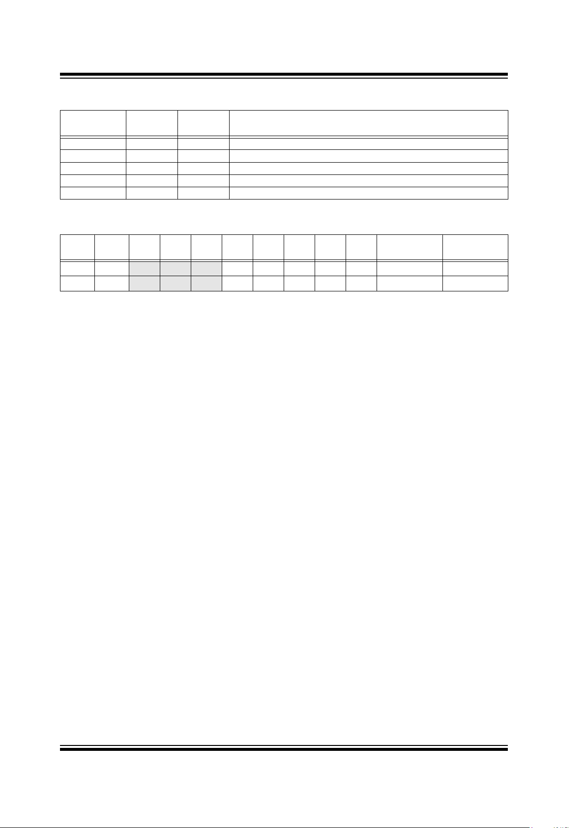
TABLE 5-1: PORTA FUNCTIONS
TABLE 5-2: SUMMARY OF REGISTERS ASSOCIATED WITH PORTA
Name Bit #
Buffer
Type
Function
RA0 bit0 ST Input/output
RA1 bit1 ST Input/output
RA2 bit2 ST Input/output
RA3 bit3 ST Input/output
RA4/T0CKI bit4 ST Input/output or external clock input for TMR0. Output is open drain type.
Legend: ST = Schmitt Trigger input
Address Name Bit 7 Bit 6 Bit 5 Bit 4 Bit 3 Bit 2 Bit 1 Bit 0
Value on
POR
Value on
All Other Resets
05h PORTA — — — RA4 RA3 RA2 RA1 RA0
---x xxxx ---u uuuu
85h TRISA — — — TRISA4 TRISA3 TRISA2 TRISA1 TRISA0
---1 1111 ---1 1111
Legend: — = Unimplemented locations, read as ‘0’
Note: Note: Shaded bits are not used by PORTA.
1997 Microchip Technology Inc. Preliminary DS40143B-page 25
PIC16C55X(A)
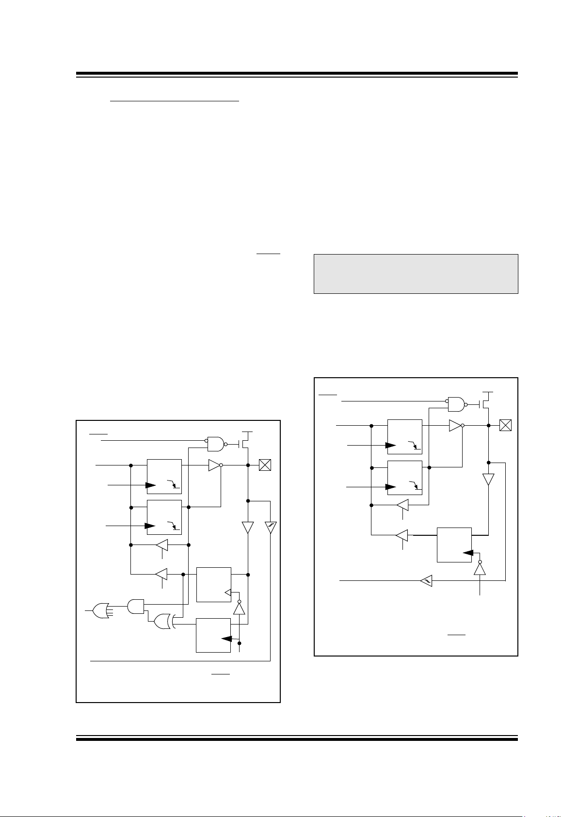
5.2 PORTB and TRISB Registers
PORTB is an 8-bit wide bi-directional port. The
corresponding data direction register is TRISB. A '1' in
the TRISB register puts the corresponding output driver
in a high impedance mode. A '0' in the TRISB register
puts the contents of the output latch on the selected
pin(s).
Reading PORTB register reads the status of the pins,
whereas writing to it will write to the port latch. All write
operations are read-modify-write operations. So a write
to a port implies that the por t pins are first read, then
this value is modified and written to the port data latch.
Each of the PORTB pins has a weak internal pull-up
(≈200 µA typical). A single control bit can turn on all the
pull-ups. This is done by clearing the RBPU
(OPTION<7>) bit. The weak pull-up is automatically
turned off when the port pin is configured as an output.
The pull-ups are disabled on Power-on Reset.
Four of PORTB’s pins, RB7:RB4, have an interrupt on
change feature. Only pins configured as inputs can
cause this interrupt to occur (i.e., any RB7:RB4 pin
configured as an output is excluded from the interrupt
on change comparison). The input pins (of RB7:RB4)
are compared with the old value latched on the last
read of PORTB. The “mismatch” outputs of RB7:RB4
are OR’ed together to generate the RBIF interrupt (flag
latched in INTCON<0>).
FIGURE 5-3: BLOCK DIAGRAM OF
RB7:RB4 PINS
Data Latch
From other
RBPU
(2)
P
V
DD
I/O
QD
CK
QD
CK
Q D
EN
Q D
EN
Data bus
WR PortB
WR TRISB
Set RBIF
TRIS Latch
RD TRISB
RD PortB
RB7:RB4 pins
weak
pull-up
RD Port
Latch
TTL
Input
Buffer
pin
(1)
Note 1: I/O pins have diode protection to VDD and VSS.
Note 2: TRISB = 1 enables weak pull-up if RBPU
= '0'
(OPTION<7>).
ST
Buffer
RB7:RB6 in serial programming mode
This interrupt can wake the device from SLEEP. The
user, in the interrupt service routine, can clear the
interrupt in the following manner:
a) Any read or write of PORTB. This will end the
mismatch condition.
b) Clear flag bit RBIF.
A mismatch condition will continue to set flag bit RBIF.
Reading PORTB will end the mismatch condition, and
allow flag bit RBIF to be cleared.
This interrupt on mismatch feature, together with
software configurable pull-ups on these four pins allow
easy interface to a key pad and make it possible for
wake-up on key-depression. (See AN552 in the
Microchip
Embedded Control Handbook
.)
The interrupt on change feature is recommended for
wake-up on key depression operation and operations
where PORTB is only used for the interrupt on change
feature. Polling of PORTB is not recommended while
using the interrupt on change feature.
FIGURE 5-4: BLOCK DIAGRAM OF
RB3:RB0 PINS
Note: If a change on the I/O pin should occur when the
read operation is being executed (start of the Q2
cycle), then the RBIF interrupt flag may not
get set.
Data Latch
RBPU
(2)
P
V
DD
QD
CK
QD
CK
Q D
EN
Data bus
WR PortB
WR TRISB
RD TRISB
RD PortB
weak
pull-up
RD Port
RB0/INT
I/O
pin
(1)
TTL
Input
Buffer
Note 1: I/O pins have diode protection to VDD and VSS.
Note 2: TRISB = 1 enables weak pull-up if RBPU
= '0'
(OPTION<7>).
ST
Buffer
PIC16C55X(A)
DS40143B-page 26 Preliminary 1997 Microchip Technology Inc.
TABLE 5-3: PORTB FUNCTIONS
TABLE 5-4: SUMMARY OF REGISTERS ASSOCIATED WITH PORTB
Name Bit # Buffer Type Function
RB0/INT bit0
TTL/ST
(1)
Input/output or external interrupt input. Internal software programmable
weak pull-up.
RB1 bit1 TTL Input/output pin. Internal software programmable weak pull-up.
RB2 bit2 TTL Input/output pin. Internal software programmable weak pull-up.
RB3 bit3 TTL Input/output pin. Internal software programmable weak pull-up.
RB4 bit4 TTL Input/output pin (with interrupt on change). Internal software
programmable weak pull-up.
RB5 bit5 TTL Input/output pin (with interrupt on change). Internal software
programmable weak pull-up.
RB6 bit6
TTL/ST
(2)
Input/output pin (with interrupt on change). Internal software
programmable weak pull-up. Serial programming clock pin.
RB7 bit7
TTL/ST
(2)
Input/output pin (with interrupt on change). Internal software
programmable weak pull-up. Serial programming data pin.
Legend: ST = Schmitt Trigger, TTL = TTL input
Note 1: This buffer is a Schmitt Trigger input when configured as the external interrupt.
Note 2: This buffer is a Schmitt Trigger input when used in serial programming mode.
Address Name Bit 7 Bit 6 Bit 5 Bit 4 Bit 3 Bit 2 Bit 1 Bit 0
Value on
POR
Value on
All Other Rests
06h PORTB RB7 RB6 RB5 RB4 RB3 RB2 RB1 RB0
uuuu uuuu xxxx xxxx
86h TRISB TRISB7 TRISB6 TRISB5 TRISB4 TRISB3 TRISB2 TRISB1 TRISB0
1111 1111 1111 1111
81h OPTION RBPU INTEDG T0CS T0SE PSA PS2 PS1 PS0
1111 1111 1111 1111
Note: Shaded bits are not used by PORTB.
1997 Microchip Technology Inc. Preliminary DS40143B-page 27
PIC16C55X(A)
5.3 I/O Programming Considerations
5.3.1 BI-DIRECTIONAL I/O PORTS
Any instruction which writes, operates internally as a
read followed by a write operation. The BCF and BSF
instructions, for example, read the register into the
CPU, ex ecute the bit operation and write the result back
to the register. Caution must be used when these
instructions are applied to a port with both inputs and
outputs defined. For example, a BSF operation on bit5
of PORTB will cause all eight bits of PORTB to be read
into the CPU. Then the BSF operation takes place on
bit5 and PORTB is written to the output latches. If
another bit of PORTB is used as a bidirectional I/O pin
(e.g., bit0) and it is defined as an input at this time, the
input signal present on the pin itself would be read into
the CPU and re-written to the data latch of this
particular pin, overwriting the previous content. As long
as the pin stays in the input mode, no problem occurs.
However, if bit0 is switched into output mode later on,
the content of the data latch may now be unknown.
Reading the port register, reads the values of the port
pins. Writing to the port register writes the value to the
port latch. When using read modify write instructions
(ex. BCF, BSF , etc.) on a port, the value of the port pins
is read, the desired operation is done to this value, and
this value is then written to the port latch.
Example 5-1 shows the effect of two sequential
read-modify-write instructions (ex., BCF, BSF, etc.) on
an I/O port.
A pin actively outputting a Low or High should not be
driven from external devices at the same time in order
to change the level on this pin (“wired-or”, “wired-and”).
The resulting high output currents may damage
the chip.
EXAMPLE 5-1: READ-MODIFY-WRITE
INSTRUCTIONS ON AN
I/O PORT
5.3.2 SUCCESSIVE OPERATIONS ON I/O PORTS
The actual write to an I/O port happens at the end of an
instruction cycle, whereas for reading, the data must be
valid at the beginning of the instruction cycle
(Figure 5-5). Therefore, care must be exercised if a
write followed by a read operation is carried out on the
same I/O port. The sequence of instructions should be
such to allow the pin voltage to stabilize (load
dependent) before the next instruction which causes
that file to be read into the CPU is executed. Otherwise ,
the previous state of that pin may be read into the CPU
rather than the new state. When in doubt, it is better to
separate these instructions with an NOP or another
instruction not accessing this I/O port.
;
;
Initial PORT settings: PORTB<7:4> Inputs
; PORTB<3:0> Outputs
;
;
PORTB<7:6> have external pull-up and are not
connected to other circuitry
;
; PORT latch PORT pins
; ---------- ----------
BCF PORTB, 7 ; 01pp pppp 11pp pppp
BCF PORTB, 6 ; 10pp pppp 11pp pppp
BSF STATUS,RP0 ;
BCF TRISB, 7 ; 10pp pppp 11pp pppp
BCF TRISB, 6 ; 10pp pppp 10pp pppp
;
; Note that the user may have expected the pin
; values to be 00pp pppp. The 2nd BCF caused
; RB7 to be latched as the pin value (High).
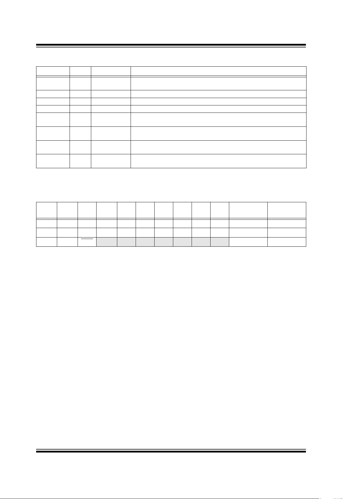
FIGURE 5-5: SUCCESSIVE I/O OPERATION
Note:
This example shows write to PORTB
followed by a read from PORTB.
Note that:
data setup time = (0.25 T
CY - TPD)
where TCY = instruction cycle and
TPD = propagation delay of Q1 cycle
to output valid.
Therefore, at higher clock frequencies,
a write followed by a read may be
problematic.
Q1 Q2 Q3 Q4 Q1 Q2 Q3 Q4 Q1 Q2 Q3 Q4 Q1 Q2 Q3 Q4
RB <7:0>
Port pin
sampled here
PC
PC + 1 PC + 2 PC + 3
NOPNOPMOVF PORTB, W
Read PORTB
MOVWF PORTB
Write to
PORTB
PC
Instruction
fetched
TPD
Execute
MOVWF
PORTB
Execute
MOVF
PORTB, W
Execute
NOP
RB7:RB0

PIC16C55X(A)
DS40143B-page 28 Preliminary 1997 Microchip Technology Inc.
NOTES:
1997 Microchip Technology Inc. Preliminary DS40143B-page 29
PIC16C55X(A)
6.0 TIMER0 MODULE
The Timer0 module timer/counter has the following
features:
• 8-bit timer/counter
• Readable and writable
• 8-bit software programmable prescaler
• Internal or external clock select
• Interrupt on overflow from FFh to 00h
• Edge select for external clock
Figure 6-1 is a simplified block diagram of the Timer0
module.
Timer mode is selected by clearing the T0CS bit
(OPTION<5>). In timer mode, the TMR0 will increment
every instruction cycle (without prescaler). If Timer0 is
written, the increment is inhibited for the following two
cycles (Figure 6-2 and Figure 6-3). The user can work
around this by writing an adjusted value to TMR0.
Counter mode is selected by setting the T0CS bit. In
this mode Timer0 will increment either on every rising
or falling edge of pin RA4/T0CKI. The incrementing
edge is determined by the source edge (T0SE) control
bit (OPTION<4>). Clearing the T0SE bit selects the
rising edge. Restrictions on the e xternal clock input are
discussed in detail in Section 6.2.
The prescaler is shared between the Timer0 module
and the WatchdogTimer. The prescaler assignment is
controlled in software by the control bit PSA
(OPTION<3>). Clearing the PSA bit will assign the
prescaler to Timer0. The prescaler is not readable or
writable. When the prescaler is assigned to the Timer0
module, prescale value of 1:2, 1:4, ..., 1:256 are
selectable. Section 6.3 details the operation of the
prescaler.
6.1 TIMER0 Interrupt
Timer0 interrupt is generated when the TMR0 register
timer/counter overflows from FFh to 00h. This overflow
sets the T0IF bit. The interrupt can be masked by
clearing the T0IE bit (INTCON<5>). The T0IF bit
(INTCON<2>) must be cleared in software by the
Timer0 module interrupt service routine before
re-enabling this interrupt. The Timer0 interrupt cannot
wake the processor from SLEEP since the timer is shut
off during SLEEP. See Figure 6-4 for Timer0 interrupt
timing.
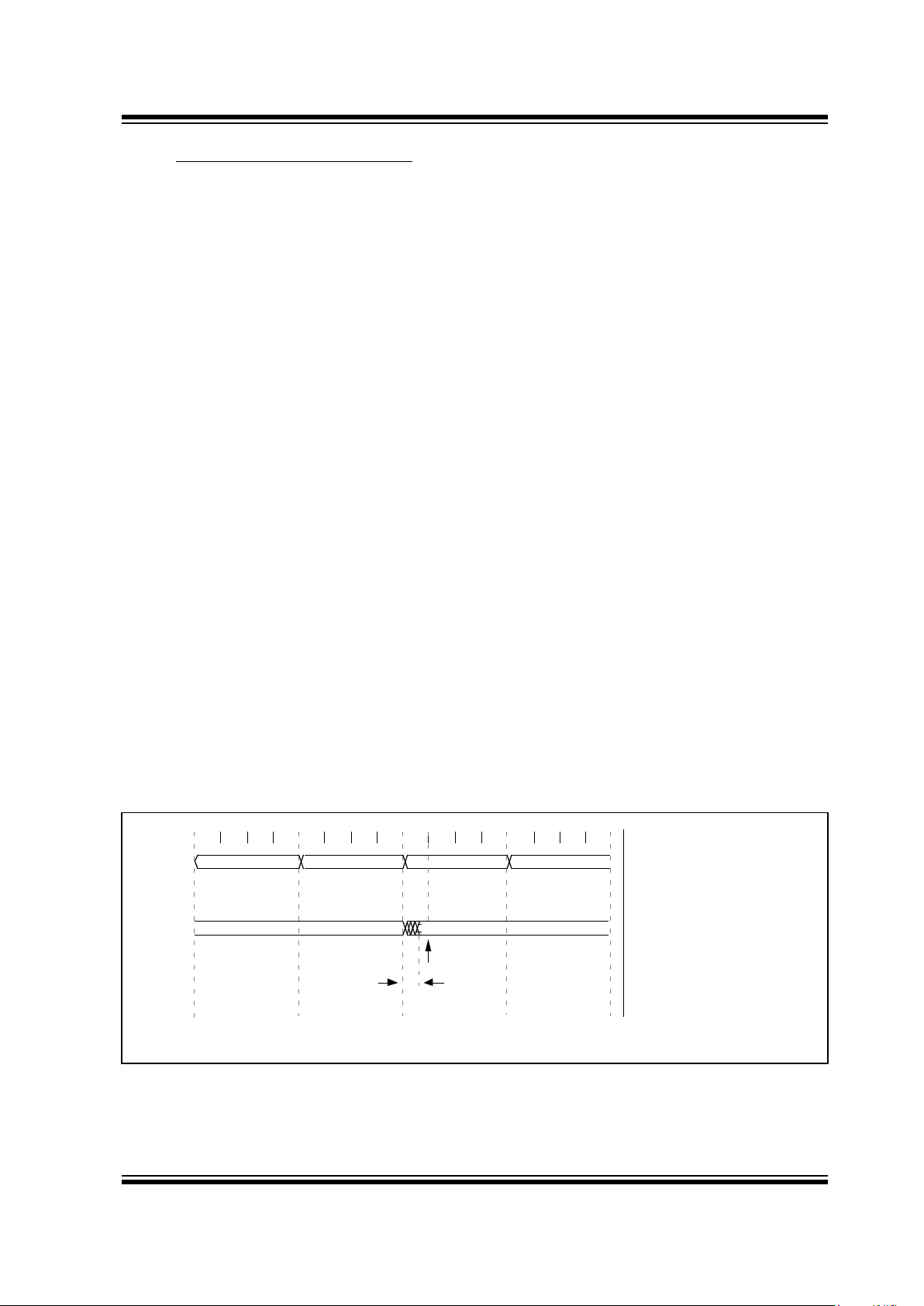
FIGURE 6-1: TIMER0 BLOCK DIAGRAM
FIGURE 6-2: TIMER0 (TMR0) TIMING: INTERNAL CLOCK/NO PRESCALER
Note 1: Bits, T0SE, T0CS, PS2, PS1, PS0 and PSA are located in the OPTION register.
2: The prescaler is shared with Watchdog Timer (Figure 6-6)
RA4/T0CKI
T0SE
0
1
1
0
pin
T0CS
FOSC/4
Programmable
Prescaler
Sync with
Internal
clocks
TMR0
PSout
(2 cycle delay)
PSout
Data bus
8
Set Flag bit T0IF
on Overflow
PSA
PS2:PS0
PC-1
Q1 Q2 Q3 Q4
Q1 Q2 Q3 Q4 Q1 Q2 Q3 Q4 Q1 Q2 Q3 Q4 Q1 Q2 Q3 Q4 Q1 Q2 Q3 Q4 Q1 Q2 Q3 Q4 Q1 Q2 Q3 Q4
PC
(Program
Counter)
Instruction
Fetch
TMR0
PC PC+1 PC+2 PC+3 PC+4 PC+5 PC+6
T0
T0+1 T0+2 NT0 NT0 NT0 NT0+1 NT0+2
T0
MOVWF TMR0
MOVF TMR0,W MOVF TMR0,W MOVF TMR0,W MOVF TMR0,W MOVF TMR0,W
Write TMR0
executed
Read TMR0
reads NT0
Read TMR0
reads NT0
Read TMR0
reads NT0
Read TMR0
reads NT0 + 1
Read TMR0
reads NT0 + 2
Instruction
Executed
 Loading...