


Microchip Technology Inc 37LV36-TI-P, 37LV36-TI-L, 37LV36-T-P, 37LV36-T-L, 37LV36-I-SN Datasheet
...
37LV36/65/128
36K, 64K, and 128K Serial EPROM Family
FEATURES
•Operationally equivalent to Xilinx XC1700 family
•Wide voltage range 3.0 V to 6.0 V
•Maximum read current 10 mA at 5.0 V
•Standby current 100 A typical
•Industry standard Synchronous Serial Interface/ 1 bit per rising edge of clock
•Full Static Operation
•Sequential Read/Program
•Cascadable Output Enable
•10 MHz Maximum Clock Rate @ 5.0 Vdc
•Programmable Polarity on Hardware Reset
•Programming with industry standard EPROM programmers
•Electrostatic discharge protection > 4,000 volts
•8-pin PDIP/SOIC and 20-pin PLCC packages
•Data Retention > 200 years
•Temperature ranges:
- Commercial: 0°C to +70°C - Industrial: -40°C to +85°C
DESCRIPTION
The Microchip Technology Inc. 37LV36/65/128 is a family of Serial OTP EPROM devices organized internally in a x32 configuration. The family also features a cascadable option for increased memory storage where needed. The 37LV36/65/128 is suitable for many applications in which look-up table information storage is desirable and provides full static operation in the 3.0V to 6.0V VCC range. The devices also support the industry standard serial interface to the popular RAM-based Field Programmable Gate Arrays (FPGA). Advanced CMOS technology makes this an ideal bootstrap solution for today's high speed SRAM-based FPGAs. The 37LV36/65/128 family is available in the standard 8-pin plastic DIP, 8-pin SOIC and 20-pin PLCC packages.
Device |
Bits |
Programming Word |
|
|
|
|
|
|
37LV36 |
36,288 |
1134 x 32 |
|
|
|
37LV65 |
65,536 |
2048 x 32 |
|
|
|
37LV128 |
131,072 |
4096 x 32 |
|
|
|
Xilinx is a registered trademark of Xilinx Corporation.
1996 Microchip Technology Inc.
PACKAGE TYPES
PDIP
DATA 1 |
8 |
VCC |
RESET/OE |
3 |
37LV128 |
37LV65 |
37LV36 |
6 |
CEO |
||
CLK |
2 |
|
|
|
|
|
7 |
VPP |
CE |
4 |
|
|
|
|
|
5 |
VSS |
SOIC |
|
|
|
|
|
|
|
|
DATA |
1 |
37LV128 |
37LV65 |
|
37LV36 |
|
8 |
VCC |
RESET/OE |
3 |
|
|
6 |
CEO |
|||
CLK |
2 |
|
|
|
|
|
7 |
VPP |
CE |
4 |
|
|
|
|
|
5 |
VSS |
PLCC |
|
|
|
|
|
|
|
|
|
DATA VCC |
|
|
|
||||
|
3 |
2 |
1 |
20 |
19 |
|
|
|
CLK |
4 |
37LV128 |
37LV65 |
|
37LV36 |
|
18 |
|
RESET/OE |
5 |
|
|
17 |
VPP |
|||
|
|
|
|
|
||||
6 |
|
|
|
|
|
16 |
|
|
|
7 |
|
|
|
|
|
15 |
|
|
|
|
|
|
|
|
|
|
CE 8 |
|
|
|
|
|
14 |
CEO |
|
|
9 |
10 |
11 |
12 |
13 |
|
|
|
Vss
BLOCK DIAGRAM
CE
 CEO
CEO
RESET/OE
|
|
|
|
|
|
OE |
|
|
|
|
|
|
|
||
ADDRESS |
EPROM |
|
|
|
|||
|
|
|
|
DATA |
|||
Counter |
ARRAY |
|
|
|
|
||
|
|
|
|
|
|||
|
|
|
|
|
|
|
|
CLK
DS21109E-page 1

37LV36/65/128
1.0ELECTRICAL CHARACTERISTICS
1.1Maximum Ratings*
VCC and input voltages w.r.t. VSS .......... |
-0.6V to +0.6V |
|
VPP voltage w.r.t. VSS during |
|
|
programming ...................................... |
-0.6V to +14.0V |
|
Output voltage w.r.t. VSS ............... |
-0.6V to VCC +0.6V |
|
Storage temperature .......................... |
-65˚C to +150˚C |
|
Ambient temp. with power applied ..... |
-65˚C to +125˚C |
|
Soldering temperature of leads (10 sec.) ......... |
+300°C |
|
ESD protection on all pins ..................................... |
|
≥ 4 kV |
*Notice: Stresses above those listed under “Maximum Ratings” may cause permanent damage to the device. This is a stress rating only and functional operation of the device at those or any other conditions above those indicated in the operation listings of this specification is not implied. Exposure to maximum rating conditions for extended periods may affect device reliability.
TABLE 1-1: |
PIN FUNCTION TABLE |
|
|
||||||
|
|
|
|
||||||
Name |
Function |
8 |
20 |
||||||
|
|
|
|
||||||
|
|
|
|
||||||
DATA |
Data I/O |
1 |
2 |
||||||
|
CLK |
Clock Input |
2 |
4 |
|||||
|
|
|
|
|
|
|
Reset Input and Output |
3 |
6 |
RESET/OE |
|
||||||||
|
|
|
|
|
|
|
Enable |
|
|
|
|
|
|
|
Chip Enable Input |
4 |
8 |
||
CE |
|||||||||
|
VSS |
Ground |
5 |
10 |
|||||
|
|
|
Chip Enable Output |
6 |
14 |
||||
CEO |
|||||||||
|
VPP |
Programming Voltage Supply |
7 |
17 |
|||||
|
VCC |
+3.0V to 6.0V Power Supply |
8 |
20 |
|||||
Not Labeled |
Not utilized, not connected |
|
|
||||||
|
|
|
|
|
|
|
|
|
|
TABLE 1-2: |
READ OPERATION DC CHARACTERISTICS |
|
|
||||||||
|
|
|
|
|
|
|
|
|
|
|
|
|
|
|
|
|
|
|
|
VCC = +3.0 to 6.0V |
|||
|
|
|
|
|
|
|
|
Commercial (C): Tamb = 0˚C to +70˚C |
|||
|
|
|
|
|
|
|
|
Industrial (I): |
Tamb = -40˚C to +85˚C |
||
|
|
|
|
|
|
|
|
|
|||
|
|
Parameter |
Symbol |
Min. |
Max. |
|
Units |
Conditions |
|||
|
|
|
|
|
|
|
|
|
|
|
|
|
|
|
|
|
|
|
|
|
|
|
|
DATA, |
|
|
|
and Reset pins: |
|
|
|
|
|
|
|
CE, |
CEO |
|
|
|
|
|
|
||||
High level input voltage |
VIH |
2.0 |
VCC |
|
V |
|
|||||
Low level input voltage |
VIL |
-0.3 |
0.8 |
|
V |
IOH = -4 mA VCC ≥ 4.5V |
|||||
High level output voltage |
VOH1 |
3.86 |
|
|
V |
||||||
|
|
|
|
|
|
VOH2 |
2.4 |
|
|
|
IOH = -4 mA VCC ≥ 3.0V |
Low level output voltage |
VOL |
— |
.32 |
|
V |
IOL = 4.0 mA |
|||||
|
|
|
|
|
|
|
|
||||
Input Leakage |
|
ILI |
-10 |
10 |
|
A |
VIN = .1V to VCC |
||||
|
|
|
|
|
|
|
|
||||
Output Leakage |
|
ILO |
-10 |
10 |
|
A |
VOUT = .1V to VCC |
||||
|
|
|
|
|
|
|
|||||
Input Capacitance |
CINT |
— |
10 |
|
pF |
Tamb = 25 °C; FCLK = 1 MHz (Note 1) |
|||||
(all inputs/outputs) |
|
|
|
|
|
|
|||||
|
|
|
|
|
|
|
|||||
Operating Current |
ICC Read |
— |
10 |
|
mA |
VCC = 6.0V, CLK = 10 MHz |
|||||
|
|
|
|
|
|
|
— |
2 |
|
mA |
VCC = 3.6V, CLK = 2.5 MHz |
|
|
|
|
|
|
|
|
|
|
|
Outputs open |
|
|
|
|
|
|
|
|
||||
Standby Current |
|
ICCS |
— |
100 |
|
A |
VCC = 6.0V, CE = 5.8V |
||||
|
|
|
|
|
|
|
|
50 |
|
A |
VCC = 3.6V, CE = 3.4V |
|
|
|
|
|
|
|
|
|
|
|
|
Note 1: This parameter is initially characterized and not 100% tested.
DS21109E-page 2 |
1996 Microchip Technology Inc. |

37LV36/65/128
2.0DATA
2.1Data I/O
Three-state DATA output for reading and input during programming.
3.0CLK
3.1Clock Input
Used to increment the internal address and bit counters for reading and programming.
4.0RESET/OE
4.1Reset Input and Output Enable
A LOW level on both the CE and RESET/OE inputs enables the data output driver. A HIGH level on RESET/OE resets both the address and bit counters. In the 37LVXXX, the logic polarity of this input is programmable as either RESET/OE or OE/RESET. This document describes the pin as RESET/OE although the opposite polarity is also possible. This option is defined and set at device program time.
5.0CE
5.1Chip Enable Input
CE is used for device selection. A LOW level on both CE and OE enables the data output driver. A HIGH level on CE disables both the address and bit counters and forces the device into a low power mode.
6.0CEO
6.1Chip Enable Output
This signal is asserted LOW on the clock cycle following the last bit read from the memory. It will stay LOW as long as CE and OE are both LOW. It will then follow CE until OE goes HIGH. Thereafter, CEO will stay HIGH until the entire EPROM is read again. This pin also used to sense the status of RESET polarity when Programming Mode is entered.
7.0VPP
7.1Programming Voltage Supply
Used to enter programming mode (+13 volts) and to program the memory (+13 volts). Must be connected directly to Vcc for normal Read operation. No overshoot above +14 volts is permitted.
8.0CASCADING SERIAL EPROMS
Cascading Serial EPROMs provide additional memory for multiple FPGAs configured as a daisy-chain, or for future applications requiring larger configuration memories.
When the last bit from the first Serial EPROM is read, the next clock signal to the Serial EPROM asserts its CEO output LOW and disables its DATA line. The sec-
ond Serial EPROM recognizes the LOW level on its CE input and enables its DATA output.
When configuration is complete, the address counters of all cascaded Serial EPROMs are reset if RESET
goes LOW forcing the RESET/OE on each Serial EPROM to go HIGH. If the address counters are not to
be reset upon completion, then the RESET/OE inputs can be tied to ground.
Additional logic may be required if cascaded memories are so large that the rippled chip enable is not fast enough to activate successive Serial EPROMs.
9.0STANDBY MODE
The 37LVXXX enters a low-power Standby Mode whenever CE is HIGH. In Standby Mode, the Serial EPROM consumes less than 100 A of current. The output will remain in a high-impedance state regardless of the state of the OE input.
10.0PROGRAMMING MODE
Programming Mode is entered by holding VPP HIGH (+13 volts) for two clock edges and then holding VPP = VDD for one clock edge. Programming mode is exited
by driving a LOW on both CE and OE and then removing power from the device. Figures 4 through 7 show the programming algorithm.
11.037LVXXX RESET POLARITY
The 37LVXXX lets the user choose the reset polarity as either RESET/OE or OE/RESET. Any third-party commercial programmer should prompt the user for the desired reset polarity.
The programming of the overflow word should be handled transparently by the EPROM programmer; it is mentioned here as supplemental information only.
The polarity is programmed into the first overflow word location, maximum address+1. 00000000 in these locations makes the reset active LOW, FFFFFFFF in these locations makes the reset active HIGH. The default condition is RESET active HIGH.
1996 Microchip Technology Inc. |
DS21109E-page 3 |
37LV36/65/128
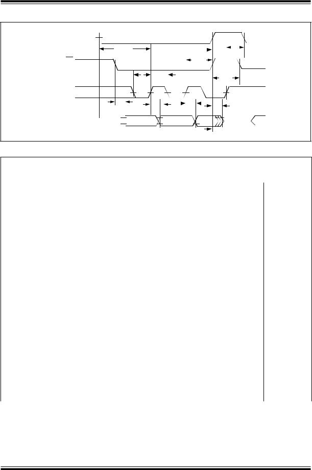
FIGURE 11-1: READ CHARACTERISTICS TIMING
CE 
TSCE |
|
|
TSCE |
THCE |
TSCED |
|
|
||
|
|
|
||
RESET/OE |
|
THCED |
|
|
|
TLC |
THC |
THOE |
|
|
|
|||
CLK |
|
|
|
|
TOE |
TCAC |
TOH |
|
TDF |
|
|
|||
 TCE
TCE 
DATA
 TOH
TOH
TABLE 11-1: READ CHARACTERISTICS
AC Testing Waveform: VIL = 0.2V; VIH = 3.0V
AC Test Load: 50 pF
VOL = VOL_MAX; VOH = VOH_MIN
|
|
|
|
|
|
|
|
|
|
|
|
Limits 3.0V ≤ |
Limits 4.5V ≤ |
|
|
|
||
Symbol |
|
|
|
|
|
|
Parameter |
Vcc ≤ 6.0V |
Vcc ≤ 6.0V |
Units |
|
Conditions |
||||||
|
|
|
|
|
|
|
|
|
|
|
||||||||
|
|
|
|
|
|
|
|
|
|
|
|
Min. |
Max. |
Min. |
Max. |
|
|
|
|
|
|
|
|
|
|
|
|
|
|
|
|
||||||
|
|
|
|
|
|
|
|
|
|
|
|
|
||||||
TOE |
|
|
|
|
to Data Delay |
— |
45 |
— |
45 |
ns |
|
|
||||||
OE |
|
|
||||||||||||||||
|
|
|
|
|
|
|
|
|
|
|
|
|||||||
TCE |
|
|
|
to Data Delay |
— |
60 |
— |
50 |
ns |
|
|
|||||||
CE |
|
|
||||||||||||||||
|
|
|
|
|
|
|
|
|
|
|||||||||
TCAC |
|
CLK to Data Delay |
— |
200 |
— |
60 |
ns |
|
|
|||||||||
|
|
|
|
|
|
|
|
|
|
|
|
|
|
|||||
TOH |
|
Data Hold from |
|
|
|
or CLK |
0 |
— |
0 |
— |
ns |
|
|
|||||
CE, |
OE |
|
|
|||||||||||||||
|
|
|
|
|
|
|
|
|
|
|
|
|
||||||
TDF |
|
|
or |
|
to Data Float Delay |
— |
50 |
— |
50 |
ns |
|
Notes 1, 2 |
||||||
CE |
OE |
|||||||||||||||||
|
|
|
|
|
|
|
|
|
|
|||||||||
TLC |
|
CLK Low Time |
100 |
— |
25 |
— |
ns |
|
|
|||||||||
|
|
|
|
|
|
|
|
|
|
|||||||||
THC |
|
CLK High Time |
100 |
— |
25 |
— |
ns |
|
|
|||||||||
|
|
|
|
|
|
|
|
|
|
|
||||||||
TSCE |
|
|
|
Set up Time to CLK |
40 |
— |
25 |
— |
ns |
Note 1 |
||||||||
CE |
||||||||||||||||||
|
|
(to guarantee proper counting) |
|
|
|
|
|
|
|
|||||||||
|
|
|
|
|
|
|
|
|
|
|
||||||||
TSCED |
|
|
setup time to CLK |
100 |
— |
80 |
— |
ns |
|
|
||||||||
CE |
|
|
||||||||||||||||
|
|
(to guarantee proper DATA read) |
|
|
|
|
|
|
|
|||||||||
|
|
|
|
|
|
|
|
|
|
|
||||||||
THCE |
|
|
Hold Time to CLK |
0 |
— |
0 |
— |
ns |
|
Note 1 |
||||||||
CE |
||||||||||||||||||
|
|
(to guarantee proper counting) |
|
|
|
|
|
|
|
|||||||||
|
|
|
|
|
|
|
|
|
|
|
||||||||
THCED |
|
|
hold time to CLK |
50 |
— |
0 |
— |
ns |
|
|
||||||||
CE |
|
|
||||||||||||||||
|
|
(to guarantee proper DATA read) |
|
|
|
|
|
|
|
|||||||||
|
|
|
|
|
|
|
|
|
|
|
||||||||
THOE |
|
|
|
|
High Time |
100 |
|
20 |
— |
ns |
|
|
||||||
OE |
|
|
|
|||||||||||||||
|
|
(Guarantees counters are Reset) |
|
|
|
|
|
|
|
|||||||||
|
|
|
|
|
|
|
|
|
|
|||||||||
CLK max |
|
Clock Frequency |
— |
2.5 |
— |
10 |
MHz |
|
|
|||||||||
|
|
|
|
|
|
|
|
|
|
|
|
|
|
|
|
|
|
|
Note 1: This parameter is periodically sampled and not 100% tested.
2: Float delays are measured with output pulled through 1kΩ to VLOAD = VCC/2.
DS21109E-page 4 |
1996 Microchip Technology Inc. |
 Loading...