


Microchip Technology Inc 24LCS62T-I-ST, 24LCS62T-I-SN, 24LCS62T-I-P, 24LCS62T-ST, 24LCS62T-SN Datasheet
...
M24LCS61/24LCS62
1K/2K Software Addressable I2C™ Serial EEPROM
PRODUCT OFFERING
|
Array |
Voltage |
Software |
|
Device |
Write |
|||
Size |
Range |
|||
|
Protection |
|||
|
|
|
||
|
|
|
|
|
|
|
|
|
|
24LCS61 |
1K bits |
2.5V-5.5V |
Entire Array |
|
|
|
|
|
|
24LCS62 |
2K bits |
2.5V-5.5V |
Lower Half |
|
|
|
|
|
FEATURES
•Low power CMOS technology
-1 mA active current typical
-10 A standby current typical at 5.5V
•Software addressability allows up to 255 devices on the same bus
•2-wire serial interface bus, I2C compatible
•Automatic bus arbitration
•Wakes up to control code 0110
•General purpose output pin can be used to enable other circuitry
•100 kHz and 400 kHz compatibility
•Page-write buffer for up to 16 bytes
•10 ms max write cycle time for byte or page write
•10,000,000 erase/write cycles guaranteed
•8-pin PDIP, SOIC or TSSOP packages
•Temperature ranges supported:
- |
Commercial (C): |
0°C |
to |
+70°C |
- |
Industrial (I): |
-40°C |
to |
+85°C |
PACKAGE TYPES
PDIP
|
NC |
|
1 |
|
8 |
|
Vcc |
|
|
|
|
|
|||||
|
NC |
|
2 |
24LCS61/62 |
7 |
|
NC |
|
|
|
|
||||||
|
|
|
|
|||||
|
|
|
|
3 |
|
6 |
|
SCL |
EDS |
|
|
|
|||||
|
Vss |
|
4 |
|
5 |
|
SDA |
|
|
|
|
||||||
|
|
|
|
|
|
|
|
|
SOIC
NC |
1 |
24LCS61/62 |
8 |
VCC |
||
|
|
|||||
NC |
2 |
7 |
NC |
|||
|
||||||
|
|
3 |
|
6 |
SCL |
|
EDS |
|
|||||
Vss |
4 |
|
5 |
SDA |
||
|
|
|
|
|
|
|
TSSOP
VSS |
4 |
24LCS61/62 |
5 |
SDA |
|
NC |
1 |
|
8 |
Vcc |
|
|
|
|
|||
NC |
2 |
|
7 |
NC |
|
|
|
3 |
|
6 |
SCL |
EDS |
|
||||
|
|
|
|
|
|
DESCRIPTION
The Microchip Technology Inc. 24LCS61/62 is a 1K/2K bit Serial EEPROM developed for applications that require many devices on the same bus but do not have the I/O pins required to address each one individually. These devices contain an 8 bit address register that is set upon power-up and allows the connection of up to 255 devices on the same bus. When the process of assigning ID values to each device is in progress, the device will automatically handle bus arbitration if more than one device is operating on the bus. In addition, an external open drain output pin is available that can be used to enable other circuitry associated with each individual system. Low current design permits operation with typical standby and active currents of only 10 A and 1 mA respectively. The device has a pagewrite capability for up to 16 bytes of data. The device is available in the standard 8-pin PDIP, SOIC (150 mil), and TSSOP packages.
BLOCK DIAGRAM
EDS |
|
HV Generator |
|
|
|
||
I/O |
Memory |
EEPROM |
|
Control |
Control |
||
Array |
|||
Logic |
|||
Logic |
XDEC |
||
|
|||
|
|
ID Register |
|
SDA SCL |
|
Serial Number |
|
|
|
||
Vcc |
|
YDEC |
|
|
|
||
Vss |
|
SENSE AMP |
|
|
|
R/W CONTROL |
I2C is a trademark of Philips Corporation.
1997 Microchip Technology Inc. |
Preliminary |
DS21226A-page 1

24LCS61/62
1.0ELECTRICAL CHARACTERISTICS
1.1Maximum Ratings*
VCC........................................................................ |
7.0V |
All inputs and outputs w.r.t. VSS...... |
-0.6V to VCC +1.0V |
Storage temperature .......................... |
-65˚C to +150˚C |
Ambient temp. with power applied...... |
-65˚C to +125˚C |
Soldering temperature of leads (10 seconds) .. |
+300˚C |
ESD protection on all pins ..................................... |
≥ 4 kV |
*Notice: Stresses above those listed under “Maximum ratings” may cause permanent damage to the device. This is a stress rating only and functional operation of the device at those or any other conditions above those indicated in the operational listings of this specification is not implied. Exposure to maximum rating conditions for extended periods may affect device reliability.
TABLE 1-1: PIN FUNCTION TABLE
Name |
Function |
||
|
|
|
|
|
|
|
|
|
VSS |
Ground |
|
|
SDA |
Serial Data |
|
|
SCL |
Serial Clock |
|
|
VCC |
+2.5V to 5.5V Power Supply |
|
|
NC |
No Internal Connection |
|
|
|
|
External Device Select Output |
|
EDS |
||
|
|
|
|
TABLE 1-2: |
|
DC CHARACTERISTICS |
|
|
|
|
|||
|
|
|
|
|
|
||||
All parameters apply across the speci- |
VCC = +2.5V to +5.5V |
Tamb = 0°C to +70°C |
|||||||
fied operating ranges unless otherwise |
Commercial (C): |
||||||||
noted. |
|
|
Industrial (I): |
|
Tamb = -40°C to +85°C |
||||
|
|
|
|
|
|
|
|
||
|
|
Parameter |
Symbol |
|
Min. |
Max. |
Units |
Conditions |
|
|
|
|
|
|
|
|
|||
|
|
|
|
|
|
|
|||
SCL and SDA pins: |
|
|
|
|
|
|
|||
High level input voltage |
VIH |
|
0.7 VCC |
|
V |
|
|||
|
|
|
|
|
|
||||
Low level input voltage |
VIL |
|
|
.3 VCC |
V |
|
|||
Hysteresis of Schmitt trigger inputs |
VHYS |
|
0.05 VCC |
— |
V |
|
|||
Low level output voltage |
VOL |
|
|
.40 |
V |
IOL = 12 mA, VCC = 4.5V |
|||
(SDA and |
|
pins) |
|
|
|
|
|
IOL = 8 mA, VCC = 2.5V |
|
EDS |
|
|
|
|
|
||||
Input leakage current |
ILI |
|
-10 |
10 |
A |
VIN = Vss or Vcc |
|||
Output leakage current |
ILO |
|
-10 |
10 |
A |
VOUT = Vss or Vcc |
|||
|
|
|
|
|
|
|
|||
Pin capacitance (all inputs/outputs) |
CIN, |
|
— |
10 |
pF |
VCC = 5.0V (Note) |
|||
|
|
|
|
COUT |
|
|
|
|
Tamb = 25°C, f = 1 MHz |
|
|
|
|
|
|
|
|||
Operating current |
ICC Write |
|
— |
3 |
mA |
VCC = 5.5V |
|||
|
|
|
|
ICC Read |
|
— |
1 |
mA |
VCC = 5.5V, SCL = 400 kHz |
|
|
|
|
|
|
|
|||
Standby current |
ICCS |
|
— |
50 |
A |
VCC = 5.5V, SDA = SCL = VCC |
|||
|
|
|
|
|
|
|
|
|
|
Note: This parameter is periodically sampled and not 100% tested.
DS21226A-page 2 |
Preliminary |
1997 Microchip Technology Inc. |
|
|
|
|
|
|
|
|
|
|
24LCS61/62 |
|
|
|
|
|
|
|
|
|
|
|
|
|
TABLE 1-3: |
AC CHARACTERISTICS |
|
|
|
|
|
|
|
|||
|
|
|
|
|
|
|
|
|
|
|
|
All parameters apply across the specified |
|
Vcc = +2.5V to 5.5V |
|
Tamb = 0°C to +70°C |
|||||||
operating ranges unless otherwise noted. |
|
Commercial (C): |
|
||||||||
|
|
|
|
|
Industrial (I): |
|
Tamb = -40°C to +85°C |
||||
|
|
|
|
|
|
|
|
|
|
|
|
|
|
|
VCC = 2.5V - 5.5V |
Vcc = 4.5V - 5.5V |
|
|
|||||
Parameter |
Symbol |
|
STD MODE |
FAST MODE |
|
Units |
Remarks |
||||
|
|
|
|
|
|
|
|||||
|
|
|
|
Min. |
Max. |
Min. |
|
Max. |
|
|
|
|
|
|
|
|
|
|
|
|
|
|
|
|
|
|
|
|
|
|
|
|
|
|
|
Clock frequency |
|
FCLK |
|
— |
100 |
— |
|
400 |
|
kHz |
|
Clock high time |
|
THIGH |
|
4000 |
— |
600 |
|
— |
|
ns |
|
|
|
|
|
|
|
|
|
|
|
|
|
Clock low time |
|
TLOW |
|
4700 |
— |
1300 |
|
— |
|
ns |
|
|
|
|
|
|
|
|
|
|
|
|
|
SDA and SCL rise time |
TR |
|
— |
1000 |
— |
|
300 |
|
ns |
From VIL to VIH (Note 1) |
|
|
|
|
|
|
|
|
|
|
|
|
|
SDA and SCL fall time |
TF |
|
— |
300 |
— |
|
300 |
|
ns |
From VIL to VIH (Note 1) |
|
|
|
|
|
|
|
|
|
|
|
|
|
START condition hold time |
THD:STA |
|
4000 |
— |
600 |
|
— |
|
ns |
After this period the first |
|
|
|
|
|
|
|
|
|
|
|
|
clock pulse is generated |
|
|
|
|
|
|
|
|
|
|
|
|
START condition setup time |
TSU:STA |
|
4700 |
— |
600 |
|
— |
|
ns |
Only relevant for repeated |
|
|
|
|
|
|
|
|
|
|
|
|
START condition |
|
|
|
|
|
|
|
|
|
|
|
|
Data input hold time |
THD:DAT |
|
0 |
— |
0 |
|
— |
|
ns |
(Note 2) |
|
|
|
|
|
|
|
|
|
|
|
|
|
Data input setup time |
TSU:DAT |
|
250 |
— |
100 |
|
— |
|
ns |
|
|
|
|
|
|
|
|
|
|
|
|
|
|
STOP condition setup time |
TSU:STO |
|
4000 |
— |
600 |
|
— |
|
ns |
|
|
|
|
|
|
|
|
|
|
|
|
|
|
Output valid from clock |
TAA |
|
— |
3500 |
— |
|
900 |
|
ns |
(Note 2) |
|
|
|
|
|
|
|
|
|
|
|
|
|
Bus free time |
|
TBUF |
|
4700 |
— |
1300 |
|
— |
|
ns |
Time the bus must be free |
|
|
|
|
|
|
|
|
|
|
|
before a new transmission |
|
|
|
|
|
|
|
|
|
|
|
can start |
|
|
|
|
|
|
|
|
|
|
|
|
Output fall time |
|
TOF |
|
— |
250 |
20 +0.1 |
|
250 |
|
ns |
(Note 1), CB ≤ 100 pF |
(from 0.7 VCC to 0.3 VCC) |
|
|
|
|
CB |
|
|
|
|
|
|
Input filter spike suppression |
TSP |
|
— |
50 |
— |
|
50 |
|
ns |
(Notes 1, 3) |
|
(SDA and SCL pins) |
|
|
|
|
|
|
|
|
|
|
|
|
|
|
|
|
|
|
|
|
|
|
|
Write cycle time |
|
TWC |
|
— |
10 |
— |
|
10 |
|
ms |
Byte or Page mode |
|
|
|
|
|
|
|
|
|
|
|
|
Endurance |
|
|
|
10M |
— |
10M |
|
— |
|
cycles |
25°C, VCC = 5.0V, Block |
|
|
|
|
|
|
|
|
|
|
|
Mode (Note 4) |
|
|
|
|
|
|
|
|
|
|
|
|
Note 1: Not 100% tested. CB = total capacitance of one bus line in pF.
2:As a transmitter, the device must provide an internal minimum delay time to bridge the undefined region (minimum 300 ns) of the falling edge of SCL to avoid unintended generation of START or STOP conditions.
3:The combined TSP and VHYS specifications are due to Schmitt trigger inputs which provide improved noise spike suppression. This eliminates the need for a TI specification for standard operation.
4:This parameter is not tested but guaranteed by characterization. For endurance estimates in a specific application, please consult the Total Endurance Model which can be obtained on our BBS or website.
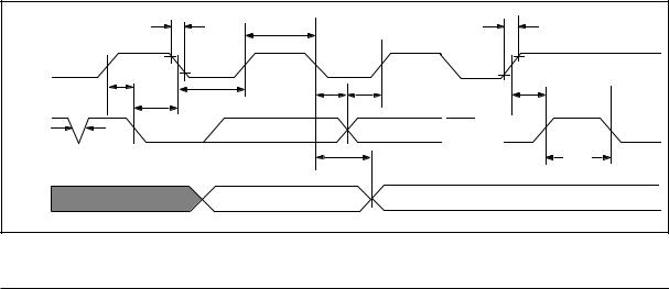
FIGURE 1-1: BUS TIMING DATA
|
TF |
THIGH |
|
TR |
|
|
|
||
|
|
|
|
|
SCL |
Tsu:sta |
|
|
|
|
|
|
|
|
|
TLOW |
THD:DAT |
TSU:DAT |
TSU:STO |
SDA |
THD:STA |
|
|
|
IN |
|
|
|
|
TSP |
|
|
|
|
|
|
|
TAA |
TBUF |
|
|
|
|
|
SDA |
|
|
|
|
OUT |
|
|
|
|
1997 Microchip Technology Inc. |
Preliminary |
DS21226A-page 3 |

24LCS61/62
2.0PIN DESCRIPTIONS
2.1SDA (Serial Data)
This is a bi-directional pin used to transfer addresses and data into and data out of the device. It is an open drain terminal, therefore the SDA bus requires a pull-up resistor to VCC (typical 10 kΩ for 100 kHz, 2 kΩ for 400 kHz).
For normal data transfer SDA is allowed to change only during SCL low. Changes during SCL high are reserved for indicating the START and STOP conditions. The SDA pin has Schmitt trigger and filter circuits which suppress noise spikes to assure proper device operation even on a noisy bus
2.2SCL (Serial Clock)
This input is used to synchronize the data transfer from and to the device. The SCL pin has Schmitt trigger and filter circuits which suppress noise spikes to assure proper device operation even on a noisy bus.
2.3EDS (External Device Select)
The External Device Select (EDS) pin is an open drain output that is controlled by using the OE bit in the control byte. It can be used to enable other circuitry when the device is selected. A pull-up resistor must be added to this pin for proper operation. This pin should not be pulled up to a voltage higher than Vcc+1V. See Section 9.0 for more details.
3.0BUS CHARACTERISTICS
The following bus protocol has been defined:
•Data transfer may be initiated only when the bus is not busy.
•During data transfer, the data line must remain stable whenever the clock line is HIGH. Changes in the data line while the clock line is HIGH will be interpreted as a START or STOP condition.
Accordingly, the following bus conditions have been defined (Figure 3-1).
3.1Bus not Busy (A)
Both data and clock lines remain HIGH.
3.2Start Data Transfer (B)
A HIGH to LOW transition of the SDA line while the clock (SCL) is HIGH determines a START condition. All commands must be preceded by a START condition.
3.3Stop Data Transfer (C)
A LOW to HIGH transition of the SDA line while the clock (SCL) is HIGH determines a STOP condition. All operations must be ended with a STOP condition.
3.4Data Valid (D)
The state of the data line represents valid data when, after a START condition, the data line is stable for the duration of the HIGH period of the clock signal.
The data on the line must be changed during the LOW period of the clock signal. There is one bit of data per clock pulse.
Each data transfer is initiated with a START condition and terminated with a STOP condition. The number of data bytes transferred between the START and STOP conditions is determined by the master device and is theoretically unlimited, although only the last sixteen will be stored when doing a write operation. When an overwrite does occur it will replace data in a first in first out fashion.
FIGURE 3-1: DATA TRANSFER SEQUENCE ON THE SERIAL BUS
SCL |
(A) |
(B) |
(D) |
(D) |
(C) |
(A) |
|
|
|
|
|
|
|
SDA |
|
|
|
|
|
|
|
|
START |
DATA OR |
DATA |
STOP |
|
|
|
CONDITION |
ACKNOWLEDGE |
ALLOWED |
CONDITION |
|
|
|
|
VALID |
TO CHANGE |
|
|
DS21226A-page 4 |
Preliminary |
1997 Microchip Technology Inc. |

24LCS61/62
3.5Acknowledge
Each receiving device, when addressed, is required to generate an acknowledge after the reception of each byte. The master device must generate an extra clock pulse which is associated with this acknowledge bit.
Note: The 24LCS61/62 does not generate any acknowledge bits if an internal programming cycle is in progress.
The device that acknowledges has to pull down the SDA line during the acknowledge clock pulse in such a way that the SDA line is stable LOW during the HIGH period of the acknowledge related clock pulse. Of course, setup and hold times must be taken into account. A master must signal an end of data to the slave by not generating an acknowledge bit on the last byte that has been clocked out of the slave. In this case, the slave must leave the data line HIGH to enable the master to generate the STOP condition (Figure 3-2).
FIGURE 3-2: |
ACKNOWLEDGE TIMING |
|
|
|
|
|
|
|
|
|
|
|||||
|
|
|
|
|
|
|
|
|
Acknowledge |
|
|
|
|
|
||
|
|
|
|
|
|
|
|
|
|
Bit |
|
|
|
|
|
|
SCL |
1 |
2 |
3 |
4 |
5 |
6 |
7 |
8 |
9 |
|
1 |
2 |
3 |
|
|
|
SDA |
|
|
|
|
|
|
|
|
|
|
|
|
|
|||
|
|
|
|
|
|
|
|
|
|
|
|
|
|
|
||
|
|
|
Data from transmitter |
|
|
|
|
|
|
Data from transmitter |
|
|
||||
|
|
|
|
|
|
|
|
|
|
|
|
|
|
|
|
|
Transmitter must release the SDA line at this point allowing the Receiver to pull the SDA line low to acknowledge the previous eight bits of data.
Receiver must release the SDA line at this point so the Transmitter can continue sending data.
1997 Microchip Technology Inc. |
Preliminary |
DS21226A-page 5
 Loading...