


Microchip Technology Inc PIC16C73-JW, PIC16C73A-04ISO, PIC16C72-JW, PIC16C72A-04-SO, PIC16C72A-04-SP Datasheet
...PIC16C7X
8-Bit CMOS Microcontrollers with A/D Converter
Devices included in this data sheet:
• |
PIC16C72 |
• |
PIC16C74A |
• |
PIC16C73 |
• |
PIC16C76 |
• |
PIC16C73A |
• |
PIC16C77 |
• |
PIC16C74 |
|
|
PIC16C7X Microcontroller Core Features:
•High-performance RISC CPU
•Only 35 single word instructions to learn
•All single cycle instructions except for program branches which are two cycle
•Operating speed: DC - 20 MHz clock input
DC - 200 ns instruction cycle
•Up to 8K x 14 words of Program Memory, up to 368 x 8 bytes of Data Memory (RAM)
•Interrupt capability
•Eight level deep hardware stack
•Direct, indirect, and relative addressing modes
•Power-on Reset (POR)
•Power-up Timer (PWRT) and Oscillator Start-up Timer (OST)
•Watchdog Timer (WDT) with its own on-chip RC oscillator for reliable operation
•Programmable code-protection
•Power saving SLEEP mode
•Selectable oscillator options
•Low-power, high-speed CMOS EPROM technology
•Fully static design
•Wide operating voltage range: 2.5V to 6.0V
•High Sink/Source Current 25/25 mA
•Commercial, Industrial and Extended temperature ranges
•Low-power consumption:
•< 2 mA @ 5V, 4 MHz
•15 A typical @ 3V, 32 kHz
•< 1 A typical standby current
PIC16C7X Peripheral Features:
•Timer0: 8-bit timer/counter with 8-bit prescaler
•Timer1: 16-bit timer/counter with prescaler, can be incremented during sleep via external crystal/clock
•Timer2: 8-bit timer/counter with 8-bit period register, prescaler and postscaler
•Capture, Compare, PWM module(s)
•Capture is 16-bit, max. resolution is 12.5 ns, Compare is 16-bit, max. resolution is 200 ns, PWM max. resolution is 10-bit
•8-bit multichannel analog-to-digital converter
•Synchronous Serial Port (SSP) with SPI and I2C
•Universal Synchronous Asynchronous Receiver Transmitter (USART/SCI)
•Parallel Slave Port (PSP) 8-bits wide, with external RD, WR and CS controls
•Brown-out detection circuitry for Brown-out Reset (BOR)
PIC16C7X Features |
72 |
73 |
73A |
74 |
74A |
76 |
77 |
|
|
|
|
|
|
|
|
|
|
|
|
|
|
|
|
Program Memory (EPROM) x 14 |
2K |
4K |
4K |
4K |
4K |
8K |
8K |
|
|
|
|
|
|
|
|
Data Memory (Bytes) x 8 |
128 |
192 |
192 |
192 |
192 |
368 |
368 |
|
|
|
|
|
|
|
|
I/O Pins |
22 |
22 |
22 |
33 |
33 |
22 |
33 |
|
|
|
|
|
|
|
|
Parallel Slave Port |
— |
— |
— |
Yes |
Yes |
— |
Yes |
|
|
|
|
|
|
|
|
Capture/Compare/PWM Modules |
1 |
2 |
2 |
2 |
2 |
2 |
2 |
|
|
|
|
|
|
|
|
Timer Modules |
3 |
3 |
3 |
3 |
3 |
3 |
3 |
|
|
|
|
|
|
|
|
A/D Channels |
5 |
5 |
5 |
8 |
8 |
5 |
8 |
|
|
|
|
|
|
|
|
Serial Communication |
SPI/I2C |
SPI/I2C, |
SPI/I2C, |
SPI/I2C, |
SPI/I2C, |
SPI/I2C, |
SPI/I2C, |
|
|
USART |
USART |
USART |
USART |
USART |
USART |
|
|
|
|
|
|
|
|
In-Circuit Serial Programming |
Yes |
Yes |
Yes |
Yes |
Yes |
Yes |
Yes |
|
|
|
|
|
|
|
|
Brown-out Reset |
Yes |
— |
Yes |
— |
Yes |
Yes |
Yes |
|
|
|
|
|
|
|
|
Interrupt Sources |
8 |
11 |
11 |
12 |
12 |
11 |
12 |
|
|
|
|
|
|
|
|
|
|
|
|
|
|
|
|
|
|
|
|
|
|
|
|
1997 Microchip Technology Inc. |
|
|
|
|
|
DS30390E-page 1 |
|
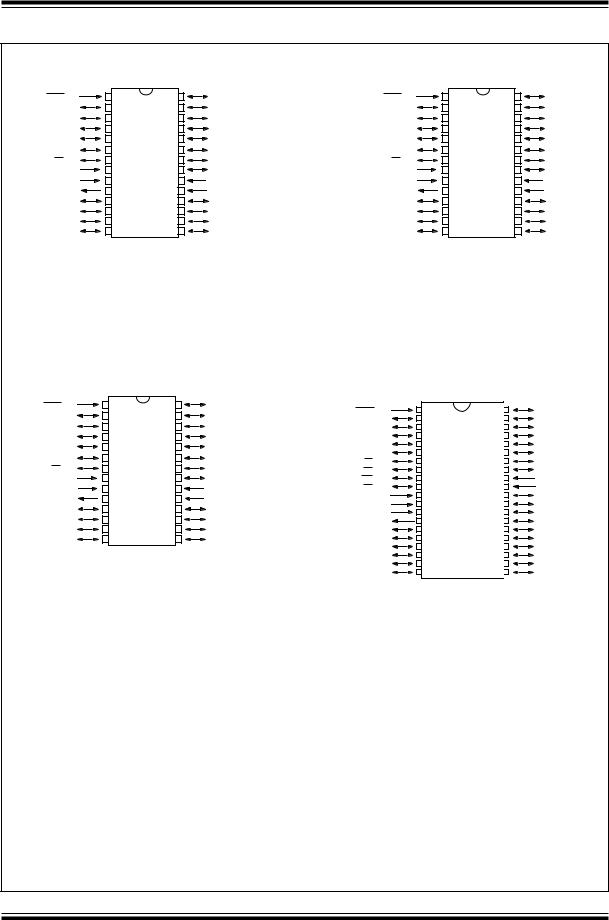
PIC16C7X
Pin Diagrams
SDIP, SOIC, Windowed Side Brazed Ceramic
MCLR/VPP |
• 1 |
28 |
RB7 |
RA0/AN0 |
2 |
27 |
RB6 |
RA1/AN1 |
3 |
26 |
RB5 |
RA2/AN2 |
4 |
25 |
RB4 |
RA3/AN3/VREF |
5 |
24 |
RB3 |
RA4/T0CKI |
6 |
23 |
RB2 |
RA5/SS/AN4 |
7 |
22 |
RB1 |
VSS |
8 |
21 |
RB0/INT |
OSC1/CLKIN |
9 |
20 |
VDD |
OSC2/CLKOUT |
10 |
19 |
VSS |
RC0/T1OSO/T1CKI |
11 |
18 |
RC7 |
RC1/T1OSI |
12 |
17 |
RC6 |
RC2/CCP1 |
13 |
16 |
RC5/SDO |
RC3/SCK/SCL |
14 |
15 |
RC4/SDI/SDA |
PIC16C72
SDIP, SOIC, Windowed Side Brazed Ceramic
MCLR/VPP |
• 1 |
28 |
RB7 |
RA0/AN0 |
2 |
27 |
RB6 |
RA1/AN1 |
3 |
26 |
RB5 |
RA2/AN2 |
4 |
25 |
RB4 |
RA3/AN3/VREF |
5 |
24 |
RB3 |
RA4/T0CKI |
6 |
23 |
RB2 |
RA5/SS/AN4 |
7 |
22 |
RB1 |
VSS |
8 |
21 |
RB0/INT |
OSC1/CLKIN |
9 |
20 |
VDD |
OSC2/CLKOUT |
10 |
19 |
VSS |
RC0/T1OSO/T1CKI |
11 |
18 |
RC7/RX/DT |
RC1/T1OSI/CCP2 |
12 |
17 |
RC6/TX/CK |
RC2/CCP1 |
13 |
16 |
RC5/SDO |
RC3/SCK/SCL |
14 |
15 |
RC4/SDI/SDA |
PIC16C73
PIC16C73A
PIC16C76
SSOP
MCLR/VPP |
• 1 |
28 |
RB7 |
RA0/AN0 |
2 |
27 |
RB6 |
RA1/AN1 |
3 |
26 |
RB5 |
RA2/AN2 |
4 |
25 |
RB4 |
RA3/AN3/VREF |
5 |
24 |
RB3 |
RA4/T0CKI |
6 |
23 |
RB2 |
RA5/SS/AN4 |
7 |
22 |
RB1 |
VSS |
8 |
21 |
RB0/INT |
OSC1/CLKIN |
9 |
20 |
VDD |
OSC2/CLKOUT |
10 |
19 |
VSS |
RC0/T1OSO/T1CKI |
11 |
18 |
RC7 |
RC1/T1OSI |
12 |
17 |
RC6 |
RC2/CCP1 |
13 |
16 |
RC5/SDO |
RC3/SCK/SCL |
14 |
15 |
RC4/SDI/SDA |
PIC16C72
PDIP, Windowed CERDIP
MCLR/VPP |
1 |
40 |
RB7 |
RA0/AN0 |
2 |
39 |
RB6 |
RA1/AN1 |
3 |
38 |
RB5 |
RA2/AN2 |
4 |
37 |
RB4 |
RA3/AN3/VREF |
5 |
36 |
RB3 |
RA4/T0CKI |
6 |
35 |
RB2 |
RA5/SS/AN4 |
7 |
34 |
RB1 |
RE0/RD/AN5 |
8 |
33 |
RB0/INT |
RE1/WR/AN6 |
9 |
32 |
VDD |
RE2/CS/AN7 |
10 |
31 |
VSS |
VDD |
11 |
30 |
RD7/PSP7 |
VSS |
12 |
29 |
RD6/PSP6 |
OSC1/CLKIN |
13 |
28 |
RD5/PSP5 |
OSC2/CLKOUT |
14 |
27 |
RD4/PSP4 |
RC0/T1OSO/T1CKI |
15 |
26 |
RC7/RX/DT |
RC1/T1OSI/CCP2 |
16 |
25 |
RC6/TX/CK |
RC2/CCP1 |
17 |
24 |
RC5/SDO |
RC3/SCK/SCL |
18 |
23 |
RC4/SDI/SDA |
RD0/PSP0 |
19 |
22 |
RD3/PSP3 |
RD1/PSP1 |
20 |
21 |
RD2/PSP2 |
PIC16C74
PIC16C74A
PIC16C77
DS30390E-page 2 |
1997 Microchip Technology Inc. |
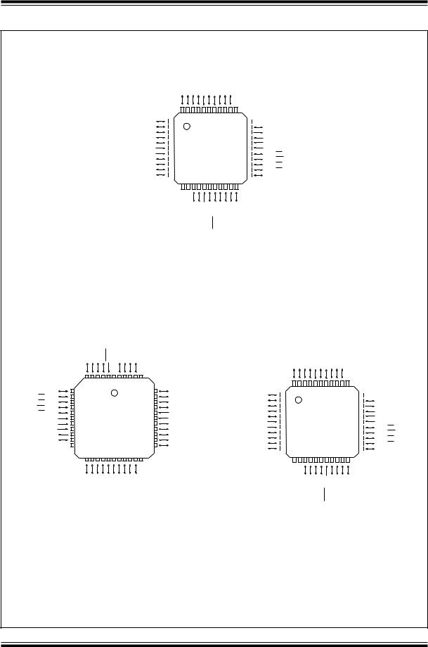
PIC16C7X
Pin Diagrams (Cont.’d)
|
|
|
|
|
|
|
|
|
|
MQFP |
|
RC6/TX/CK |
|
RC4/SDI/SDA |
|
|
|
|
RC3/SCK/SCL |
|
RC1/T1OSI/CCP2 |
|
|
|
|
|
|
|
|
|
|
|
|
|
|
|
|
|
|
|
|
|
|
|
|
|
|
|
|
|
|
RC5/SDO |
RD3/PSP3 |
RD2/PSP2 |
RD1/PSP1 |
RD0/PSP0 |
RC2/CCP1 |
NC |
|
|
|
|
|
|
|
|
|
|
|
|
|
|
|
||||
|
|
|
|
|
|
|
|
|
RC7/RX/DT |
1 |
44 |
43 |
42 |
41 |
40 |
39 |
38 37 |
36 |
35 |
34 |
33 |
NC |
|
|
|
|
|
|
|
|
|
|
|
|
|
|||
|
|
|
|
|
|
|
|
|
|
|
|
|
|
|
|
|
|
|
|
|
|
|
|
|
|
|
|
|
|
|
|
|
||||||
|
|
|
|
|
|
|
|
|
RD4/PSP4 |
2 |
|
|
|
|
|
|
|
|
|
|
|
32 |
RC0/T1OSO/T1CKI |
|
|
|
|
|
|
|
|
|
|
|||||
|
|
|
|
|
|
|
|
|
RD5/PSP5 |
3 |
|
|
|
|
|
|
|
|
|
|
|
31 |
OSC2/CLKOUT |
|
|
|
|
|
|
|
|
|
|
|
|
|||
|
|
|
|
|
|
|
|
|
RD6/PSP6 |
4 |
|
|
|
|
|
|
|
|
|
|
|
30 |
OSC1/CLKIN |
|
|
|
|
|
|
|
|
|
|
|
|
|||
|
|
|
|
|
|
|
|
|
RD7/PSP7 |
5 |
|
|
|
|
|
|
|
|
|
|
|
29 |
VSS |
|
|
|
|
|
|
|
|
|
|
|
|
|
||
|
|
|
|
|
|
|
|
|
|
|
VSS |
6 |
|
PIC16C74 |
|
28 |
VDD |
|
|
|
|
|
|
|
|
|
|
|
|
|
||||||||
|
|
|
|
|
|
|
|
|
|
|
VDD |
7 |
|
|
27 |
RE2/CS/AN7 |
|
|
|
|
|
|
|
|
|
|
|
|
||||||||||
|
|
|
|
|
|
|
|
|
|
RB0/INT |
8 |
|
|
|
|
|
|
|
|
|
|
|
26 |
RE1/WR/AN6 |
|
|
|
|
|
|
|
|
|
|
|
|
||
|
|
|
|
|
|
|
|
|
|
|
RB1 |
9 |
|
|
|
|
|
|
|
|
|
|
|
25 |
RE0/RD/AN5 |
|
|
|
|
|
|
|
|
|
|
|
|
|
|
|
|
|
|
|
|
|
|
|
|
RB2 |
10 |
|
|
|
|
|
|
|
|
|
|
24 |
RA5/SS/AN4 |
|
|
|
|
|
|
|
|
|
|
|
|
|
|
|
|
|
|
|
|
|
|
|
|
|
RB3 |
11 |
|
|
|
|
|
|
|
|
|
|
23 |
RA4/T0CKI |
|
|
|
|
|
|
|
|
|
|
|
|
|
|
|
|
|
|
|
|
|
|
|
|
|
|
|
12 |
13 |
14 |
15 |
16 |
17 |
18 |
19 |
20 |
21 |
22 |
|
|
|
|
|
|
|
|
|
|
|
|
|
|
|
|
|
|
|
|
|
|
|
|
|
|
|
|
NC NC |
RB4 |
RB5 |
RB6 |
RB7 |
MCLR/VPP |
RA0/AN0 |
RA1/AN1 |
RA2/AN2 |
RA3/AN3/VREF |
|
|
|
|
|
|
|
|
|
|
|
|
|
|
|
|
PLCC |
RA3/AN3/VREF |
RA2/AN2 |
RA1/AN1 |
RA0/AN0 |
MCLR/VPP |
|
|
|
|
|
|
|
|
|
|
|
|
|
|
|
|
|
|
|
|
RC6/TX/CK |
RC5/SDO |
RC4/SDI/SDA |
RD3/PSP3 |
RD2/PSP2 |
RD1/PSP1 |
RD0/PSP0 |
RC3/SCK/SCL |
RC2/CCP1 |
RC1/T1OSI/CCP2 |
|
|
|
|
NC |
RB7 |
RB6 |
RB5 |
RB4 |
NC |
|
|
|
|
|
|
|
|
|
|
|
|
MQFP |
|
|
|
|
|||||||||||||||
|
|
|
|
|
|
|
|
|
|
|
|
|
TQFP |
|
NC |
|
|
|||||||||||||||||||||
|
6 5 4 3 |
2 1 |
44 43 |
42 41 |
40 |
|
|
|
|
|
|
|
|
|
|
|
|
|
|
|
|
|
|
|
|
|
|
|
|
|
|
|
||||||
RA4/T0CKI |
7 |
|
|
|
|
|
|
|
|
|
39 |
RB3 |
|
|
|
|
|
|
|
|
|
|
|
RC7/RX/DT |
1 |
44 43 42 41 40 39 |
38 37 |
36 35 |
34 |
33 |
NC |
|||||||
RA5/SS/AN4 |
8 |
|
|
|
|
|
|
|
|
|
38 |
RB2 |
|
|
|
|
|
|
|
|
|
|
|
|
|
|
|
|
|
|
|
|
|
|
||||
|
|
|
|
|
|
|
|
|
|
|
|
|
|
|
|
|
|
|
|
RD4/PSP4 |
2 |
|
|
|
|
|
|
|
|
|
|
|
32 |
RC0/T1OSO/T1CKI |
||||
RE0/RD/AN5 |
9 |
|
|
|
|
|
|
|
|
|
37 |
RB1 |
|
|
|
|
|
|
|
|
|
|
|
|
|
|
|
|
|
|
|
|
|
|
||||
|
|
|
|
|
|
|
|
|
|
|
|
|
|
|
|
|
|
|
|
RD5/PSP5 |
3 |
|
|
|
|
|
|
|
|
|
|
|
31 |
OSC2/CLKOUT |
||||
RE1/WR/AN6 |
10 |
PIC16C74 |
36 |
RB0/INT |
|
|
|
|
|
|
|
|
|
|
|
|
|
|
|
|
|
|
|
|
||||||||||||||
|
|
|
|
|
|
|
|
|
RD6/PSP6 |
4 |
|
|
|
|
|
|
|
|
|
|
|
30 |
OSC1/CLKIN |
|||||||||||||||
RE2/CS/AN7 |
11 |
35 |
VDD |
|
|
|
|
|
|
|
|
|
|
|
|
|
|
|
|
|
|
|
|
|
|
|||||||||||||
VDD |
12 |
PIC16C74A |
34 |
VSS |
|
|
|
|
|
|
|
|
|
|
|
RD7/PSP7 |
5 |
|
PIC16C74A 29 |
VSS |
||||||||||||||||||
VSS |
13 |
33 |
RD7/PSP7 |
|
|
|
|
|
|
|
|
VSS |
6 |
|
|
PIC16C77 |
|
28 |
VDD |
|||||||||||||||||||
OSC1/CLKIN |
14 |
PIC16C77 |
32 |
RD6/PSP6 |
|
|
|
|
|
|
|
|
VDD |
7 |
|
|
|
27 |
RE2/CS/AN7 |
|||||||||||||||||||
|
|
|
|
|
|
|
|
RB0/INT |
8 |
|
|
|
26 |
RE1/WR/AN6 |
||||||||||||||||||||||||
OSC2/CLKOUT |
15 |
31 |
RD5/PSP5 |
|
|
|
|
|
|
|
|
|
|
|
||||||||||||||||||||||||
|
|
|
|
|
|
|
|
RB1 |
9 |
|
|
|
|
|
|
|
|
|
|
|
25 |
RE0/RD/AN5 |
||||||||||||||||
RC0/T1OSO/T1CKI |
16 |
|
|
|
|
|
|
|
|
|
30 |
RD4/PSP4 |
|
|
|
|
|
|
|
|
|
|
|
|
|
|
|
|
|
|
|
|||||||
|
|
|
|
|
|
|
|
|
|
|
|
|
|
|
|
|
RB2 |
10 |
|
|
|
|
|
|
|
|
|
|
24 |
RA5/SS/AN4 |
||||||||
NC |
17 |
|
|
|
|
|
|
|
|
|
29 |
RC7/RX/DT |
|
|
|
|
|
|
|
|
|
|
|
|
|
|
|
|
|
|
||||||||
|
|
|
|
|
|
|
|
|
|
|
|
|
|
|
|
|
RB3 |
11 |
|
|
|
|
|
|
|
|
|
|
23 |
RA4/T0CKI |
||||||||
|
|
|
|
|
|
|
|
|
|
|
|
|
|
|
|
|
|
|
|
|
|
|
|
|
|
|
|
|
|
|
|
|
|
|||||
|
18 |
19 |
20 |
21 |
22 |
23 |
24 |
25 |
26 |
27 |
28 |
|
|
|
|
|
|
|
|
|
|
|
|
|
|
12 |
13 |
14 |
15 |
16 |
17 |
18 |
19 |
20 |
21 |
22 |
|
|
|
RC1/T1OSI/CCP2 |
RC2/CCP1 |
RC3/SCK/SCL |
RD0/PSP0 |
RD1/PSP1 |
RD2/PSP2 |
RD3/PSP3 |
RC4/SDI/SDA |
RC5/SDO |
RC6/TX/CK |
NC |
|
|
|
|
|
|
|
|
|
|
|
|
|
|
NC |
NC |
RB4 |
RB5 |
RB6 |
RB7 |
MCLR/VPP |
RA0/AN0 |
RA1/AN1 |
RA2/AN2 |
RA3/AN3/VREF |
|
|
1997 Microchip Technology Inc. |
DS30390E-page 3 |
PIC16C7X |
|
||
Table of Contents |
|
||
1.0 |
General Description ....................................................................................................................................................................... |
5 |
|
2.0 |
PIC16C7X Device Varieties ........................................................................................................................................................... |
7 |
|
3.0 |
Architectural Overview ................................................................................................................................................................... |
9 |
|
4.0 |
Memory Organization................................................................................................................................................................... |
19 |
|
5.0 |
I/O Ports |
....................................................................................................................................................................................... |
43 |
6.0 |
Overview .........................................................................................................................................................of Timer Modules |
57 |
|
7.0 |
Timer0 Module ............................................................................................................................................................................. |
59 |
|
8.0 |
Timer1 Module ............................................................................................................................................................................. |
65 |
|
9.0 |
Timer2 Module ............................................................................................................................................................................. |
69 |
|
10.0 |
Capture/Compare/PWM ..............................................................................................................................................Module(s) |
71 |
|
11.0 |
Synchronous .......................................................................................................................................Serial Port (SSP) Module |
77 |
|
12.0 |
Universal ......................................................................................Synchronous Asynchronous Receiver Transmitter (USART) |
99 |
|
13.0 |
Analog-to .................................................................................................................................-Digital Converter (A/D) Module |
117 |
|
14.0 |
Special Features .....................................................................................................................................................of the CPU |
129 |
|
15.0 |
Instruction ............................................................................................................................................................Set Summary |
147 |
|
16.0 |
Development ................................................................................................................................................................Support |
163 |
|
17.0 |
Electrical .....................................................................................................................................Characteristics for PIC16C72 |
167 |
|
18.0 |
Electrical ................................................................................................................................Characteristics for PIC16C73/74 |
183 |
|
19.0 |
Electrical ...........................................................................................................................Characteristics for PIC16C73A/74A |
201 |
|
20.0 |
Electrical ................................................................................................................................Characteristics for PIC16C76/77 |
219 |
|
21.0 |
DC and AC ........................................................................................................................Characteristics Graphs and Tables |
241 |
|
22.0 |
Packaging ...............................................................................................................................................................Information |
251 |
|
Appendix A: ................................................................................................................................................................................... |
|
263 |
|
Appendix B: ............................................................................................................................................................. |
Compatibility |
263 |
|
Appendix C: ............................................................................................................................................................... |
What’s New |
264 |
|
Appendix D: ....................................................................................................................................................... |
What’s Changed |
264 |
|
Appendix E: ....................................................................................................................................... |
PIC16/17 Microcontrollers |
265 |
|
Pin Compatibility ................................................................................................................................................................................ |
271 |
||
Index .................................................................................................................................................................................................. |
|
273 |
|
List of Examples................................................................................................................................................................................. |
279 |
||
List of Figures..................................................................................................................................................................................... |
|
280 |
|
List of Tables...................................................................................................................................................................................... |
|
283 |
|
Reader Response .............................................................................................................................................................................. |
286 |
||
PIC16C7X Product ...........................................................................................................................................Identification System |
287 |
||
For register and module descriptions in this data sheet, device legends show which devices apply to those sections. As an example, the legend below would mean that the following section applies only to the PIC16C72, PIC16C73A and PIC16C74A devices.
Applicable Devices
72 73 73A 74 74A 76 77
To Our Valued Customers
We constantly strive to improve the quality of all our products and documentation. We have spent an exceptional amount of time to ensure that these documents are correct. However, we realize that we may have missed a few things. If you find any information that is missing or appears in error, please use the reader response form in the back of this data sheet to inform us. We appreciate your assistance in making this a better document.
DS30390E-page 4 |
1997 Microchip Technology Inc. |

PIC16C7X
1.0GENERAL DESCRIPTION
The PIC16C7X is a family of low-cost, high-perfor- mance, CMOS, fully-static, 8-bit microcontrollers with integrated analog-to-digital (A/D) converters, in the PIC16CXX mid-range family.
All PIC16/17 microcontrollers employ an advanced RISC architecture. The PIC16CXX microcontroller family has enhanced core features, eight-level deep stack, and multiple internal and external interrupt sources. The separate instruction and data buses of the Harvard architecture allow a 14-bit wide instruction word with the separate 8-bit wide data. The two stage instruction pipeline allows all instructions to execute in a single cycle, except for program branches which require two cycles. A total of 35 instructions (reduced instruction set) are available. Additionally, a large register set gives some of the architectural innovations used to achieve a very high performance.
PIC16CXX microcontrollers typically achieve a 2:1 code compression and a 4:1 speed improvement over other 8-bit microcontrollers in their class.
The PIC16C72 has 128 bytes of RAM and 22 I/O pins. In addition several peripheral features are available including: three timer/counters, one Capture/Compare/ PWM module and one serial port. The Synchronous Serial Port can be configured as either a 3-wire Serial Peripheral Interface (SPI) or the two-wire Inter-Inte- grated Circuit (I2C) bus. Also a 5-channel high-speed 8-bit A/D is provided. The 8-bit resolution is ideally suited for applications requiring low-cost analog interface, e.g. thermostat control, pressure sensing, etc.
The PIC16C73/73A devices have 192 bytes of RAM, while the PIC16C76 has 368 byes of RAM. Each device has 22 I/O pins. In addition, several peripheral features are available including: three timer/counters, two Capture/Compare/PWM modules and two serial ports. The Synchronous Serial Port can be configured as either a 3-wire Serial Peripheral Interface (SPI) or the two-wire Inter-Integrated Circuit (I2C) bus. The Universal Synchronous Asynchronous Receiver Transmitter (USART) is also known as the Serial Communications Interface or SCI. Also a 5-channel high-speed 8-bit A/ D is provided.The 8-bit resolution is ideally suited for applications requiring low-cost analog interface, e.g. thermostat control, pressure sensing, etc.
The PIC16C74/74A devices have 192 bytes of RAM, while the PIC16C77 has 368 bytes of RAM. Each device has 33 I/O pins. In addition several peripheral features are available including: three timer/counters, two Capture/Compare/PWM modules and two serial ports. The Synchronous Serial Port can be configured as either a 3-wire Serial Peripheral Interface (SPI) or the two-wire Inter-Integrated Circuit (I2C) bus. The Universal Synchronous Asynchronous Receiver Transmitter (USART) is also known as the Serial Communications Interface or SCI. An 8-bit Parallel Slave Port is provided. Also an 8-channel high-speed
8-bit A/D is provided. The 8-bit resolution is ideally suited for applications requiring low-cost analog interface, e.g. thermostat control, pressure sensing, etc.
The PIC16C7X family has special features to reduce external components, thus reducing cost, enhancing system reliability and reducing power consumption. There are four oscillator options, of which the single pin RC oscillator provides a low-cost solution, the LP oscillator minimizes power consumption, XT is a standard crystal, and the HS is for High Speed crystals. The SLEEP (power-down) feature provides a power saving mode. The user can wake up the chip from SLEEP through several external and internal interrupts and resets.
A highly reliable Watchdog Timer with its own on-chip RC oscillator provides protection against software lockup.
A UV erasable CERDIP packaged version is ideal for code development while the cost-effective One-Time- Programmable (OTP) version is suitable for production in any volume.
The PIC16C7X family fits perfectly in applications ranging from security and remote sensors to appliance control and automotive. The EPROM technology makes customization of application programs (transmitter codes, motor speeds, receiver frequencies, etc.) extremely fast and convenient. The small footprint packages make this microcontroller series perfect for all applications with space limitations. Low cost, low power, high performance, ease of use and I/O flexibility make the PIC16C7X very versatile even in areas where no microcontroller use has been considered before (e.g. timer functions, serial communication, capture and compare, PWM functions and coprocessor applications).
1.1Family and Upward Compatibility
Users familiar with the PIC16C5X microcontroller family will realize that this is an enhanced version of the PIC16C5X architecture. Please refer to Appendix A for a detailed list of enhancements. Code written for the PIC16C5X can be easily ported to the PIC16CXX family of devices (Appendix B).
1.2Development Support
PIC16C7X devices are supported by the complete line of Microchip Development tools.
Please refer to Section 16.0 for more details about Microchip’s development tools.
1997 Microchip Technology Inc. |
DS30390E-page 5 |

PIC16C7X
TABLE 1-1: |
PIC16C7XX FAMILY OF DEVCES |
|
|
|
|
|
|
|
|
|
|
|
|
|
|
||||||
|
|
|
|
|
|
|
|
|
|
|
|
|
|
|
|
|
|
|
|
|
|
|
|
|
|
|
PIC16C710 |
|
PIC16C71 |
|
|
PIC16C711 |
|
PIC16C715 |
|
PIC16C72 |
|
PIC16CR72(1) |
|
||||
|
Clock |
Maximum Frequency |
20 |
|
20 |
|
|
|
|
20 |
|
|
20 |
|
20 |
|
|
20 |
|
||
|
of Operation (MHz) |
|
|
|
|
|
|
|
|
|
|
|
|
|
|
|
|
|
|||
|
|
|
|
|
|
|
|
|
|
|
|
|
|
|
|
|
|
|
|||
|
|
|
|
|
|
|
|
|
|
|
|
|
|
|
|
|
|
|
|
|
|
|
|
EPROM Program Memory |
512 |
|
1K |
|
|
|
|
1K |
|
|
2K |
|
2K |
|
|
— |
|
||
|
|
(x14 words) |
|
|
|
|
|
|
|
|
|
|
|
|
|
|
|
|
|
||
|
Memory |
|
|
|
|
|
|
|
|
|
|
|
|
|
|
|
|
|
|
|
|
|
ROM Program Memory |
— |
— |
|
|
— |
|
|
— |
|
— |
|
|
2K |
|
|
|
||||
|
|
(14K words) |
|
|
|
|
|
|
|
|
|
|
|
|
|
|
|
|
|
||
|
|
|
|
|
|
|
|
|
|
|
|
|
|
|
|
|
|
|
|
||
|
|
Data Memory (bytes) |
36 |
36 |
|
|
|
|
68 |
|
|
128 |
|
128 |
|
|
128 |
|
|||
|
|
|
|
|
|
|
|
|
|
|
|
|
|
|
|
|
|
|
|
|
|
|
|
Timer Module(s) |
TMR0 |
|
TMR0 |
|
|
TMR0 |
|
|
TMR0 |
|
TMR0, |
|
|
TMR0, |
|
||||
|
|
|
|
|
|
|
|
|
|
|
|
|
|
|
|
|
TMR1, |
|
|
TMR1, |
|
|
|
|
|
|
|
|
|
|
|
|
|
|
|
|
|
|
TMR2 |
|
|
TMR2 |
|
|
|
|
|
|
|
|
|
|
|
|
|
|
|
|
|
|
|
|
|
||
|
Peripherals |
Capture/Compare/ |
— |
— |
|
|
— |
|
|
— |
|
1 |
|
|
1 |
|
|
|
|||
|
PWM Module(s) |
|
|
|
|
|
|
|
|
|
|
|
|
|
|
|
|
|
|||
|
|
|
|
|
|
|
|
|
|
|
|
|
|
|
|
|
|
|
|||
|
|
Serial Port(s) |
— |
— |
|
|
— |
|
|
— |
|
SPI/I 2C |
|
|
SPI/I2C |
|
|||||
|
|
(SPI/I2C, USART) |
|
|
|
|
|
|
|
|
|
|
|
|
|
|
|
|
|
||
|
|
Parallel Slave Port |
— |
— |
|
|
— |
|
|
— |
|
— |
|
|
— |
|
|
|
|||
|
|
|
|
|
|
|
|
|
|
|
|
|
|
|
|
|
|
|
|
|
|
|
|
A/D Converter (8-bit) Channels |
4 |
4 |
|
|
|
|
4 |
|
|
4 |
5 |
|
|
5 |
|
||||
|
|
|
|
|
|
|
|
|
|
|
|
|
|
|
|
|
|
|
|
|
|
|
|
Interrupt Sources |
4 |
4 |
|
|
|
|
4 |
|
|
4 |
8 |
|
|
8 |
|
||||
|
|
|
|
|
|
|
|
|
|
|
|
|
|
|
|
|
|
|
|||
|
|
I/O Pins |
13 |
13 |
|
|
|
|
13 |
|
|
13 |
22 |
|
|
22 |
|
||||
|
|
|
|
|
|
|
|
|
|
|
|
|
|
|
|
|
|
|
|||
|
|
Voltage Range (Volts) |
3.0-6.0 |
3.0-6.0 |
|
|
3.0-6.0 |
|
|
3.0-5.5 |
2.5-6.0 |
|
|
3.0-5.5 |
|
||||||
|
|
|
|
|
|
|
|
|
|
|
|
|
|
|
|
|
|
|
|
|
|
|
Features |
In-Circuit Serial Programming |
Yes |
|
Yes |
|
|
|
|
Yes |
|
|
Yes |
|
Yes |
|
|
Yes |
|
||
|
|
|
|
|
|
|
|
|
|
|
|
|
|
|
|
|
|
|
|
|
|
|
|
Brown-out Reset |
Yes |
|
— |
|
|
|
|
Yes |
|
|
Yes |
Yes |
|
|
Yes |
|
|||
|
|
|
|
|
|
|
|
|
|
|
|
|
|
|
|
|
|
|
|
|
|
|
|
Packages |
18-pin DIP, |
|
18-pin DIP, |
|
|
18-pin DIP, |
|
|
18-pin DIP, |
|
28-pin SDIP, |
|
28-pin SDIP, |
|
|||||
|
|
|
|
|
SOIC; |
|
SOIC |
|
|
|
|
SOIC; |
|
|
SOIC; |
|
SOIC, SSOP |
|
SOIC, SSOP |
|
|
|
|
|
|
|
20-pin SSOP |
|
|
|
|
|
|
20-pin SSOP |
|
20-pin SSOP |
|
|
|
|
|
|
|
|
|
|
|
|
|
|
|
|
|
|
|
|
|
|
|
|
|
|
|||
|
|
|
|
|
|
|
|
|
|
|
|
|
|
|
|
|
|
|
|
|
|
|
|
|
|
|
PIC16C73A |
|
PIC16C74A |
|
|
PIC16C76 |
|
PIC16C77 |
|
||||||||
|
|
|
|
|
|
|
|
|
|
|
|
|
|
|
|
|
|
|
|
|
|
|
Clock |
Maximum Frequency of Oper- |
20 |
|
|
|
20 |
|
|
|
|
|
20 |
|
|
20 |
|
|
|
||
|
ation (MHz) |
|
|
|
|
|
|
|
|
|
|
|
|
|
|
|
|
|
|||
|
|
|
|
|
|
|
|
|
|
|
|
|
|
|
|
|
|
|
|||
|
|
|
|
|
|
|
|
|
|
|
|
|
|
|
|
|
|
|
|
|
|
|
|
EPROM Program Memory |
4K |
|
|
|
4K |
|
|
|
|
|
8K |
|
|
8K |
|
|
|
||
|
Memory |
(x14 words) |
|
|
|
|
|
|
|
|
|
|
|
|
|
|
|
|
|
||
|
|
Data Memory (bytes) |
192 |
|
|
|
192 |
|
|
|
|
|
368 |
|
|
368 |
|
|
|
||
|
|
|
|
|
|
|
|
|
|
|
|
|
|
|
|
|
|
|
|||
|
|
Timer Module(s) |
TMR0, |
|
|
|
TMR0, |
|
|
TMR0, |
|
|
TMR0, |
|
|||||||
|
|
|
|
|
TMR1, |
|
|
|
TMR1, |
|
|
TMR1, |
|
|
TMR1, |
|
|||||
|
|
|
|
|
TMR2 |
|
|
|
TMR2 |
|
|
TMR2 |
|
|
TMR2 |
|
|||||
|
|
|
|
|
|
|
|
|
|
|
|
|
|
|
|
|
|
|
|
||
|
Peripherals |
Capture/Compare/PWM Mod- |
2 |
|
|
|
2 |
|
|
|
|
|
2 |
|
|
2 |
|
|
|
||
|
ule(s) |
|
|
|
|
|
|
|
|
|
|
|
|
|
|
|
|
|
|
|
|
|
|
|
|
|
|
|
|
|
|
|
|
||||||||||
|
|
Serial |
Port(s) (SPI/I2C, US- |
SPI/I2C, USART |
|
SPI/I2C, USART |
|
|
SPI/I2C, USART |
SPI/I2C, USART |
|
||||||||||
|
|
ART) |
|
|
|
|
|
|
|
|
|
|
|
|
|
|
|
|
|
|
|
|
|
|
|
|
|
|
|
|
|
|
|
|
|
|
|
|
|
|
|
||
|
|
Parallel Slave Port |
— |
|
|
|
Yes |
|
|
|
|
|
— |
|
Yes |
|
|
|
|||
|
|
|
|
|
|
|
|
|
|
|
|
|
|
|
|
|
|
|
|||
|
|
A/D Converter (8-bit) Channels |
5 |
|
|
|
8 |
|
|
|
|
5 |
|
|
8 |
|
|
|
|||
|
|
Interrupt Sources |
11 |
|
|
|
12 |
|
|
|
|
11 |
|
|
12 |
|
|
|
|||
|
|
|
|
|
|
|
|
|
|
|
|
|
|
|
|
|
|
|
|||
|
|
I/O Pins |
22 |
|
|
|
33 |
|
|
|
|
22 |
|
|
33 |
|
|
|
|||
|
|
|
|
|
|
|
|
|
|
|
|
|
|
||||||||
|
|
Voltage Range (Volts) |
2.5-6.0 |
|
|
|
2.5-6.0 |
|
2.5-6.0 |
|
|
2.5-6.0 |
|
||||||||
|
|
|
|
|
|
|
|
|
|
|
|
|
|
|
|
|
|
|
|
||
|
Features |
In-Circuit Serial Programming |
Yes |
|
|
|
Yes |
|
|
|
|
|
Yes |
|
|
Yes |
|
|
|
||
|
|
|
|
|
|
|
|
|
|
|
|
|
|
|
|
|
|
|
|
|
|
|
|
Brown-out Reset |
Yes |
|
|
|
Yes |
|
|
|
|
|
Yes |
|
|
Yes |
|
|
|
||
|
|
|
|
|
|
|
|
|
|
|
|
|
|||||||||
|
|
Packages |
28-pin SDIP, |
|
|
|
40-pin DIP; |
|
|
28-pin SDIP, |
40-pin DIP; |
|
|||||||||
|
|
|
|
|
SOIC |
|
|
|
44-pin PLCC, |
|
|
SOIC |
|
|
44-pin PLCC, |
|
|||||
|
|
|
|
|
|
|
|
|
MQFP, TQFP |
|
|
|
|
|
MQFP, TQFP |
|
|||||
|
|
|
|
|
|
|
|
|
|
|
|
|
|
|
|
|
|
|
|
|
|
All PIC16/17 Family devices have Power-on Reset, selectable Watchdog Timer, selectable code protect and high I/O current capability. All PIC16C7XX Family devices use serial programming with clock pin RB6 and data pin RB7.
Note 1: Please contact your local Microchip sales office for availability of these devices.
DS30390E-page 6 |
1997 Microchip Technology Inc. |

PIC16C7X
2.0PIC16C7X DEVICE VARIETIES
A variety of frequency ranges and packaging options are available. Depending on application and production requirements, the proper device option can be selected using the information in the PIC16C7X Product Identification System section at the end of this data sheet. When placing orders, please use that page of the data sheet to specify the correct part number.
For the PIC16C7X family, there are two device “types” as indicated in the device number:
1.C, as in PIC16C74. These devices have EPROM type memory and operate over the standard voltage range.
2.LC, as in PIC16LC74. These devices have EPROM type memory and operate over an extended voltage range.
2.1UV Erasable Devices
The UV erasable version, offered in CERDIP package is optimal for prototype development and pilot programs. This version can be erased and reprogrammed to any of the oscillator modes.
|
|
Microchip's PICSTART |
Plus and PRO MATE II |
programmers both support programming of the PIC16C7X.
2.2One-Time-Programmable (OTP) Devices
The availability of OTP devices is especially useful for customers who need the flexibility for frequent code updates and small volume applications.
The OTP devices, packaged in plastic packages, permit the user to program them once. In addition to the program memory, the configuration bits must also be programmed.
2.3Quick-Turnaround-Production (QTP) Devices
Microchip offers a QTP Programming Service for factory production orders. This service is made available for users who choose not to program a medium to high quantity of units and whose code patterns have stabilized. The devices are identical to the OTP devices but with all EPROM locations and configuration options already programmed by the factory. Certain code and prototype verification procedures apply before production shipments are available. Please contact your local Microchip Technology sales office for more details.
2.4Serialized Quick-Turnaround Production (SQTPSM) Devices
Microchip offers a unique programming service where a few user-defined locations in each device are programmed with different serial numbers. The serial numbers may be random, pseudo-random, or sequential.
Serial programming allows each device to have a unique number which can serve as an entry-code, password, or ID number.
1997 Microchip Technology Inc. |
DS30390E-page 7 |

PIC16C7X
NOTES:
DS30390E-page 8 |
1997 Microchip Technology Inc. |

PIC16C7X
3.0ARCHITECTURAL OVERVIEW
The high performance of the PIC16CXX family can be attributed to a number of architectural features commonly found in RISC microprocessors. To begin with, the PIC16CXX uses a Harvard architecture, in which, program and data are accessed from separate memories using separate buses. This improves bandwidth over traditional von Neumann architecture in which program and data are fetched from the same memory using the same bus. Separating program and data buses further allows instructions to be sized differently than the 8-bit wide data word. Instruction opcodes are 14-bits wide making it possible to have all single word instructions. A 14-bit wide program memory access bus fetches a 14-bit instruction in a single cycle. A twostage pipeline overlaps fetch and execution of instructions (Example 3-1). Consequently, all instructions (35) execute in a single cycle (200 ns @ 20 MHz) except for program branches.
The table below lists program memory (EPROM) and data memory (RAM) for each PIC16C7X device.
Device |
Program |
Data Memory |
|
Memory |
|||
|
|
||
|
|
|
|
|
|
|
|
PIC16C72 |
2K x 14 |
128 x 8 |
|
PIC16C73 |
4K x 14 |
192 x 8 |
|
PIC16C73A |
4K x 14 |
192 x 8 |
|
PIC16C74 |
4K x 14 |
192 x 8 |
|
PIC16C74A |
4K x 14 |
192 x 8 |
|
PIC16C76 |
8K x 14 |
368 x 8 |
|
PIC16C77 |
8K x 14 |
386 x 8 |
The PIC16CXX can directly or indirectly address its register files or data memory. All special function registers, including the program counter, are mapped in the data memory. The PIC16CXX has an orthogonal (symmetrical) instruction set that makes it possible to carry out any operation on any register using any addressing mode. This symmetrical nature and lack of ‘special optimal situations’ make programming with the PIC16CXX simple yet efficient. In addition, the learning curve is reduced significantly.
PIC16CXX devices contain an 8-bit ALU and working register. The ALU is a general purpose arithmetic unit. It performs arithmetic and Boolean functions between the data in the working register and any register file.
The ALU is 8-bits wide and capable of addition, subtraction, shift and logical operations. Unless otherwise mentioned, arithmetic operations are two's complement in nature. In two-operand instructions, typically one operand is the working register (W register). The other operand is a file register or an immediate constant. In single operand instructions, the operand is either the W register or a file register.
The W register is an 8-bit working register used for ALU operations. It is not an addressable register.
Depending on the instruction executed, the ALU may affect the values of the Carry (C), Digit Carry (DC), and Zero (Z) bits in the STATUS register. The C and DC bits operate as a borrow bit and a digit borrow out bit, respectively, in subtraction. See the SUBLW and SUBWF instructions for examples.
1997 Microchip Technology Inc. |
DS30390E-page 9 |
PIC16C7X
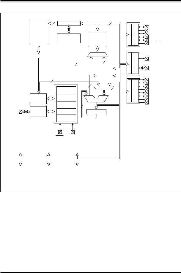
FIGURE 3-1: PIC16C72 BLOCK DIAGRAM
13 |
Data Bus |
8 |
EPROM |
Program Counter |
|
|
|
|
Program |
|
|
Memory |
RAM |
|
|
|
|
|
2K x 14 |
|
|
8 Level Stack |
|
|
|
|
|
|
|
File |
|
|
|
|
|
|
||||||||||
|
|
|
|
(13-bit) |
|
|
|
|
|
|
|
|
|
|
|
|
|
||||||||||||
|
|
|
|
|
|
|
|
|
|
Registers |
|
|
|
|
|
|
|||||||||||||
|
|
|
|
|
|
|
|
|
|
|
|
|
|
|
|
|
|
|
|
|
|||||||||
|
|
|
|
|
|
|
|
|
|
|
|
|
|
|
|
|
|
|
|
|
|
||||||||
Program |
|
|
|
|
|
|
|
|
|
|
|
|
|
|
128 x 8 |
|
|
|
|
|
|
||||||||
14 |
|
|
|
|
|
|
|
|
|
|
|
|
|
|
|||||||||||||||
|
|
|
|
|
|
|
|
|
|
|
|
|
|
|
|
|
|
|
|
|
|
|
|
|
|
|
|||
|
|
|
|
|
|
|
RAM Addr(1) |
|
|
|
|
|
9 |
|
|
|
|
|
|
|
|||||||||
Bus |
|
|
|
|
|
|
|
|
|
|
|
|
|
|
|
|
|
|
|||||||||||
|
|
|
|
|
|
|
|
|
|
|
|
|
|
|
|||||||||||||||
|
|
|
|
|
|
|
|
|
|
|
|
|
|
|
|
Addr MUX |
|
|
|
|
|
|
|||||||
|
|
Instruction reg |
|
|
|
|
|
|
|
|
|
|
|
||||||||||||||||
|
|
|
|
|
|
|
|
|
|
|
|
|
|
|
|
|
|
|
|
|
|
|
|
|
|||||
|
|
|
|
|
|
|
|
|
Direct Addr 7 |
|
|
|
|
|
|
|
8 |
|
Indirect |
||||||||||
|
|
|
|
|
|
|
|
|
|
|
|
|
|
|
|
|
|||||||||||||
|
|
|
|
|
|
|
|
|
|
|
|
|
|
|
|
|
|
|
Addr |
||||||||||
|
|
|
|
|
|
|
|
|
|
|
|
|
|
|
|
|
|
|
|||||||||||
|
|
|
|
|
|
|
|
|
|
|
|
|
|
|
|
|
|
|
|
|
|
|
|
|
|
|
|
|
|
|
|
|
|
|
|
|
|
|
|
|
|
|
|
|
|
|
|
|
|
|
|
FSR reg |
|
|
|||||
|
|
|
|
|
|
|
|
|
|
|
|
|
|
|
|
|
|
|
|
|
|
|
|
||||||
|
|
|
|
|
|
|
|
|
|
|
|
|
|
|
|
|
|
|
|
|
|
|
|
|
|
|
|
|
|
|
|
|
|
|
|
|
8 |
|
|
|
|
|
|
|
|
|
|
|
STATUS reg |
|
|
||||||||
|
|
|
|
|
|
|
|
|
|
|
|
|
|
|
|
|
|
|
|
||||||||||
|
|
|
|
|
|
|
|
|
|
|
|
|
|
|
|
|
|
|
|
|
|
|
|
|
|
|
|
||
|
|
|
|
|
|
|
|
|
|
|
|
|
|
|
|
|
|
|
|
|
|
|
|
|
|
|
|
|
|
|
|
|
|
|
|
|
|
|
|
|
|
|
|
|
|
|
|
|
|
|
|
|
|
|
|
|
|
|
|
|
Power-up |
3 |
MUX |
|
|
||
|
Timer |
|
|
Instruction |
Oscillator |
|
|
Decode & |
Start-up Timer |
|
ALU |
Control |
|
|
|
Power-on |
|
|
|
|
8 |
|
|
|
Reset |
|
|
Timing |
Watchdog |
|
W reg |
Generation |
Timer |
|
|
|
|
||
OSC1/CLKIN |
Brown-out |
|
|
OSC2/CLKOUT |
Reset |
|
|
PORTA
RA0/AN0
RA1/AN1
RA2/AN2
RA3/AN3/VREF
RA4/T0CKI
RA5/SS/AN4
PORTB
RB0/INT
RB7:RB1
PORTC
RC0/T1OSO/T1CKI
RC1/T1OSI
RC2/CCP1
RC3/SCK/SCL
RC4/SDI/SDA
RC5/SDO
RC6 RC7
MCLR VDD, VSS
Timer0 |
|
Timer1 |
|
Timer2 |
|
||||||
|
|
|
|
|
|
|
|
|
|
|
|
|
|
|
|
|
|
|
|
|
|
|
|
|
|
|
|
|
|
|
|
|
|
|
|
|
|
|
|
|
|
|
|
|
|
|
|
|
|
|
|
|
|
|
|
|
|
|
|
A/D |
|
Synchronous |
|
CCP1 |
|
Serial Port |
|
||
|
|
|
|
|
|
|
|
|
|
Note 1: Higher order bits are from the STATUS register.
DS30390E-page 10 |
1997 Microchip Technology Inc. |
PIC16C7X
FIGURE 3-2: PIC16C73/73A/76 BLOCK DIAGRAM
Device |
Program Memory |
Data Memory (RAM) |
|
|
|
|
|
|
PIC16C73 |
4K x 14 |
192 x 8 |
PIC16C73A |
4K x 14 |
192 x 8 |
PIC16C76 |
8K x 14 |
368 x 8 |
|
|
|
|
13 |
Data Bus |
8 |
|
Program Counter |
|
|
|
|
|
|
EPROM |
|
|
|
Program |
8 Level Stack |
RAM |
|
Memory |
|
||
|
(13-bit) |
File |
|
|
|
Registers |
|
Program |
14 |
|
|
|
|
|
|
|
|
|
|
|
|
|
|
|
|
|
|
|
|
RAM Addr(1) |
|
|
|
9 |
|
|
|
|
|||||||
Bus |
|
|
|
|
|
|
|
|
|
|
||||||||
|
|
|
|
|
|
|
|
|||||||||||
|
|
|
|
|
|
|
|
|
Addr MUX |
|
|
|
||||||
|
|
Instruction reg |
|
|
|
|
|
|||||||||||
|
|
|
|
|
|
|
|
|
|
|
|
|
|
|
|
|||
|
|
|
|
|
Direct Addr 7 |
|
|
|
|
|
|
|
8 |
|
Indirect |
|||
|
|
|
|
|
|
|
|
|
|
|
|
|
|
|
Addr |
|||
|
|
|
|
|
|
|
|
|
|
|
|
|
|
|
||||
|
|
|
|
|
|
|
|
|
|
|
|
|
|
|
|
|
|
|
FSR reg
|
8 |
STATUS reg |
|
|
|
||
|
|
3 |
|
|
Power-up |
MUX |
|
|
Timer |
|
|
Instruction |
Oscillator |
|
|
Decode & |
Start-up Timer |
ALU |
|
Control |
|
||
Power-on |
|
||
|
8 |
||
|
Reset |
||
Timing |
Watchdog |
W reg |
|
Generation |
Timer |
||
|
|||
OSC1/CLKIN |
Brown-out |
|
|
OSC2/CLKOUT |
Reset(2) |
|
PORTA
RA0/AN0
RA1/AN1
RA2/AN2
RA3/AN3/VREF
RA4/T0CKI
RA5/SS/AN4
PORTB
RB0/INT
RB7:RB1
PORTC
RC0/T1OSO/T1CKI
RC1/T1OSI/CCP2
RC2/CCP1
RC3/SCK/SCL
RC4/SDI/SDA
RC5/SDO
RC6/TX/CK RC7/RX/DT
MCLR VDD, VSS
Timer0 |
|
Timer1 |
|
Timer2 |
|
A/D |
|
||||||||
|
|
|
|
|
|
|
|
|
|
|
|
|
|
|
|
|
|
|
|
|
|
|
|
|
|
|
|
|
|
|
|
|
|
|
|
|
|
|
|
|
|
|
|
|
|
|
|
|
|
|
|
|
|
|
|
|
|
|
|
|
|
|
|
|
|
|
|
|
|
|
|
|
|
|
|
|
|
|
|
CCP1 |
|
CCP2 |
|
Synchronous |
|
USART |
|
|
Serial Port |
|
|||
|
|
|
|
|
|
|
|
|
|
|
|
|
|
Note 1: Higher order bits are from the STATUS register.
2: Brown-out Reset is not available on the PIC16C73.
1997 Microchip Technology Inc. |
DS30390E-page 11 |

PIC16C7X
FIGURE 3-3: PIC16C74/74A/77 BLOCK DIAGRAM
Device |
Program Memory |
Data Memory (RAM) |
|
|
|
|
|
|
PIC16C74 |
4K x 14 |
192 x 8 |
PIC16C74A |
4K x 14 |
192 x 8 |
PIC16C77 |
8K x 14 |
368 x 8 |
|
|
|
|
13 |
Data Bus |
8 |
|
Program Counter |
|
|
|
|
|
|
EPROM |
|
|
|
Program |
|
RAM |
|
Memory |
8 Level Stack |
|
|
|
(13-bit) |
File |
|
|
|
Registers |
|
Program |
14 |
|
|
|
|
|
|
|
|
|
|
|
|
|
|
|
|
|
|
|
|
RAM Addr (1) |
|
|
|
9 |
|
|
|
|
|||||||
Bus |
|
|
|
|
|
|
|
|
|
|
||||||||
|
|
|
|
|
|
|
|
|||||||||||
|
|
|
|
|
|
|
|
|
Addr MUX |
|
|
|
||||||
|
|
Instruction reg |
|
|
|
|
|
|||||||||||
|
|
|
|
|
|
|
|
|
|
|
|
|
|
|
|
|||
|
|
|
|
|
Direct Addr 7 |
|
|
|
|
|
|
|
8 |
|
Indirect |
|||
|
|
|
|
|
|
|
|
|
|
|
|
|
||||||
|
|
|
|
|
|
|
|
|
|
|
|
|
|
|
Addr |
|||
|
|
|
|
|
|
|
|
|
|
|
|
|
|
|
||||
|
|
|
|
|
|
|
|
|
|
|
|
|
|
|
|
|
|
|
FSR reg
|
|
8 |
|
STATUS reg |
|
|
|
|
|
|
|
Power-up |
3 |
MUX |
|
|
|
||
|
|
Timer |
|
|
|
Instruction |
Oscillator |
|
|
|
Decode & |
Start-up Timer |
|
ALU |
|
Control |
Power-on |
|
|
|
|
|
||
|
|
8 |
|
|
|
|
Reset |
|
|
|
Timing |
Watchdog |
|
W reg |
|
Generation |
Timer |
|
|
|
|
|
||
OSC1/CLKIN |
|
Brown-out |
|
|
OSC2/CLKOUT |
|
(2) |
|
|
|
|
Reset |
|
|
|
|
|
|
Parallel Slave Port |
|
|
MCLR VDD, VSS |
|
|
Timer0 |
Timer1 |
Timer2 |
|
A/D |
PORTA
RA0/AN0
RA1/AN1
RA2/AN2
RA3/AN3/VREF
RA4/T0CKI
RA5/SS/AN4
PORTB
RB0/INT
RB7:RB1
PORTC
RC0/T1OSO/T1CKI
RC1/T1OSI/CCP2
RC2/CCP1
RC3/SCK/SCL
RC4/SDI/SDA
RC5/SDO RC6/TX/CK
RC7/RX/DT
PORTD
RD7/PSP7:RD0/PSP0
PORTE
RE0/RD/AN5
RE1/WR/AN6
RE2/CS/AN7
CCP1 |
|
|
CCP2 |
|
Synchronous |
|
USART |
|
|
|
Serial Port |
|
|||
|
|
|
|
|
|
|
|
|
|
|
|
|
|
|
|
Note 1: |
Higher order bits are from the STATUS register. |
|
|||||
2: Brown-out Reset is not available on the PIC16C74. |
|
||||||
DS30390E-page 12 |
1997 Microchip Technology Inc. |

|
|
|
|
|
|
|
|
|
|
|
|
PIC16C7X |
|
|
|
|
|
|
|
|
|
|
|
|
|
|
|
TABLE 3-1: |
PIC16C72 PINOUT DESCRIPTION |
|
|
|
|||||||||
|
|
|
|
|
|
|
|
|
|
|
|
|
|
|
Pin Name |
|
DIP |
SSOP |
SOIC |
I/O/P |
Buffer |
|
Description |
||||
|
|
Pin# |
Pin# |
Pin# |
Type |
Type |
|
||||||
|
|
|
|
|
|
|
|
|
|||||
|
|
|
|
|
|
|
|
|
|
||||
|
|
|
|
|
|
|
|
|
|
||||
|
OSC1/CLKIN |
|
9 |
9 |
9 |
I |
ST/CMOS(3) |
|
Oscillator crystal input/external clock source input. |
||||
OSC2/CLKOUT |
|
10 |
10 |
10 |
O |
— |
|
Oscillator crystal output. Connects to crystal or resonator in |
|||||
|
|
|
|
|
|
|
|
|
|
|
|
crystal oscillator mode. In RC mode, the OSC2 pin outputs |
|
|
|
|
|
|
|
|
|
|
|
|
|
CLKOUT which has 1/4 the frequency of OSC1, and denotes |
|
|
|
|
|
|
|
|
|
|
|
|
|
the instruction cycle rate. |
|
|
|
|
|
|
|
|
|
|
|
|
|
||
|
|
|
|
|
|
1 |
1 |
1 |
I/P |
ST |
|
Master clear (reset) input or programming voltage input. This |
|
MCLR/VPP |
|||||||||||||
|
|
|
|
|
|
|
|
|
|
|
|
pin is an active low reset to the device. |
|
|
|
|
|
|
|
|
|
|
|
|
|
|
|
|
|
|
|
|
|
|
|
|
|
|
|
PORTA is a bi-directional I/O port. |
|
RA0/AN0 |
|
2 |
2 |
2 |
I/O |
TTL |
|
RA0 can also be analog input0 |
|||||
RA1/AN1 |
|
3 |
3 |
3 |
I/O |
TTL |
|
RA1 can also be analog input1 |
|||||
RA2/AN2 |
|
4 |
4 |
4 |
I/O |
TTL |
|
RA2 can also be analog input2 |
|||||
RA3/AN3/VREF |
|
5 |
5 |
5 |
I/O |
TTL |
|
RA3 can also be analog input3 or analog reference voltage |
|||||
RA4/T0CKI |
|
6 |
6 |
6 |
I/O |
ST |
|
RA4 can also be the clock input to the Timer0 module. |
|||||
|
|
|
|
|
|
|
|
|
|
|
|
Output is open drain type. |
|
|
|
|
|
7 |
7 |
7 |
I/O |
TTL |
|
RA5 can also be analog input4 or the slave select for the |
|||
RA5/SS/AN4 |
|||||||||||||
|
|
|
|
|
|
|
|
|
|
|
|
synchronous serial port. |
|
|
|
|
|
|
|
|
|
|
|
|
|
|
|
|
|
|
|
|
|
|
|
|
|
|
|
PORTB is a bi-directional I/O port. PORTB can be software |
|
|
|
|
|
|
|
|
|
|
|
|
|
programmed for internal weak pull-up on all inputs. |
|
|
RB0/INT |
|
21 |
21 |
21 |
I/O |
TTL/ST(1) |
|
RB0 can also be the external interrupt pin. |
||||
RB1 |
|
22 |
22 |
22 |
I/O |
TTL |
|
|
|
||||
RB2 |
|
23 |
23 |
23 |
I/O |
TTL |
|
|
|
||||
RB3 |
|
24 |
24 |
24 |
I/O |
TTL |
|
|
|
||||
RB4 |
|
25 |
25 |
25 |
I/O |
TTL |
|
Interrupt on change pin. |
|||||
RB5 |
|
26 |
26 |
26 |
I/O |
TTL |
|
Interrupt on change pin. |
|||||
RB6 |
|
27 |
27 |
27 |
I/O |
TTL/ST(2) |
|
Interrupt on change pin. Serial programming clock. |
|||||
RB7 |
|
28 |
28 |
28 |
I/O |
TTL/ST(2) |
|
Interrupt on change pin. Serial programming data. |
|||||
|
|
|
|
|
|
|
|
|
|
|
|
PORTC is a bi-directional I/O port. |
|
RC0/T1OSO/T1CKI |
|
11 |
11 |
11 |
I/O |
ST |
|
RC0 can also be the Timer1 oscillator output or Timer1 |
|||||
|
|
|
|
|
|
|
|
|
|
|
|
clock input. |
|
RC1/T1OSI |
|
12 |
12 |
12 |
I/O |
ST |
|
RC1 can also be the Timer1 oscillator input. |
|||||
RC2/CCP1 |
|
13 |
13 |
13 |
I/O |
ST |
|
RC2 can also be the Capture1 input/Compare1 output/ |
|||||
|
|
|
|
|
|
|
|
|
|
|
|
PWM1 output. |
|
RC3/SCK/SCL |
|
14 |
14 |
14 |
I/O |
ST |
|
RC3 can also be the synchronous serial clock input/output |
|||||
|
|
|
|
|
|
|
|
|
|
|
|
for both SPI and I2C modes. |
|
RC4/SDI/SDA |
|
15 |
15 |
15 |
I/O |
ST |
|
RC4 can also be the SPI Data In (SPI mode) or |
|||||
|
|
|
|
|
|
|
|
|
|
|
|
data I/O (I2C mode). |
|
RC5/SDO |
|
16 |
16 |
16 |
I/O |
ST |
|
RC5 can also be the SPI Data Out (SPI mode). |
|||||
RC6 |
|
17 |
17 |
17 |
I/O |
ST |
|
|
|
||||
RC7 |
|
18 |
18 |
18 |
I/O |
ST |
|
|
|
||||
|
|
|
|
|
|
|
|
|
|||||
VSS |
|
8, 19 |
8, 19 |
8, 19 |
P |
— |
|
Ground reference for logic and I/O pins. |
|||||
|
|
|
|
|
|
|
|
|
|||||
VDD |
|
20 |
20 |
20 |
P |
— |
|
Positive supply for logic and I/O pins. |
|||||
|
|
|
|
|
|
|
|
|
|
|
|
|
|
Legend: |
I = input |
O = output |
I/O = input/output |
P = power |
|
|
— = Not used |
TTL = TTL input |
ST = Schmitt Trigger input |
Note 1: |
This buffer is a Schmitt Trigger input when configured as the external interrupt. |
|||
2:This buffer is a Schmitt Trigger input when used in serial programming mode.
3:This buffer is a Schmitt Trigger input when configured in RC oscillator mode and a CMOS input otherwise.
1997 Microchip Technology Inc. |
DS30390E-page 13 |

PIC16C7X
TABLE 3-2: |
PIC16C73/73A/76 PINOUT DESCRIPTION |
||||||||||
|
|
|
|
|
|
|
|
|
|
|
|
Pin Name |
|
DIP |
SOIC |
I/O/P |
Buffer |
|
Description |
||||
|
Pin# |
Pin# |
Type |
Type |
|
||||||
|
|
|
|
|
|
|
|
||||
|
|
|
|
|
|
|
|
|
|||
|
|
|
|
|
|
|
|
|
|||
|
OSC1/CLKIN |
|
9 |
9 |
I |
ST/CMOS(3) |
|
Oscillator crystal input/external clock source input. |
|||
OSC2/CLKOUT |
|
10 |
10 |
O |
— |
|
Oscillator crystal output. Connects to crystal or resonator in |
||||
|
|
|
|
|
|
|
|
|
|
|
crystal oscillator mode. In RC mode, the OSC2 pin outputs |
|
|
|
|
|
|
|
|
|
|
|
CLKOUT which has 1/4 the frequency of OSC1, and denotes |
|
|
|
|
|
|
|
|
|
|
|
the instruction cycle rate. |
|
|
|
|
|
|
|
|
|
|
|
|
|
|
|
|
|
|
1 |
1 |
I/P |
ST |
|
Master clear (reset) input or programming voltage input. This |
MCLR/VPP |
|||||||||||
|
|
|
|
|
|
|
|
|
|
|
pin is an active low reset to the device. |
|
|
|
|
|
|
|
|
|
|
|
|
|
|
|
|
|
|
|
|
|
|
|
PORTA is a bi-directional I/O port. |
RA0/AN0 |
|
2 |
2 |
I/O |
TTL |
|
RA0 can also be analog input0 |
||||
RA1/AN1 |
|
3 |
3 |
I/O |
TTL |
|
RA1 can also be analog input1 |
||||
RA2/AN2 |
|
4 |
4 |
I/O |
TTL |
|
RA2 can also be analog input2 |
||||
RA3/AN3/VREF |
|
5 |
5 |
I/O |
TTL |
|
RA3 can also be analog input3 or analog reference voltage |
||||
RA4/T0CKI |
|
6 |
6 |
I/O |
ST |
|
RA4 can also be the clock input to the Timer0 module. |
||||
|
|
|
|
|
|
|
|
|
|
|
Output is open drain type. |
|
|
|
|
7 |
7 |
I/O |
TTL |
|
RA5 can also be analog input4 or the slave select for the |
||
RA5/SS/AN4 |
|||||||||||
|
|
|
|
|
|
|
|
|
|
|
synchronous serial port. |
|
|
|
|
|
|
|
|
|
|
|
|
|
|
|
|
|
|
|
|
|
|
|
PORTB is a bi-directional I/O port. PORTB can be software |
|
|
|
|
|
|
|
|
|
|
|
programmed for internal weak pull-up on all inputs. |
RB0/INT |
|
21 |
21 |
I/O |
TTL/ST(1) |
|
RB0 can also be the external interrupt pin. |
||||
RB1 |
|
22 |
22 |
I/O |
TTL |
|
|
||||
RB2 |
|
23 |
23 |
I/O |
TTL |
|
|
||||
RB3 |
|
24 |
24 |
I/O |
TTL |
|
|
||||
RB4 |
|
25 |
25 |
I/O |
TTL |
|
Interrupt on change pin. |
||||
RB5 |
|
26 |
26 |
I/O |
TTL |
|
Interrupt on change pin. |
||||
RB6 |
|
27 |
27 |
I/O |
TTL/ST(2) |
|
Interrupt on change pin. Serial programming clock. |
||||
RB7 |
|
28 |
28 |
I/O |
TTL/ST(2) |
|
Interrupt on change pin. Serial programming data. |
||||
|
|
|
|
|
|
|
|
|
|
|
PORTC is a bi-directional I/O port. |
RC0/T1OSO/T1CKI |
|
11 |
11 |
I/O |
ST |
|
RC0 can also be the Timer1 oscillator output or Timer1 |
||||
|
|
|
|
|
|
|
|
|
|
|
clock input. |
RC1/T1OSI/CCP2 |
|
12 |
12 |
I/O |
ST |
|
RC1 can also be the Timer1 oscillator input or Capture2 |
||||
|
|
|
|
|
|
|
|
|
|
|
input/Compare2 output/PWM2 output. |
RC2/CCP1 |
|
13 |
13 |
I/O |
ST |
|
RC2 can also be the Capture1 input/Compare1 output/ |
||||
|
|
|
|
|
|
|
|
|
|
|
PWM1 output. |
RC3/SCK/SCL |
|
14 |
14 |
I/O |
ST |
|
RC3 can also be the synchronous serial clock input/output |
||||
|
|
|
|
|
|
|
|
|
|
|
for both SPI and I2C modes. |
RC4/SDI/SDA |
|
15 |
15 |
I/O |
ST |
|
RC4 can also be the SPI Data In (SPI mode) or |
||||
|
|
|
|
|
|
|
|
|
|
|
data I/O (I2C mode). |
|
RC5/SDO |
|
16 |
16 |
I/O |
ST |
|
RC5 can also be the SPI Data Out (SPI mode). |
|||
|
RC6/TX/CK |
|
17 |
17 |
I/O |
ST |
|
RC6 can also be the USART Asynchronous Transmit or |
|||
|
|
|
|
|
|
|
|
|
|
|
Synchronous Clock. |
|
RC7/RX/DT |
|
18 |
18 |
I/O |
ST |
|
RC7 can also be the USART Asynchronous Receive or |
|||
|
|
|
|
|
|
|
|
|
|
|
Synchronous Data. |
|
|
|
|
|
|
|
|
|
|||
|
VSS |
|
8, 19 |
8, 19 |
P |
— |
|
Ground reference for logic and I/O pins. |
|||
|
|
|
|
|
|
|
|
|
|||
|
VDD |
|
20 |
20 |
P |
— |
|
Positive supply for logic and I/O pins. |
|||
|
|
|
|
|
|
|
|
|
|
|
|
Legend: |
I = input |
O = output |
I/O = input/output |
P = power |
|
|
— = Not used |
TTL = TTL input |
ST = Schmitt Trigger input |
Note 1: |
This buffer is a Schmitt Trigger input when configured as the external interrupt. |
|||
2:This buffer is a Schmitt Trigger input when used in serial programming mode.
3:This buffer is a Schmitt Trigger input when configured in RC oscillator mode and a CMOS input otherwise.
DS30390E-page 14 |
1997 Microchip Technology Inc. |

|
|
|
|
|
|
|
|
|
|
|
|
PIC16C7X |
|
|
|
|
|
|
|
|
|
|
|
|
|
TABLE 3-3: |
PIC16C74/74A/77 PINOUT DESCRIPTION |
|||||||||||
|
|
|
|
|
|
|
|
|
|
|
|
|
Pin Name |
|
DIP |
PLCC |
QFP |
I/O/P |
Buffer |
|
Description |
||||
|
Pin# |
Pin# |
Pin# |
Type |
Type |
|
||||||
|
|
|
|
|
|
|
|
|||||
|
|
|
|
|
|
|
|
|
|
|||
|
|
|
|
|
|
|
|
|
|
|||
|
OSC1/CLKIN |
|
13 |
14 |
30 |
I |
ST/CMOS(4) |
|
Oscillator crystal input/external clock source input. |
|||
OSC2/CLKOUT |
|
14 |
15 |
31 |
O |
— |
|
Oscillator crystal output. Connects to crystal or resonator in |
||||
|
|
|
|
|
|
|
|
|
|
|
|
crystal oscillator mode. In RC mode, OSC2 pin outputs |
|
|
|
|
|
|
|
|
|
|
|
|
CLKOUT which has 1/4 the frequency of OSC1, and |
|
|
|
|
|
|
|
|
|
|
|
|
denotes the instruction cycle rate. |
|
|
|
|
|
|
|
|
|
|
|
|
|
|
|
|
|
|
|
1 |
2 |
18 |
I/P |
ST |
|
Master clear (reset) input or programming voltage input. |
MCLR/VPP |
||||||||||||
|
|
|
|
|
|
|
|
|
|
|
|
This pin is an active low reset to the device. |
|
|
|
|
|
|
|
|
|
|
|
|
|
|
|
|
|
|
|
|
|
|
|
|
|
PORTA is a bi-directional I/O port. |
RA0/AN0 |
|
2 |
3 |
19 |
I/O |
TTL |
|
RA0 can also be analog input0 |
||||
RA1/AN1 |
|
3 |
4 |
20 |
I/O |
TTL |
|
RA1 can also be analog input1 |
||||
RA2/AN2 |
|
4 |
5 |
21 |
I/O |
TTL |
|
RA2 can also be analog input2 |
||||
RA3/AN3/VREF |
|
5 |
6 |
22 |
I/O |
TTL |
|
RA3 can also be analog input3 or analog reference |
||||
|
|
|
|
|
|
|
|
|
|
|
|
voltage |
RA4/T0CKI |
|
6 |
7 |
23 |
I/O |
ST |
|
RA4 can also be the clock input to the Timer0 timer/ |
||||
|
|
|
|
|
|
|
|
|
|
|
|
counter. Output is open drain type. |
|
|
|
|
7 |
8 |
24 |
I/O |
TTL |
|
RA5 can also be analog input4 or the slave select for |
||
RA5/SS/AN4 |
||||||||||||
|
|
|
|
|
|
|
|
|
|
|
|
the synchronous serial port. |
|
|
|
|
|
|
|
|
|
|
|
|
|
|
|
|
|
|
|
|
|
|
|
|
|
PORTB is a bi-directional I/O port. PORTB can be software |
|
|
|
|
|
|
|
|
|
|
|
|
programmed for internal weak pull-up on all inputs. |
|
RB0/INT |
|
33 |
36 |
8 |
I/O |
TTL/ST(1) |
|
RB0 can also be the external interrupt pin. |
|||
RB1 |
|
34 |
37 |
9 |
I/O |
TTL |
|
|
||||
RB2 |
|
35 |
38 |
10 |
I/O |
TTL |
|
|
||||
RB3 |
|
36 |
39 |
11 |
I/O |
TTL |
|
|
||||
RB4 |
|
37 |
41 |
14 |
I/O |
TTL |
|
Interrupt on change pin. |
||||
RB5 |
|
38 |
42 |
15 |
I/O |
TTL |
|
Interrupt on change pin. |
||||
RB6 |
|
39 |
43 |
16 |
I/O |
TTL/ST(2) |
|
Interrupt on change pin. Serial programming clock. |
||||
RB7 |
|
40 |
44 |
17 |
I/O |
TTL/ST(2) |
|
Interrupt on change pin. Serial programming data. |
||||
Legend: |
I = input |
O = output |
I/O = input/output |
P = power |
|
|
— = Not used |
TTL = TTL input |
ST = Schmitt Trigger input |
Note 1: |
This buffer is a Schmitt Trigger input when configured as an external interrupt. |
|||
2:This buffer is a Schmitt Trigger input when used in serial programming mode.
3:This buffer is a Schmitt Trigger input when configured as general purpose I/O and a TTL input when used in the Parallel Slave Port mode (for interfacing to a microprocessor bus).
4:This buffer is a Schmitt Trigger input when configured in RC oscillator mode and a CMOS input otherwise.
1997 Microchip Technology Inc. |
DS30390E-page 15 |

PIC16C7X
TABLE 3-3: |
PIC16C74/74A/77 PINOUT DESCRIPTION (Cont.’d) |
|||||||||||||
|
|
|
|
|
|
|
|
|
|
|
|
|
|
|
Pin Name |
|
DIP |
PLCC |
QFP |
|
I/O/P |
Buffer |
|
Description |
|||||
|
Pin# |
Pin# |
Pin# |
|
Type |
Type |
|
|||||||
|
|
|
|
|
|
|
|
|
|
|||||
|
|
|
|
|
|
|
|
|
|
|
|
|
|
|
|
|
|
|
|
|
|
|
|
|
|
|
|
|
|
|
|
|
|
|
|
|
|
|
|
|
|
|
|
PORTC is a bi-directional I/O port. |
RC0/T1OSO/T1CKI |
15 |
16 |
32 |
|
I/O |
ST |
|
RC0 can also be the Timer1 oscillator output or a |
||||||
|
|
|
|
|
|
|
|
|
|
|
|
|
|
Timer1 clock input. |
RC1/T1OSI/CCP2 |
|
16 |
18 |
35 |
|
I/O |
ST |
|
RC1 can also be the Timer1 oscillator input or |
|||||
|
|
|
|
|
|
|
|
|
|
|
|
|
|
Capture2 input/Compare2 output/PWM2 output. |
RC2/CCP1 |
|
17 |
19 |
36 |
|
I/O |
ST |
|
RC2 can also be the Capture1 input/Compare1 output/ |
|||||
|
|
|
|
|
|
|
|
|
|
|
|
|
|
PWM1 output. |
RC3/SCK/SCL |
|
18 |
20 |
37 |
|
I/O |
ST |
|
RC3 can also be the synchronous serial clock input/ |
|||||
|
|
|
|
|
|
|
|
|
|
|
|
|
|
output for both SPI and I2C modes. |
RC4/SDI/SDA |
|
23 |
25 |
42 |
|
I/O |
ST |
|
RC4 can also be the SPI Data In (SPI mode) or |
|||||
|
|
|
|
|
|
|
|
|
|
|
|
|
|
data I/O (I2C mode). |
RC5/SDO |
|
|
24 |
26 |
43 |
|
I/O |
ST |
|
RC5 can also be the SPI Data Out |
||||
|
|
|
|
|
|
|
|
|
|
|
|
|
|
(SPI mode). |
RC6/TX/CK |
|
25 |
27 |
44 |
|
I/O |
ST |
|
RC6 can also be the USART Asynchronous Transmit or |
|||||
|
|
|
|
|
|
|
|
|
|
|
|
|
|
Synchronous Clock. |
RC7/RX/DT |
|
26 |
29 |
1 |
|
I/O |
ST |
|
RC7 can also be the USART Asynchronous Receive or |
|||||
|
|
|
|
|
|
|
|
|
|
|
|
|
|
Synchronous Data. |
|
|
|
|
|
|
|
|
|
|
|
|
|
|
|
|
|
|
|
|
|
|
|
|
|
|
|
|
|
PORTD is a bi-directional I/O port or parallel slave port |
|
|
|
|
|
|
|
|
|
|
|
|
|
|
when interfacing to a microprocessor bus. |
RD0/PSP0 |
|
19 |
21 |
38 |
|
I/O |
ST/TTL(3) |
|
|
|||||
RD1/PSP1 |
|
20 |
22 |
39 |
|
I/O |
ST/TTL(3) |
|
|
|||||
RD2/PSP2 |
|
21 |
23 |
40 |
|
I/O |
ST/TTL(3) |
|
|
|||||
RD3/PSP3 |
|
22 |
24 |
41 |
|
I/O |
ST/TTL(3) |
|
|
|||||
RD4/PSP4 |
|
27 |
30 |
2 |
|
I/O |
ST/TTL(3) |
|
|
|||||
RD5/PSP5 |
|
28 |
31 |
3 |
|
I/O |
ST/TTL(3) |
|
|
|||||
RD6/PSP6 |
|
29 |
32 |
4 |
|
I/O |
ST/TTL(3) |
|
|
|||||
RD7/PSP7 |
|
30 |
33 |
5 |
|
I/O |
ST/TTL(3) |
|
|
|||||
|
|
|
|
|
|
|
|
|
|
|
|
|
|
PORTE is a bi-directional I/O port. |
|
|
|
|
|
|
8 |
9 |
25 |
|
I/O |
ST/TTL(3) |
|
RE0 can also be read control for the parallel slave port, |
|
RE0/RD/AN5 |
|
|
||||||||||||
|
|
|
|
|
|
|
|
|
|
|
|
|
|
or analog input5. |
|
|
|
|
|
9 |
10 |
26 |
|
I/O |
ST/TTL(3) |
|
RE1 can also be write control for the parallel slave port, |
||
RE1/WR/AN6 |
|
|||||||||||||
|
|
|
|
|
|
|
|
|
|
|
|
|
|
or analog input6. |
|
|
|
|
10 |
11 |
27 |
|
I/O |
ST/TTL(3) |
|
RE2 can also be select control for the parallel slave |
|||
RE2/CS/AN7 |
|
|
||||||||||||
|
|
|
|
|
|
|
|
|
|
|
|
|
|
port, or analog input7. |
|
|
|
|
|
|
|
|
|
|
|
||||
VSS |
|
|
12,31 |
13,34 |
6,29 |
|
P |
— |
|
Ground reference for logic and I/O pins. |
||||
|
|
|
|
|
|
|
|
|
|
|
||||
VDD |
|
|
11,32 |
12,35 |
7,28 |
|
P |
— |
|
Positive supply for logic and I/O pins. |
||||
|
|
|
|
|
|
|
|
|
|
|
||||
NC |
|
|
— |
1,17,28, |
12,13, |
|
|
— |
|
These pins are not internally connected. These pins should |
||||
|
|
|
|
|
|
|
|
40 |
33,34 |
|
|
|
|
be left unconnected. |
|
|
|
|
|
|
|
|
|
|
|
||||
Legend: |
I = input |
|
O = output |
|
|
I/O = input/output |
|
P = power |
||||||
|
|
|
|
|
|
|
— = Not used |
|
TTL = TTL input |
|
ST = Schmitt Trigger input |
|||
Note 1: |
This buffer is a Schmitt Trigger input when configured as an external interrupt. |
|||||||||||||
2:This buffer is a Schmitt Trigger input when used in serial programming mode.
3:This buffer is a Schmitt Trigger input when configured as general purpose I/O and a TTL input when used in the Parallel Slave Port mode (for interfacing to a microprocessor bus).
4:This buffer is a Schmitt Trigger input when configured in RC oscillator mode and a CMOS input otherwise.
DS30390E-page 16 |
1997 Microchip Technology Inc. |
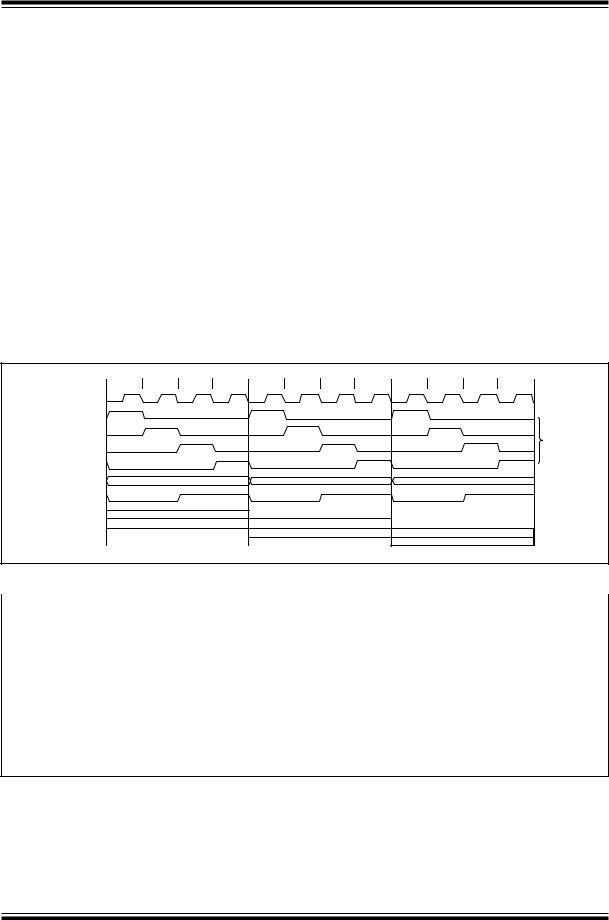
PIC16C7X
3.1Clocking Scheme/Instruction Cycle
The clock input (from OSC1) is internally divided by four to generate four non-overlapping quadrature clocks namely Q1, Q2, Q3 and Q4. Internally, the program counter (PC) is incremented every Q1, the instruction is fetched from the program memory and latched into the instruction register in Q4. The instruction is decoded and executed during the following Q1 through Q4. The clocks and instruction execution flow is shown in Figure 3-4.
3.2Instruction Flow/Pipelining
An “Instruction Cycle” consists of four Q cycles (Q1, Q2, Q3 and Q4). The instruction fetch and execute are pipelined such that fetch takes one instruction cycle while decode and execute takes another instruction cycle. However, due to the pipelining, each instruction effectively executes in one cycle. If an instruction causes the program counter to change (e.g. GOTO) then two cycles are required to complete the instruction (Example 3-1).
A fetch cycle begins with the program counter (PC) incrementing in Q1.
In the execution cycle, the fetched instruction is latched into the “Instruction Register" (IR) in cycle Q1. This instruction is then decoded and executed during the Q2, Q3, and Q4 cycles. Data memory is read during Q2 (operand read) and written during Q4 (destination write).
FIGURE 3-4: CLOCK/INSTRUCTION CYCLE
Q1 |
Q2 |
Q3 |
Q4 |
Q1 |
Q2 |
Q3 |
Q4 |
Q1 |
Q2 |
Q3 |
Q4 |
OSC1 |
|
|
|
|
|
|
|
|
|
|
|
Q1 |
|
|
|
|
|
|
|
|
|
|
|
Q2 |
|
|
|
|
|
|
|
|
|
|
Internal |
Q3 |
|
|
|
|
|
|
|
|
|
|
phase |
|
|
|
|
|
|
|
|
|
|
clock |
|
Q4 |
|
|
|
|
|
|
|
|
|
|
|
PC |
|
PC |
|
|
PC+1 |
|
|
|
|
PC+2 |
|
OSC2/CLKOUT |
|
|
|
|
|
|
|
|
|
|
|
(RC mode) |
Fetch INST (PC) |
|
|
|
|
|
|
|
|
|
|
|
|
|
|
|
|
|
|
|
|
||
|
Execute INST (PC-1) |
|
|
Fetch INST (PC+1) |
|
|
|
|
|
||
|
|
|
|
|
Execute INST (PC) |
|
|
Fetch INST (PC+2) |
|
||
|
|
|
|
|
|
|
|
|
Execute INST (PC+1) |
|
|
EXAMPLE 3-1: |
INSTRUCTION PIPELINE FLOW |
|
|
|
|
|
|
|
|||||||
|
|
|
|
Tcy0 |
|
Tcy1 |
|
Tcy2 |
|
Tcy3 |
|
Tcy4 |
|
Tcy5 |
|
|
|
|
|
|
|
|
|
|
|
||||||
|
|
|
|
|
|
|
|
|
|
|
|
|
|
|
|
1. |
MOVLW |
55h |
|
Fetch 1 |
|
Execute 1 |
|
|
|
|
|
|
|
|
|
|
|
|
|
|
|
|
|
|
|
|
|
|
|
|
|
2. |
MOVWF |
PORTB |
|
|
|
Fetch 2 |
|
Execute 2 |
|
|
|
|
|
|
|
|
|
|
|
|
|
|
|
|
|
|
|
|
|
|
|
3. |
CALL |
SUB_1 |
|
|
|
|
|
Fetch 3 |
|
Execute 3 |
|
|
|
|
|
|
|
|
|
|
|
|
|
|
|
|
|
|
|
|
|
4. |
BSF |
PORTA, BIT3 (Forced NOP) |
|
|
|
|
|
Fetch 4 |
|
Flush |
|
|
|
||
5. |
Instruction @ address SUB_1 |
|
|
|
|
|
|
|
Fetch SUB_1 |
|
Execute SUB_1 |
|
|||
|
|
|
|
|
|
|
|
|
|
|
|
|
|
|
|
All instructions are single cycle, except for any program branches. These take two cycles since the fetch instruction is “flushed” from the pipeline while the new instruction is being fetched and then executed.
1997 Microchip Technology Inc. |
DS30390E-page 17 |

PIC16C7X
NOTES:
DS30390E-page 18 |
1997 Microchip Technology Inc. |
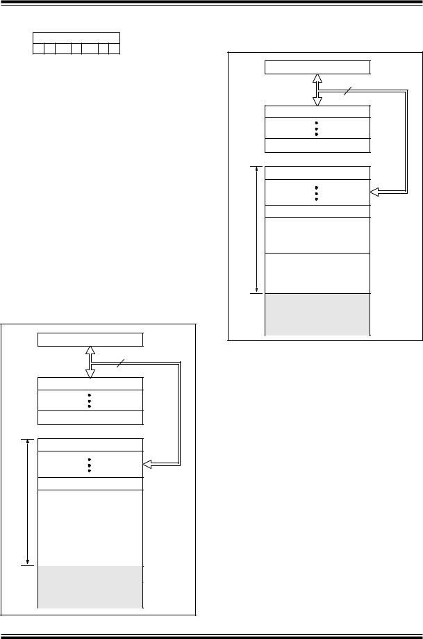
PIC16C7X
4.0MEMORY ORGANIZATION
Applicable Devices
72 73 73A 74 74A 76 77
4.1Program Memory Organization
The PIC16C7X family has a 13-bit program counter capable of addressing an 8K x 14 program memory space. The amount of program memory available to each device is listed below:
Device |
Program |
Address Range |
|
Memory |
|||
|
|
||
|
|
|
|
|
|
|
|
PIC16C72 |
2K x 14 |
0000h-07FFh |
|
PIC16C73 |
4K x 14 |
0000h-0FFFh |
|
PIC16C73A |
4K x 14 |
0000h-0FFFh |
|
PIC16C74 |
4K x 14 |
0000h-0FFFh |
|
PIC16C74A |
4K x 14 |
0000h-0FFFh |
|
PIC16C76 |
8K x 14 |
0000h-1FFFh |
|
PIC16C77 |
8K x 14 |
0000h-1FFFh |
|
|
|
|
For those devices with less than 8K program memory, accessing a location above the physically implemented address will cause a wraparound.
The reset vector is at 0000h and the interrupt vector is at 0004h.
FIGURE 4-1: PIC16C72 PROGRAM MEMORY MAP AND STACK
|
|
PC<12:0> |
|
|
CALL, RETURN |
13 |
|
|
RETFIE, RETLW |
|
|
|
|
|
|
|
Stack Level 1 |
|
|
|
Stack Level 8 |
|
|
|
Reset Vector |
0000h |
|
User Memory |
Interrupt Vector |
0004h |
|
|
|
0005h |
|
On-chip Program |
|
||
Space |
Memory |
|
|
|
|
|
|
|
|
|
07FFh |
|
|
|
0800h |
|
|
|
1FFFh |
FIGURE 4-2: PIC16C73/73A/74/74A PROGRAM MEMORY MAP AND STACK
|
|
|
PC<12:0> |
|
|
|
CALL, RETURN |
13 |
|
||
|
RETFIE, RETLW |
|
|||
|
|
|
|||
|
|
Stack Level 1 |
|
||
|
|
Stack Level 8 |
|
||
|
|
Reset Vector |
0000h |
||
User Memory |
|
Interrupt Vector |
0004h |
||
Space |
On-chip Program |
0005h |
|||
|
|||||
Memory (Page 0) |
07FFh |
||||
|
|
||||
On-chip Program |
0800h |
||||
|
|
||||
|
|
Memory (Page 1) |
|
||
|
|
|
|
0FFFh |
|
|
|
|
|
1000h |
|
|
|
|
|
1FFFh |
|
1997 Microchip Technology Inc. |
DS30390E-page 19 |
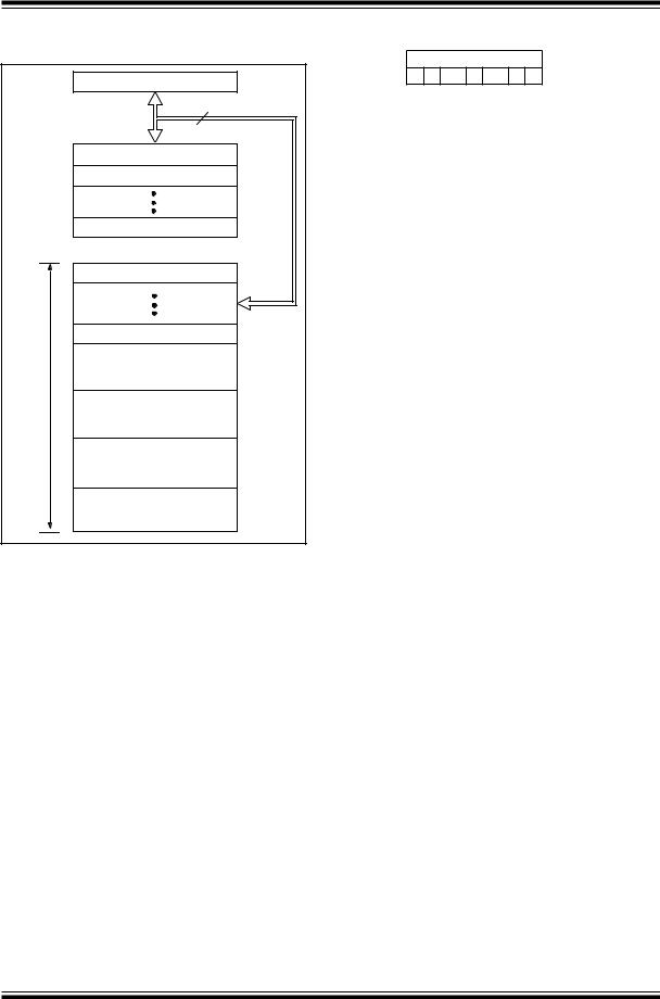
PIC16C7X
FIGURE 4-3: PIC16C76/77 PROGRAM MEMORY MAP AND STACK
|
|
PC<12:0> |
|
||
|
CALL, RETURN |
13 |
|
||
|
RETFIE, RETLW |
|
|
||
|
|
Stack Level 1 |
|
||
|
|
Stack Level 2 |
|
||
|
|
Stack Level 8 |
|
||
|
|
Reset Vector |
0000h |
||
|
|
Interrupt Vector |
0004h |
||
|
|
|
|
0005h |
|
User Memory |
|
On-Chip |
Page 0 |
|
|
Space |
|
|
07FFh |
||
On-Chip |
Page 1 |
0800h |
|||
0FFFh |
|||||
|
|
||||
|
|
1000h |
|||
|
|
On-Chip |
Page 2 |
||
|
|
|
|||
|
|
|
|
17FFh |
|
|
|
On-Chip |
Page 3 |
1800h |
|
|
|
|
|||
|
|
|
|
1FFFh |
|
4.2Data Memory Organization
Applicable Devices
72 73 73A 74 74A 76 77
The data memory is partitioned into multiple banks which contain the General Purpose Registers and the Special Function Registers. Bits RP1 and RP0 are the bank select bits.
RP1:RP0 (STATUS<6:5>)
=00 → Bank0
=01 → Bank1
=10 → Bank2
=11 → Bank3
Each bank extends up to 7Fh (128 bytes). The lower locations of each bank are reserved for the Special Function Registers. Above the Special Function Registers are General Purpose Registers, implemented as static RAM. All implemented banks contain special function registers. Some “high use” special function registers from one bank may be mirrored in another bank for code reduction and quicker access.
4.2.1GENERAL PURPOSE REGISTER FILE
The register file can be accessed either directly, or indirectly through the File Select Register FSR (Section 4.5).
DS30390E-page 20 |
1997 Microchip Technology Inc. |
PIC16C7X
FIGURE 4-4: PIC16C72 REGISTER FILE MAP
File |
|
|
|
|
File |
|||
Address |
|
|
|
Address |
||||
00h |
|
INDF(1) |
INDF(1) |
|
80h |
|||
01h |
|
TMR0 |
OPTION |
|
81h |
|||
02h |
|
PCL |
PCL |
|
82h |
|||
03h |
STATUS |
STATUS |
|
83h |
||||
|
|
|
|
|
|
|
|
84h |
04h |
|
FSR |
FSR |
|
||||
05h |
|
PORTA |
TRISA |
|
85h |
|||
06h |
|
PORTB |
TRISB |
|
86h |
|||
07h |
|
PORTC |
TRISC |
|
87h |
|||
08h |
|
|
|
|
|
88h |
||
|
|
|
|
|
|
|
89h |
|
09h |
|
|
|
|
|
|
||
0Ah |
|
PCLATH |
PCLATH |
|
8Ah |
|||
0Bh |
|
INTCON |
INTCON |
|
8Bh |
|||
0Ch |
|
PIR1 |
PIE1 |
|
8Ch |
|||
0Dh |
|
|
|
|
|
|
8Dh |
|
0Eh |
|
TMR1L |
PCON |
|
8Eh |
|||
|
|
|
|
|
|
|
|
8Fh |
0Fh |
|
TMR1H |
|
|
||||
10h |
|
T1CON |
|
|
90h |
|||
11h |
|
TMR2 |
|
|
91h |
|||
12h |
|
T2CON |
PR2 |
|
92h |
|||
|
|
|
|
|
|
|
|
93h |
13h |
SSPBUF |
SSPADD |
|
|||||
|
|
|
|
|
|
|
|
94h |
14h |
|
SSPCON |
SSPSTAT |
|
||||
15h |
|
CCPR1L |
|
|
95h |
|||
16h |
|
CCPR1H |
|
|
96h |
|||
17h |
|
CCP1CON |
|
|
97h |
|||
18h |
|
|
|
|
|
|
98h |
|
19h |
|
|
|
|
|
|
99h |
|
1Ah |
|
|
|
|
|
|
9Ah |
|
1Bh |
|
|
|
|
|
|
9Bh |
|
1Ch |
|
|
|
|
|
|
9Ch |
|
1Dh |
|
|
|
|
|
|
9Dh |
|
1Eh |
|
ADRES |
|
|
9Eh |
|||
1Fh |
|
ADCON0 |
ADCON1 |
|
9Fh |
|||
|
|
|
|
|
|
|
|
|
20h |
|
|
General |
General |
|
A0h |
||
|
|
|
|
|
|
|||
|
|
|
|
Purpose |
Purpose |
|
|
|
|
|
|
|
Register |
Register |
|
BFh |
|
|
|
|
|
|
|
|
|
|
|
|
|
|
|
|
|
|
C0h |
|
|
|
|
|
|
|
|
|
|
|
|
|
|
|
|
|
|
|
|
|
|
|
|
|
|
|
|
|
|
|
|
|
|
|
|
7Fh |
|
|
FFh |
|
Bank 0 |
Bank 1 |
|

 Unimplemented data memory locations, read as '0'.
Note 1: Not a physical register.
FIGURE 4-5: PIC16C73/73A/74/74A REGISTER FILE MAP
File |
|
|
|
File |
|
Address |
|
|
Address |
||
00h |
|
INDF(1) |
INDF(1) |
|
80h |
01h |
|
TMR0 |
OPTION |
|
81h |
02h |
|
PCL |
PCL |
|
82h |
03h |
|
|
|
|
83h |
|
STATUS |
STATUS |
|
||
04h |
|
|
|
|
84h |
|
FSR |
FSR |
|
||
05h |
|
PORTA |
TRISA |
|
85h |
06h |
|
PORTB |
TRISB |
|
86h |
07h |
|
PORTC |
TRISC |
|
87h |
08h |
|
PORTD(2) |
TRISD(2) |
|
88h |
09h |
|
PORTE(2) |
TRISE(2) |
|
89h |
0Ah |
|
PCLATH |
PCLATH |
|
8Ah |
0Bh |
|
INTCON |
INTCON |
|
8Bh |
0Ch |
|
PIR1 |
PIE1 |
|
8Ch |
0Dh |
|
PIR2 |
PIE2 |
|
8Dh |
0Eh |
|
|
|
|
8Eh |
|
TMR1L |
PCON |
|
||
0Fh |
|
|
|
|
8Fh |
|
TMR1H |
|
|
||
10h |
|
T1CON |
|
|
90h |
11h |
|
TMR2 |
|
|
91h |
12h |
|
T2CON |
PR2 |
|
92h |
13h |
|
|
|
|
93h |
|
SSPBUF |
SSPADD |
|
||
14h |
|
SSPCON |
SSPSTAT |
|
94h |
15h |
|
|
|
|
95h |
|
CCPR1L |
|
|
||
16h |
|
CCPR1H |
|
|
96h |
17h |
|
CCP1CON |
|
|
97h |
18h |
|
RCSTA |
TXSTA |
|
98h |
19h |
|
TXREG |
SPBRG |
|
99h |
1Ah |
|
|
|
|
9Ah |
|
RCREG |
|
|
||
1Bh |
|
CCPR2L |
|
|
9Bh |
1Ch |
|
CCPR2H |
|
|
9Ch |
1Dh |
|
CCP2CON |
|
|
9Dh |
1Eh |
|
ADRES |
|
|
9Eh |
1Fh |
|
ADCON0 |
ADCON1 |
|
9Fh |
20h |
|
|
|
|
A0h |
|
General |
General |
|
||
|
|
|
|
||
|
|
Purpose |
Purpose |
|
|
|
|
Register |
Register |
|
|
7Fh |
|
|
|
|
FFh |
|
|
Bank 0 |
Bank 1 |
|
|

 Unimplemented data memory locations, read as '0'.
Note 1: Not a physical register.
2:These registers are not physically implemented on the PIC16C73/73A, read as '0'.
1997 Microchip Technology Inc. |
DS30390E-page 21 |

PIC16C7X
FIGURE 4-6: PIC16C76/77 REGISTER FILE MAP
Indirect addr.(*) |
00h |
|
TMR0 |
01h |
|
PCL |
02h |
|
|
03h |
|
STATUS |
||
FSR |
04h |
|
PORTA |
05h |
|
PORTB |
06h |
|
PORTC |
07h |
|
PORTD (1) |
08h |
|
PORTE (1) |
09h |
|
PCLATH |
0Ah |
|
INTCON |
0Bh |
|
PIR1 |
0Ch |
|
PIR2 |
0Dh |
|
|
0Eh |
|
TMR1L |
||
|
0Fh |
|
TMR1H |
||
|
10h |
|
T1CON |
||
|
11h |
|
TMR2 |
||
|
12h |
|
T2CON |
||
|
13h |
|
SSPBUF |
||
SSPCON |
14h |
|
|
15h |
|
CCPR1L |
||
|
16h |
|
CCPR1H |
||
|
17h |
|
CCP1CON |
||
RCSTA |
18h |
|
TXREG |
19h |
|
RCREG |
1Ah |
|
CCPR2L |
1Bh |
|
CCPR2H |
1Ch |
|
CCP2CON |
1Dh |
|
ADRES |
1Eh |
|
ADCON0 |
1Fh |
|
|
20h |
|
General |
||
|
||
Purpose |
|
|
Register |
|
|
96 Bytes |
|
|
|
7Fh |
|
Bank 0 |
||
|
Indirect addr.(*) |
80h |
|
OPTION |
81h |
|
PCL |
82h |
|
STATUS |
83h |
|
FSR |
84h |
|
TRISA |
85h |
|
TRISB |
86h |
|
TRISC |
87h |
|
TRISD (1) |
88h |
|
TRISE (1) |
89h |
|
PCLATH |
8Ah |
|
INTCON |
8Bh |
|
PIE1 |
8Ch |
|
PIE2 |
8Dh |
|
PCON |
8Eh |
|
|
8Fh |
|
|
90h |
|
|
91h |
|
PR2 |
92h |
|
SSPADD |
93h |
|
SSPSTAT |
94h |
|
|
95h |
|
|
96h |
|
|
97h |
|
TXSTA |
98h |
|
SPBRG |
99h |
|
|
9Ah |
|
|
9Bh |
|
|
9Ch |
|
|
9Dh |
|
|
9Eh |
|
ADCON1 |
9Fh |
|
|
A0h |
|
General |
|
|
Purpose |
|
|
Register |
|
|
80 Bytes |
EFh |
|
|
||
accesses |
F0h |
|
|
||
70h-7Fh |
FFh |
|
|
||
Bank 1 |
||
|
Indirect addr.(*) |
100h |
|
TMR0 |
101h |
|
PCL |
102h |
|
|
103h |
|
STATUS |
||
FSR |
104h |
|
|
105h |
|
PORTB |
106h |
|
|
107h |
|
|
108h |
|
|
109h |
|
PCLATH |
10Ah |
|
INTCON |
10Bh |
|
|
10Ch |
|
|
10Dh |
|
|
10Eh |
|
|
10Fh |
|
|
110h |
|
|
111h |
|
|
112h |
|
|
113h |
|
|
114h |
|
|
115h |
|
|
116h |
|
General |
117h |
|
Purpose |
118h |
|
Register |
||
119h |
||
16 Bytes |
||
|
11Ah |
|
|
11Bh |
|
|
11Ch |
|
|
11Dh |
|
|
11Eh |
|
|
11Fh |
|
|
120h |
|
General |
||
|
||
Purpose |
|
|
Register |
|
|
80 Bytes |
16Fh |
|
|
||
accesses |
170h |
|
|
||
70h-7Fh |
17Fh |
|
|
||
Bank 2 |
|

 Unimplemented data memory locations, read as '0'. * Not a physical register.
|
File |
|
|
Address |
|
|
|
|
Indirect addr.(*) |
180h |
|
OPTION |
181h |
|
PCL |
182h |
|
STATUS |
183h |
|
FSR |
184h |
|
|
185h |
|
TRISB |
186h |
|
|
187h |
|
|
188h |
|
|
189h |
|
PCLATH |
18Ah |
|
INTCON |
18Bh |
|
|
18Ch |
|
|
18Dh |
|
|
18Eh |
|
|
18Fh |
|
|
190h |
|
|
191h |
|
|
192h |
|
|
193h |
|
|
194h |
|
|
195h |
|
General |
196h |
|
197h |
||
Purpose |
||
198h |
||
Register |
||
16 Bytes |
199h |
|
|
19Ah |
|
|
19Bh |
|
|
19Ch |
|
|
19Dh |
|
|
19Eh |
|
|
19Fh |
|
|
1A0h |
|
|
||
General |
|
|
Purpose |
|
|
Register |
|
|
80 Bytes |
1EFh |
|
|
||
accesses |
1F0h |
|
|
||
70h - 7Fh |
|
|
|
1FFh |
|
Bank 3 |
||
|
Note 1: PORTD, PORTE, TRISD, and TRISE are unimplemented on the PIC16C76, read as '0'.
Note: The upper 16 bytes of data memory in banks 1, 2, and 3 are mapped in Bank 0. This may require relocation of data memory usage in the user application code if upgrading to the PIC16C76/77.
DS30390E-page 22 |
1997 Microchip Technology Inc. |

PIC16C7X
4.2.2SPECIAL FUNCTION REGISTERS
The Special Function Registers are registers used by the CPU and Peripheral Modules for controlling the desired operation of the device. These registers are implemented as static RAM.
The special function registers can be classified into two sets (core and peripheral). Those registers associated with the “core” functions are described in this section, and those related to the operation of the peripheral features are described in the section of that peripheral feature.
TABLE 4-1: |
PIC16C72 SPECIAL FUNCTION REGISTER SUMMARY |
|
|
|
|
|
|||||||||||||||
|
|
|
|
|
|
|
|
|
|
|
|
|
|
|
|
|
|
Value on: |
Value on all |
||
Address |
Name |
Bit 7 |
Bit 6 |
Bit 5 |
Bit 4 |
Bit 3 |
|
Bit 2 |
Bit 1 |
Bit 0 |
POR, |
other resets |
|||||||||
|
|
|
|
|
|
|
|
|
|
|
|
|
|
|
|
|
|
BOR |
(3) |
||
|
|
|
|
|
|
|
|
|
|
|
|
|
|
|
|
|
|
|
|
|
|
|
|
|
|
|
|
|
|
|
|
|
|
|
|
|
|
|
|
|
|
|
|
Bank 0 |
|
|
|
|
|
|
|
|
|
|
|
|
|
|
|
|
|
|
|
|
|
|
|
|
|
|
|
|
|
|
|
|
|
|
|
||||||||
00h(1) |
INDF |
Addressing this location uses contents of FSR to address data memory (not a physical register) |
0000 |
0000 |
0000 |
0000 |
|||||||||||||||
01h |
TMR0 |
Timer0 module’s register |
|
|
|
|
|
|
|
|
|
|
|
|
|
xxxx xxxx |
uuuu uuuu |
||||
|
|
|
|
|
|
|
|
|
|
|
|
|
|
|
|
|
|||||
02h(1) |
PCL |
Program Counter's (PC) Least Significant Byte |
|
|
|
|
|
|
|
|
|
|
0000 |
0000 |
0000 |
0000 |
|||||
03h(1) |
STATUS |
IRP(4) |
RP1(4) |
RP0 |
|
TO |
|
|
PD |
|
|
|
Z |
DC |
C |
0001 |
1xxx |
000q |
quuu |
||
04h(1) |
FSR |
Indirect data memory address pointer |
|
|
|
|
|
|
|
|
|
|
xxxx xxxx |
uuuu uuuu |
|||||||
05h |
PORTA |
— |
— |
PORTA Data Latch when written: PORTA pins when read |
|
--0x 0000 |
--0u 0000 |
||||||||||||||
06h |
PORTB |
PORTB Data Latch when written: PORTB pins when read |
|
|
|
|
|
|
|
xxxx xxxx |
uuuu uuuu |
||||||||||
|
|
|
|
|
|
|
|
|
|
|
|
||||||||||
07h |
PORTC |
PORTC Data Latch when written: PORTC pins when read |
|
|
|
|
|
|
|
xxxx xxxx |
uuuu uuuu |
||||||||||
|
|
|
|
|
|
|
|
|
|
|
|
|
|
|
|
|
|
|
|
|
|
08h |
— |
Unimplemented |
|
|
|
|
|
|
|
|
|
|
|
|
|
|
— |
|
— |
|
|
09h |
— |
Unimplemented |
|
|
|
|
|
|
|
|
|
|
|
|
|
|
— |
|
— |
|
|
0Ah(1,2) |
PCLATH |
— |
— |
— |
Write Buffer for the upper 5 bits of the Program Counter |
---0 0000 |
---0 0000 |
||||||||||||||
0Bh(1) |
INTCON |
GIE |
PEIE |
T0IE |
INTE |
RBIE |
|
T0IF |
INTF |
RBIF |
0000 |
000x |
0000 |
000u |
|||||||
0Ch |
PIR1 |
— |
ADIF |
— |
|
— |
SSPIF |
CCP1IF |
TMR2IF |
TMR1IF |
-0-- 0000 |
-0-- 0000 |
|||||||||
0Dh |
— |
Unimplemented |
|
|
|
|
|
|
|
|
|
|
|
|
|
|
— |
|
— |
|
|
0Eh |
TMR1L |
Holding register for the Least Significant Byte of the 16-bit TMR1 register |
|
|
xxxx xxxx |
uuuu uuuu |
|||||||||||||||
|
|
|
|
|
|
|
|||||||||||||||
0Fh |
TMR1H |
Holding register for the Most Significant Byte of the 16-bit TMR1 register |
|
|
xxxx xxxx |
uuuu uuuu |
|||||||||||||||
|
|
|
|
|
|
|
|
|
|
|
|
|
|
|
|
||||||
10h |
T1CON |
— |
— |
T1CKPS1 |
T1CKPS0 |
T1OSCEN |
|
|
|
|
|
TMR1CS |
TMR1ON |
--00 0000 |
--uu uuuu |
||||||
T1SYNC |
|||||||||||||||||||||
11h |
TMR2 |
Timer2 module’s register |
|
|
|
|
|
|
|
|
|
|
|
|
|
0000 0000 |
0000 0000 |
||||
|
|
|
|
|
|
|
|
|
|
|
|
|
|
||||||||
12h |
T2CON |
— |
TOUTPS3 |
TOUTPS2 |
TOUTPS1 |
TOUTPS0 |
TMR2ON |
T2CKPS1 |
T2CKPS0 |
-000 0000 |
-000 0000 |
||||||||||
13h |
SSPBUF |
Synchronous Serial Port Receive Buffer/Transmit Register |
|
|
|
|
|
|
|
xxxx xxxx |
uuuu uuuu |
||||||||||
|
|
|
|
|
|
|
|
|
|
|
|
|
|||||||||
14h |
SSPCON |
WCOL |
SSPOV |
SSPEN |
CKP |
SSPM3 |
|
SSPM2 |
SSPM1 |
SSPM0 |
0000 0000 |
0000 0000 |
|||||||||
|
|
|
|
|
|
|
|
|
|
|
|
|
|
|
|
|
|
||||
15h |
CCPR1L |
Capture/Compare/PWM Register (LSB) |
|
|
|
|
|
|
|
|
|
|
xxxx xxxx |
uuuu uuuu |
|||||||
|
|
|
|
|
|
|
|
|
|
|
|
|
|
|
|||||||
16h |
CCPR1H |
Capture/Compare/PWM Register (MSB) |
|
|
|
|
|
|
|
|
|
|
xxxx xxxx |
uuuu uuuu |
|||||||
|
|
|
|
|
|
|
|
|
|
|
|
|
|
||||||||
17h |
CCP1CON |
— |
— |
CCP1X |
CCP1Y |
CCP1M3 |
CCP1M2 |
CCP1M1 |
CCP1M0 |
--00 0000 |
--00 0000 |
||||||||||
18h |
— |
Unimplemented |
|
|
|
|
|
|
|
|
|
|
|
|
|
|
— |
|
— |
|
|
19h |
— |
Unimplemented |
|
|
|
|
|
|
|
|
|
|
|
|
|
|
— |
|
— |
|
|
1Ah |
— |
Unimplemented |
|
|
|
|
|
|
|
|
|
|
|
|
|
|
— |
|
— |
|
|
1Bh |
— |
Unimplemented |
|
|
|
|
|
|
|
|
|
|
|
|
|
|
— |
|
— |
|
|
1Ch |
— |
Unimplemented |
|
|
|
|
|
|
|
|
|
|
|
|
|
|
— |
|
— |
|
|
1Dh |
— |
Unimplemented |
|
|
|
|
|
|
|
|
|
|
|
|
|
|
— |
|
— |
|
|
1Eh |
ADRES |
A/D Result Register |
|
|
|
|
|
|
|
|
|
|
|
|
|
|
xxxx xxxx |
uuuu uuuu |
|||
|
|
|
|
|
|
|
|
|
|
|
|
|
|||||||||
1Fh |
ADCON0 |
ADCS1 |
ADCS0 |
CHS2 |
CHS1 |
CHS0 |
|
|
|
— |
ADON |
0000 00-0 |
0000 00-0 |
||||||||
GO/DONE |
|||||||||||||||||||||
|
|
|
|
|
|
|
|
|
|
|
|
|
|
|
|
|
|
|
|
|
|
Legend: x = unknown, u = unchanged, q = value depends on condition, - = unimplemented read as '0'. Shaded locations are unimplemented, read as ‘0’.
Note 1: These registers can be addressed from either bank.
2:The upper byte of the program counter is not directly accessible. PCLATH is a holding register for the PC<12:8> whose contents are transferred to the upper byte of the program counter.
3:Other (non power-up) resets include external reset through MCLR and Watchdog Timer Reset.
4:The IRP and RP1 bits are reserved on the PIC16C72, always maintain these bits clear.
1997 Microchip Technology Inc. |
DS30390E-page 23 |

PIC16C7X
TABLE 4-1: |
PIC16C72 SPECIAL FUNCTION REGISTER SUMMARY (Cont.’d) |
|
|
|
|
||||||||||||||||||||||
|
|
|
|
|
|
|
|
|
|
|
|
|
|
|
|
|
|
|
|
|
|
|
|
Value on: |
Value on all |
||
Address |
Name |
|
Bit 7 |
|
Bit 6 |
Bit 5 |
Bit 4 |
Bit 3 |
Bit 2 |
|
Bit 1 |
|
Bit 0 |
POR, |
other resets |
||||||||||||
|
|
|
|
|
|
|
|
|
|
|
|
|
|
|
|
|
|
|
|
|
|
|
|
BOR |
(3) |
||
|
|
|
|
|
|
|
|
|
|
|
|
|
|
|
|
|
|
|
|
|
|
|
|
|
|
|
|
|
|
|
|
|
|
|
|
|
|
|
|
|
|
|
|
|
|
|
|
|
|
|
|
|
|
|
|
Bank 1 |
|
|
|
|
|
|
|
|
|
|
|
|
|
|
|
|
|
|
|
|
|
|
|
|
|
|
|
|
|
|
|
|
|
|
|
|
|
|
|
||||||||||||||||
80h(1) |
INDF |
Addressing this location uses contents of FSR to address data memory (not a physical register) |
0000 |
0000 |
0000 |
0000 |
|||||||||||||||||||||
81h |
OPTION |
|
|
|
INTEDG |
T0CS |
T0SE |
PSA |
PS2 |
|
PS1 |
|
PS0 |
1111 |
1111 |
1111 1111 |
|||||||||||
|
RBPU |
||||||||||||||||||||||||||
|
|
|
|
|
|
|
|
|
|
|
|
|
|
|
|
|
|
|
|
|
|
||||||
82h(1) |
PCL |
Program Counter's (PC) Least Significant Byte |
|
|
|
|
|
|
|
|
|
|
|
|
0000 |
0000 |
0000 |
0000 |
|||||||||
83h(1) |
STATUS |
|
IRP(4) |
|
RP1(4) |
RP0 |
|
TO |
|
|
PD |
|
Z |
|
DC |
|
C |
0001 |
1xxx |
000q |
quuu |
||||||
84h(1) |
FSR |
Indirect data memory address pointer |
|
|
|
|
|
|
|
|
|
|
|
|
xxxx xxxx |
uuuu uuuu |
|||||||||||
85h |
TRISA |
|
— |
|
— |
PORTA Data Direction Register |
|
|
|
|
|
|
|
|
|
--11 1111 |
--11 1111 |
||||||||||
86h |
TRISB |
PORTB Data Direction Register |
|
|
|
|
|
|
|
|
|
|
|
|
|
|
|
1111 |
1111 |
1111 1111 |
|||||||
|
|
|
|
|
|
|
|
|
|
|
|
|
|
|
|
|
|
|
|
|
|||||||
87h |
TRISC |
PORTC Data Direction Register |
|
|
|
|
|
|
|
|
|
|
|
|
|
|
|
1111 |
1111 |
1111 1111 |
|||||||
|
|
|
|
|
|
|
|
|
|
|
|
|
|
|
|
|
|
|
|
|
|
|
|
||||
88h |
— |
Unimplemented |
|
|
|
|
|
|
|
|
|
|
|
|
|
|
|
|
|
|
— |
— |
|||||
89h |
— |
Unimplemented |
|
|
|
|
|
|
|
|
|
|
|
|
|
|
|
|
|
|
— |
— |
|||||
8Ah(1,2) |
PCLATH |
|
— |
|
— |
— |
Write Buffer for the upper 5 bits of the PC |
|
|
|
---0 0000 |
---0 0000 |
|||||||||||||||
8Bh(1) |
INTCON |
|
GIE |
|
PEIE |
T0IE |
INTE |
RBIE |
T0IF |
INTF |
RBIF |
0000 |
000x |
0000 000u |
|||||||||||||
8Ch |
PIE1 |
|
— |
|
ADIE |
— |
|
— |
SSPIE |
CCP1IE |
TMR2IE |
TMR1IE |
-0-- 0000 |
-0-- 0000 |
|||||||||||||
8Dh |
— |
Unimplemented |
|
|
|
|
|
|
|
|
|
|
|
|
|
|
|
|
|
|
— |
— |
|||||
8Eh |
PCON |
|
— |
|
— |
— |
|
— |
|
— |
— |
|
|
|
|
|
|
---- --uu |
|||||||||
|
|
|
|
POR |
BOR |
||||||||||||||||||||||
8Fh |
— |
Unimplemented |
|
|
|
|
|
|
|
|
|
|
|
|
|
|
|
|
|
|
— |
— |
|||||
90h |
— |
Unimplemented |
|
|
|
|
|
|
|
|
|
|
|
|
|
|
|
|
|
|
— |
— |
|||||
91h |
— |
Unimplemented |
|
|
|
|
|
|
|
|
|
|
|
|
|
|
|
|
|
|
— |
— |
|||||
92h |
PR2 |
Timer2 Period Register |
|
|
|
|
|
|
|
|
|
|
|
|
|
|
|
|
|
|
1111 |
1111 |
1111 1111 |
||||
|
|
|
|
|
|
|
|
|
|
|
|
|
|
|
|||||||||||||
93h |
SSPADD |
Synchronous Serial Port (I2C mode) Address Register |
|
|
|
|
|
|
|
|
|
0000 |
0000 |
0000 0000 |
|||||||||||||
94h |
SSPSTAT |
|
— |
|
— |
D/A |
|
|
|
P |
|
S |
|
|
|
|
UA |
|
BF |
--00 0000 |
--00 0000 |
||||||
|
|
|
|
|
R/W |
|
|
|
|||||||||||||||||||
95h |
— |
Unimplemented |
|
|
|
|
|
|
|
|
|
|
|
|
|
|
|
|
|
|
— |
— |
|||||
96h |
— |
Unimplemented |
|
|
|
|
|
|
|
|
|
|
|
|
|
|
|
|
|
|
— |
— |
|||||
97h |
— |
Unimplemented |
|
|
|
|
|
|
|
|
|
|
|
|
|
|
|
|
|
|
— |
— |
|||||
98h |
— |
Unimplemented |
|
|
|
|
|
|
|
|
|
|
|
|
|
|
|
|
|
|
— |
— |
|||||
99h |
— |
Unimplemented |
|
|
|
|
|
|
|
|
|
|
|
|
|
|
|
|
|
|
— |
— |
|||||
9Ah |
— |
Unimplemented |
|
|
|
|
|
|
|
|
|
|
|
|
|
|
|
|
|
|
— |
— |
|||||
9Bh |
— |
Unimplemented |
|
|
|
|
|
|
|
|
|
|
|
|
|
|
|
|
|
|
— |
— |
|||||
9Ch |
— |
Unimplemented |
|
|
|
|
|
|
|
|
|
|
|
|
|
|
|
|
|
|
— |
— |
|||||
9Dh |
— |
Unimplemented |
|
|
|
|
|
|
|
|
|
|
|
|
|
|
|
|
|
|
— |
— |
|||||
9Eh |
— |
Unimplemented |
|
|
|
|
|
|
|
|
|
|
|
|
|
|
|
|
|
|
— |
— |
|||||
9Fh |
ADCON1 |
|
— |
|
— |
— |
|
— |
|
— |
PCFG2 |
PCFG1 |
PCFG0 |
---- -000 |
---- -000 |
||||||||||||
|
|
|
|
|
|
|
|
|
|
|
|
|
|
|
|
|
|
|
|
|
|
|
|
|
|
|
|
Legend: x = unknown, u = unchanged, q = value depends on condition, - = unimplemented read as '0'. Shaded locations are unimplemented, read as ‘0’.
Note 1: These registers can be addressed from either bank.
2:The upper byte of the program counter is not directly accessible. PCLATH is a holding register for the PC<12:8> whose contents are transferred to the upper byte of the program counter.
3:Other (non power-up) resets include external reset through MCLR and Watchdog Timer Reset.
4:The IRP and RP1 bits are reserved on the PIC16C72, always maintain these bits clear.
DS30390E-page 24 |
1997 Microchip Technology Inc. |

PIC16C7X
TABLE 4-2: |
PIC16C73/73A/74/74A SPECIAL FUNCTION REGISTER SUMMARY |
|
|
|
|
|||||||||||||||||
|
|
|
|
|
|
|
|
|
|
|
|
|
|
|
|
|
|
|
Value on: |
Value on all |
||
Address |
Name |
|
Bit 7 |
Bit 6 |
Bit 5 |
Bit 4 |
Bit 3 |
|
Bit 2 |
Bit 1 |
Bit 0 |
POR, |
other resets |
|||||||||
|
|
|
|
|
|
|
|
|
|
|
|
|
|
|
|
|
|
|
BOR |
(2) |
||
|
|
|
|
|
|
|
|
|
|
|
|
|
|
|
|
|
|
|
|
|
|
|
|
|
|
|
|
|
|
|
|
|
|
|
|
|
|
|
|
|
|
|
|
|
|
Bank 0 |
|
|
|
|
|
|
|
|
|
|
|
|
|
|
|
|
|
|
|
|
|
|
|
|
|
|
|
|
|
|
|
|
|
|
|
|
|||||||||
00h(4) |
INDF |
|
Addressing this location uses contents of FSR to address data memory (not a physical register) |
0000 |
0000 |
0000 |
0000 |
|||||||||||||||
01h |
TMR0 |
|
Timer0 module’s register |
|
|
|
|
|
|
|
|
|
|
|
|
|
xxxx xxxx |
uuuu uuuu |
||||
|
|
|
|
|
|
|
|
|
|
|
|
|
|
|
|
|
|
|||||
02h(4) |
PCL |
|
Program Counter's (PC) Least Significant Byte |
|
|
|
|
|
|
|
|
|
|
0000 |
0000 |
0000 |
0000 |
|||||
03h(4) |
STATUS |
|
IRP(7) |
RP1(7) |
RP0 |
|
TO |
|
|
PD |
|
|
|
Z |
DC |
C |
0001 |
1xxx |
000q |
quuu |
||
04h(4) |
FSR |
|
Indirect data memory address pointer |
|
|
|
|
|
|
|
|
|
|
xxxx xxxx |
uuuu uuuu |
|||||||
05h |
PORTA |
|
— |
— |
PORTA Data Latch when written: PORTA pins when read |
|
--0x 0000 |
--0u 0000 |
||||||||||||||
06h |
PORTB |
|
PORTB Data Latch when written: PORTB pins when read |
|
|
|
|
|
|
|
xxxx xxxx |
uuuu uuuu |
||||||||||
|
|
|
|
|
|
|
|
|
|
|
|
|
||||||||||
07h |
PORTC |
|
PORTC Data Latch when written: PORTC pins when read |
|
|
|
|
|
|
|
xxxx xxxx |
uuuu uuuu |
||||||||||
|
|
|
|
|
|
|
|
|
|
|
|
|
||||||||||
08h(5) |
PORTD |
|
PORTD Data Latch when written: PORTD pins when read |
|
|
|
|
|
|
|
xxxx xxxx |
uuuu uuuu |
||||||||||
09h(5) |
PORTE |
|
— |
— |
— |
|
— |
|
— |
|
RE2 |
RE1 |
RE0 |
---- -xxx |
---- -uuu |
|||||||
0Ah(1,4) |
PCLATH |
|
— |
— |
— |
Write Buffer for the upper 5 bits of the Program Counter |
---0 0000 |
---0 0000 |
||||||||||||||
0Bh(4) |
INTCON |
|
GIE |
PEIE |
T0IE |
INTE |
RBIE |
|
T0IF |
INTF |
RBIF |
0000 |
000x |
0000 |
000u |
|||||||
0Ch |
PIR1 |
|
PSPIF(3) |
ADIF |
RCIF |
TXIF |
SSPIF |
|
CCP1IF |
TMR2IF |
TMR1IF |
0000 |
0000 |
0000 |
0000 |
|||||||
0Dh |
PIR2 |
|
— |
— |
— |
|
– |
|
— |
|
|
— |
— |
CCP2IF |
---- ---0 |
---- ---0 |
||||||
0Eh |
TMR1L |
|
Holding register for the Least Significant Byte of the 16-bit TMR1 register |
|
|
xxxx xxxx |
uuuu uuuu |
|||||||||||||||
|
|
|
|
|
|
|
|
|||||||||||||||
0Fh |
TMR1H |
|
Holding register for the Most Significant Byte of the 16-bit TMR1 register |
|
|
xxxx xxxx |
uuuu uuuu |
|||||||||||||||
|
|
|
|
|
|
|
|
|
|
|
|
|
|
|
|
|
||||||
10h |
T1CON |
|
— |
— |
T1CKPS1 |
T1CKPS0 |
T1OSCEN |
|
|
|
|
|
TMR1CS |
TMR1ON |
--00 0000 |
--uu uuuu |
||||||
|
T1SYNC |
|||||||||||||||||||||
11h |
TMR2 |
|
Timer2 module’s register |
|
|
|
|
|
|
|
|
|
|
|
|
|
0000 |
0000 |
0000 |
0000 |
||
|
|
|
|
|
|
|
|
|
|
|
|
|
|
|
||||||||
12h |
T2CON |
|
— |
TOUTPS3 |
TOUTPS2 |
TOUTPS1 |
TOUTPS0 |
TMR2ON |
T2CKPS1 |
T2CKPS0 |
-000 0000 |
-000 0000 |
||||||||||
13h |
SSPBUF |
|
Synchronous Serial Port Receive Buffer/Transmit Register |
|
|
|
|
|
|
|
xxxx xxxx |
uuuu uuuu |
||||||||||
|
|
|
|
|
|
|
|
|
|
|
|
|
|
|
|
|||||||
14h |
SSPCON |
|
WCOL |
SSPOV |
SSPEN |
CKP |
SSPM3 |
|
SSPM2 |
SSPM1 |
SSPM0 |
0000 |
0000 |
0000 |
0000 |
|||||||
|
|
|
|
|
|
|
|
|
|
|
|
|
|
|
|
|
|
|
||||
15h |
CCPR1L |
|
Capture/Compare/PWM Register1 (LSB) |
|
|
|
|
|
|
|
|
|
|
xxxx xxxx |
uuuu uuuu |
|||||||
|
|
|
|
|
|
|
|
|
|
|
|
|
|
|
|
|||||||
16h |
CCPR1H |
|
Capture/Compare/PWM Register1 (MSB) |
|
|
|
|
|
|
|
|
|
|
xxxx xxxx |
uuuu uuuu |
|||||||
|
|
|
|
|
|
|
|
|
|
|
|
|
|
|
||||||||
17h |
CCP1CON |
|
— |
— |
CCP1X |
CCP1Y |
CCP1M3 |
CCP1M2 |
CCP1M1 |
CCP1M0 |
--00 0000 |
--00 0000 |
||||||||||
18h |
RCSTA |
|
SPEN |
RX9 |
SREN |
CREN |
|
— |
|
FERR |
OERR |
RX9D |
0000 |
-00x |
0000 |
-00x |
||||||
19h |
TXREG |
|
USART Transmit Data Register |
|
|
|
|
|
|
|
|
|
|
|
|
|
0000 |
0000 |
0000 |
0000 |
||
|
|
|
|
|
|
|
|
|
|
|
|
|
|
|
|
|
|
|
|
|
||
1Ah |
RCREG |
|
USART Receive Data Register |
|
|
|
|
|
|
|
|
|
|
|
|
|
0000 |
0000 |
0000 |
0000 |
||
|
|
|
|
|
|
|
|
|
|
|
|
|
|
|
|
|||||||
1Bh |
CCPR2L |
|
Capture/Compare/PWM Register2 (LSB) |
|
|
|
|
|
|
|
|
|
|
xxxx xxxx |
uuuu uuuu |
|||||||
|
|
|
|
|
|
|
|
|
|
|
|
|
|
|
|
|||||||
1Ch |
CCPR2H |
|
Capture/Compare/PWM Register2 (MSB) |
|
|
|
|
|
|
|
|
|
|
xxxx xxxx |
uuuu uuuu |
|||||||
|
|
|
|
|
|
|
|
|
|
|
|
|
|
|
||||||||
1Dh |
CCP2CON |
|
— |
— |
CCP2X |
CCP2Y |
CCP2M3 |
CCP2M2 |
CCP2M1 |
CCP2M0 |
--00 0000 |
--00 0000 |
||||||||||
1Eh |
ADRES |
|
A/D Result Register |
|
|
|
|
|
|
|
|
|
|
|
|
|
|
xxxx xxxx |
uuuu uuuu |
|||
|
|
|
|
|
|
|
|
|
|
|
|
|
|
|
|
|||||||
1Fh |
ADCON0 |
|
ADCS1 |
ADCS0 |
CHS2 |
CHS1 |
CHS0 |
|
|
|
— |
ADON |
0000 |
00-0 |
0000 |
00-0 |
||||||
|
GO/DONE |
|||||||||||||||||||||
|
|
|
|
|
|
|
|
|
|
|
|
|
|
|
|
|
|
|
|
|
|
|
Legend: x = unknown, u = unchanged, q = value depends on condition, - = unimplemented read as '0'. Shaded locations are unimplemented, read as ‘0’.
Note 1: The upper byte of the program counter is not directly accessible. PCLATH is a holding register for the PC<12:8> whose contents are transferred to the upper byte of the program counter.
2:Other (non power-up) resets include external reset through MCLR and Watchdog Timer Reset.
3:Bits PSPIE and PSPIF are reserved on the PIC16C73/73A, always maintain these bits clear.
4:These registers can be addressed from either bank.
5:PORTD and PORTE are not physically implemented on the PIC16C73/73A, read as ‘0’.
6:Brown-out Reset is not implemented on the PIC16C73 or the PIC16C74, read as '0'.
7:The IRP and RP1 bits are reserved on the PIC16C73/73A/74/74A, always maintain these bits clear.
1997 Microchip Technology Inc. |
DS30390E-page 25 |

PIC16C7X
TABLE 4-2: |
PIC16C73/73A/74/74A SPECIAL FUNCTION REGISTER SUMMARY |
(Cont.’d) |
|
|
|||||||||||||||||||||||||
|
|
|
|
|
|
|
|
|
|
|
|
|
|
|
|
|
|
|
|
|
|
|
|
|
|
Value on: |
Value on all |
||
Address |
Name |
|
|
Bit 7 |
Bit 6 |
Bit 5 |
Bit 4 |
|
Bit 3 |
Bit 2 |
|
Bit 1 |
|
Bit 0 |
POR, |
other resets |
|||||||||||||
|
|
|
|
|
|
|
|
|
|
|
|
|
|
|
|
|
|
|
|
|
|
|
|
|
|
BOR |
(2) |
||
|
|
|
|
|
|
|
|
|
|
|
|
|
|
|
|
|
|
|
|
|
|
|
|
|
|
|
|
|
|
|
|
|
|
|
|
|
|
|
|
|
|
|
|
|
|
|
|
|
|
|
|
|
|
|
|
|
|
|
|
Bank 1 |
|
|
|
|
|
|
|
|
|
|
|
|
|
|
|
|
|
|
|
|
|
|
|
|
|
|
|
|
|
|
|
|
|
|
|
|
|
|
|
|
|
|
|||||||||||||||||
80h(4) |
INDF |
|
Addressing this location uses contents of FSR to address data memory (not a physical register) |
0000 |
0000 |
0000 |
0000 |
||||||||||||||||||||||
81h |
OPTION |
|
|
|
|
INTEDG |
T0CS |
T0SE |
|
PSA |
PS2 |
|
PS1 |
|
PS0 |
1111 |
1111 |
1111 |
1111 |
||||||||||
|
|
RBPU |
|||||||||||||||||||||||||||
|
|
|
|
|
|
|
|
|
|
|
|
|
|
|
|
|
|
|
|
|
|
|
|
||||||
82h(4) |
PCL |
|
Program Counter's (PC) Least Significant Byte |
|
|
|
|
|
|
|
|
|
|
|
|
0000 |
0000 |
0000 |
0000 |
||||||||||
83h(4) |
STATUS |
|
|
IRP(7) |
RP1(7) |
RP0 |
|
TO |
|
|
|
PD |
|
Z |
|
DC |
|
C |
0001 |
1xxx |
000q |
quuu |
|||||||
84h(4) |
FSR |
|
Indirect data memory address pointer |
|
|
|
|
|
|
|
|
|
|
|
|
xxxx xxxx |
uuuu uuuu |
||||||||||||
85h |
TRISA |
|
|
— |
— |
PORTA Data Direction Register |
|
|
|
|
|
|
|
|
|
--11 1111 |
--11 1111 |
||||||||||||
86h |
TRISB |
|
PORTB Data Direction Register |
|
|
|
|
|
|
|
|
|
|
|
|
|
|
|
|
1111 |
1111 |
1111 |
1111 |
||||||
|
|
|
|
|
|
|
|
|
|
|
|
|
|
|
|
|
|
|
|
|
|
|
|
||||||
87h |
TRISC |
|
PORTC Data Direction Register |
|
|
|
|
|
|
|
|
|
|
|
|
|
|
|
|
1111 |
1111 |
1111 |
1111 |
||||||
|
|
|
|
|
|
|
|
|
|
|
|
|
|
|
|
|
|
|
|
|
|
|
|
||||||
88h(5) |
TRISD |
|
PORTD Data Direction Register |
|
|
|
|
|
|
|
|
|
|
|
|
|
|
|
|
1111 |
1111 |
1111 |
1111 |
||||||
89h(5) |
TRISE |
|
|
IBF |
OBF |
IBOV |
PSPMODE |
|
|
— |
PORTE Data Direction Bits |
0000 |
-111 |
0000 |
-111 |
||||||||||||||
8Ah(1,4) |
PCLATH |
|
|
— |
— |
— |
Write Buffer for the upper 5 bits of the Program Counter |
---0 0000 |
---0 0000 |
||||||||||||||||||||
8Bh(4) |
INTCON |
|
|
GIE |
PEIE |
T0IE |
INTE |
|
RBIE |
T0IF |
INTF |
|
RBIF |
0000 |
000x |
0000 |
000u |
||||||||||||
8Ch |
PIE1 |
|
PSPIE(3) |
ADIE |
RCIE |
TXIE |
|
SSPIE |
CCP1IE |
TMR2IE |
TMR1IE |
0000 |
0000 |
0000 |
0000 |
||||||||||||||
8Dh |
PIE2 |
|
|
— |
— |
— |
|
— |
|
|
— |
— |
|
— |
CCP2IE |
---- ---0 |
---- ---0 |
||||||||||||
8Eh |
PCON |
|
|
— |
— |
— |
|
— |
|
|
— |
— |
|
|
|
|
|
(6) |
---- --uu |
||||||||||
|
|
|
|
|
POR |
BOR |
|||||||||||||||||||||||
8Fh |
— |
|
Unimplemented |
|
|
|
|
|
|
|
|
|
|
|
|
|
|
|
|
|
|
|
— |
— |
|||||
90h |
— |
|
Unimplemented |
|
|
|
|
|
|
|
|
|
|
|
|
|
|
|
|
|
|
|
— |
— |
|||||
91h |
— |
|
Unimplemented |
|
|
|
|
|
|
|
|
|
|
|
|
|
|
|
|
|
|
|
— |
— |
|||||
92h |
PR2 |
|
Timer2 Period Register |
|
|
|
|
|
|
|
|
|
|
|
|
|
|
|
|
|
|
|
1111 |
1111 |
1111 |
1111 |
|||
|
|
|
|
|
|
|
|
|
|
|
|
|
|
|
|
|
|
|
|
||||||||||
93h |
SSPADD |
|
Synchronous Serial Port (I2C mode) Address Register |
|
|
|
|
|
|
|
|
|
|
|
|
0000 |
0000 |
0000 |
0000 |
||||||||||
94h |
SSPSTAT |
|
|
— |
— |
D/A |
|
|
|
P |
|
|
S |
|
|
|
|
UA |
|
BF |
--00 0000 |
--00 0000 |
|||||||
|
|
|
|
|
R/W |
|
|
|
|||||||||||||||||||||
95h |
— |
|
Unimplemented |
|
|
|
|
|
|
|
|
|
|
|
|
|
|
|
|
|
|
|
— |
— |
|||||
96h |
— |
|
Unimplemented |
|
|
|
|
|
|
|
|
|
|
|
|
|
|
|
|
|
|
|
— |
— |
|||||
97h |
— |
|
Unimplemented |
|
|
|
|
|
|
|
|
|
|
|
|
|
|
|
|
|
|
|
— |
— |
|||||
98h |
TXSTA |
|
CSRC |
TX9 |
TXEN |
SYNC |
|
|
— |
BRGH |
TRMT |
TX9D |
0000 |
-010 |
0000 |
-010 |
|||||||||||||
99h |
SPBRG |
|
Baud Rate Generator Register |
|
|
|
|
|
|
|
|
|
|
|
|
|
|
|
|
0000 |
0000 |
0000 |
0000 |
||||||
|
|
|
|
|
|
|
|
|
|
|
|
|
|
|
|
|
|
|
|
|
|
|
|
|
|
||||
9Ah |
— |
|
Unimplemented |
|
|
|
|
|
|
|
|
|
|
|
|
|
|
|
|
|
|
|
— |
— |
|||||
9Bh |
— |
|
Unimplemented |
|
|
|
|
|
|
|
|
|
|
|
|
|
|
|
|
|
|
|
— |
— |
|||||
9Ch |
— |
|
Unimplemented |
|
|
|
|
|
|
|
|
|
|
|
|
|
|
|
|
|
|
|
— |
— |
|||||
9Dh |
— |
|
Unimplemented |
|
|
|
|
|
|
|
|
|
|
|
|
|
|
|
|
|
|
|
— |
— |
|||||
9Eh |
— |
|
Unimplemented |
|
|
|
|
|
|
|
|
|
|
|
|
|
|
|
|
|
|
|
— |
— |
|||||
9Fh |
ADCON1 |
|
|
— |
— |
— |
|
— |
|
|
— |
PCFG2 |
PCFG1 |
PCFG0 |
---- -000 |
---- -000 |
|||||||||||||
|
|
|
|
|
|
|
|
|
|
|
|
|
|
|
|
|
|
|
|
|
|
|
|
|
|
|
|
|
|
Legend: x = unknown, u = unchanged, q = value depends on condition, - = unimplemented read as '0'. Shaded locations are unimplemented, read as ‘0’.
Note 1: The upper byte of the program counter is not directly accessible. PCLATH is a holding register for the PC<12:8> whose contents are transferred to the upper byte of the program counter.
2:Other (non power-up) resets include external reset through MCLR and Watchdog Timer Reset.
3:Bits PSPIE and PSPIF are reserved on the PIC16C73/73A, always maintain these bits clear.
4:These registers can be addressed from either bank.
5:PORTD and PORTE are not physically implemented on the PIC16C73/73A, read as ‘0’.
6:Brown-out Reset is not implemented on the PIC16C73 or the PIC16C74, read as '0'.
7:The IRP and RP1 bits are reserved on the PIC16C73/73A/74/74A, always maintain these bits clear.
DS30390E-page 26 |
1997 Microchip Technology Inc. |

PIC16C7X
TABLE 4-3: |
PIC16C76/77 SPECIAL FUNCTION REGISTER SUMMARY |
|
|
|
|
|
||||||||||||||||
|
|
|
|
|
|
|
|
|
|
|
|
|
|
|
|
|
|
|
Value on: |
Value on all |
||
Address |
Name |
|
Bit 7 |
Bit 6 |
Bit 5 |
Bit 4 |
Bit 3 |
|
Bit 2 |
Bit 1 |
Bit 0 |
POR, |
other resets |
|||||||||
|
|
|
|
|
|
|
|
|
|
|
|
|
|
|
|
|
|
|
BOR |
(2) |
||
|
|
|
|
|
|
|
|
|
|
|
|
|
|
|
|
|
|
|
|
|
|
|
|
|
|
|
|
|
|
|
|
|
|
|
|
|
|
|
|
|
|
|
|
|
|
Bank 0 |
|
|
|
|
|
|
|
|
|
|
|
|
|
|
|
|
|
|
|
|
|
|
|
|
|
|
|
|
|
|
|
|
|
|
|
||||||||||
00h(4) |
INDF |
|
Addressing this location uses contents of FSR to address data memory (not a physical register) |
0000 |
0000 |
0000 |
0000 |
|||||||||||||||
01h |
TMR0 |
|
Timer0 module’s register |
|
|
|
|
|
|
|
|
|
|
|
|
|
xxxx xxxx |
uuuu uuuu |
||||
|
|
|
|
|
|
|
|
|
|
|
|
|
|
|
|
|
|
|||||
02h(4) |
PCL |
|
Program Counter's (PC) Least Significant Byte |
|
|
|
|
|
|
|
|
|
|
0000 |
0000 |
0000 |
0000 |
|||||
03h(4) |
STATUS |
|
IRP |
RP1 |
RP0 |
|
TO |
|
|
PD |
|
|
|
Z |
DC |
C |
0001 |
1xxx |
000q |
quuu |
||
04h(4) |
FSR |
|
Indirect data memory address pointer |
|
|
|
|
|
|
|
|
|
|
xxxx xxxx |
uuuu uuuu |
|||||||
05h |
PORTA |
|
— |
— |
PORTA Data Latch when written: PORTA pins when read |
|
--0x 0000 |
--0u 0000 |
||||||||||||||
06h |
PORTB |
|
PORTB Data Latch when written: PORTB pins when read |
|
|
|
|
|
|
|
xxxx xxxx |
uuuu uuuu |
||||||||||
|
|
|
|
|
|
|
|
|
|
|
|
|
||||||||||
07h |
PORTC |
|
PORTC Data Latch when written: PORTC pins when read |
|
|
|
|
|
|
|
xxxx xxxx |
uuuu uuuu |
||||||||||
|
|
|
|
|
|
|
|
|
|
|
|
|
||||||||||
08h(5) |
PORTD |
|
PORTD Data Latch when written: PORTD pins when read |
|
|
|
|
|
|
|
xxxx xxxx |
uuuu uuuu |
||||||||||
09h(5) |
PORTE |
|
— |
— |
— |
|
— |
|
— |
|
RE2 |
RE1 |
RE0 |
---- -xxx |
---- -uuu |
|||||||
0Ah(1,4) |
PCLATH |
|
— |
— |
— |
Write Buffer for the upper 5 bits of the Program Counter |
---0 0000 |
---0 0000 |
||||||||||||||
0Bh(4) |
INTCON |
|
GIE |
PEIE |
T0IE |
INTE |
RBIE |
|
T0IF |
INTF |
RBIF |
0000 |
000x |
0000 |
000u |
|||||||
0Ch |
PIR1 |
|
PSPIF(3) |
ADIF |
RCIF |
TXIF |
SSPIF |
|
CCP1IF |
TMR2IF |
TMR1IF |
0000 |
0000 |
0000 |
0000 |
|||||||
0Dh |
PIR2 |
|
— |
— |
— |
|
– |
|
— |
|
|
— |
— |
CCP2IF |
---- ---0 |
---- ---0 |
||||||
0Eh |
TMR1L |
|
Holding register for the Least Significant Byte of the 16-bit TMR1 register |
|
|
xxxx xxxx |
uuuu uuuu |
|||||||||||||||
|
|
|
|
|
|
|
|
|||||||||||||||
0Fh |
TMR1H |
|
Holding register for the Most Significant Byte of the 16-bit TMR1 register |
|
|
xxxx xxxx |
uuuu uuuu |
|||||||||||||||
|
|
|
|
|
|
|
|
|
|
|
|
|
|
|
|
|
||||||
10h |
T1CON |
|
— |
— |
T1CKPS1 |
T1CKPS0 |
T1OSCEN |
|
|
|
|
|
TMR1CS |
TMR1ON |
--00 0000 |
--uu uuuu |
||||||
|
T1SYNC |
|||||||||||||||||||||
11h |
TMR2 |
|
Timer2 module’s register |
|
|
|
|
|
|
|
|
|
|
|
|
|
0000 |
0000 |
0000 |
0000 |
||
|
|
|
|
|
|
|
|
|
|
|
|
|
|
|
||||||||
12h |
T2CON |
|
— |
TOUTPS3 |
TOUTPS2 |
TOUTPS1 |
TOUTPS0 |
TMR2ON |
T2CKPS1 |
T2CKPS0 |
-000 0000 |
-000 0000 |
||||||||||
13h |
SSPBUF |
|
Synchronous Serial Port Receive Buffer/Transmit Register |
|
|
|
|
|
|
|
xxxx xxxx |
uuuu uuuu |
||||||||||
|
|
|
|
|
|
|
|
|
|
|
|
|
|
|
||||||||
14h |
SSPCON |
WCOL |
SSPOV |
SSPEN |
CKP |
SSPM3 |
|
SSPM2 |
SSPM1 |
SSPM0 |
0000 |
0000 |
0000 |
0000 |
||||||||
|
|
|
|
|
|
|
|
|
|
|
|
|
|
|
|
|
|
|
||||
15h |
CCPR1L |
|
Capture/Compare/PWM Register1 (LSB) |
|
|
|
|
|
|
|
|
|
|
xxxx xxxx |
uuuu uuuu |
|||||||
|
|
|
|
|
|
|
|
|
|
|
|
|
|
|
|
|||||||
16h |
CCPR1H |
|
Capture/Compare/PWM Register1 (MSB) |
|
|
|
|
|
|
|
|
|
|
xxxx xxxx |
uuuu uuuu |
|||||||
|
|
|
|
|
|
|
|
|
|
|
|
|
|
|||||||||
17h |
CCP1CON |
— |
— |
CCP1X |
CCP1Y |
CCP1M3 |
CCP1M2 |
CCP1M1 |
CCP1M0 |
--00 0000 |
--00 0000 |
|||||||||||
18h |
RCSTA |
|
SPEN |
RX9 |
SREN |
CREN |
|
— |
|
FERR |
OERR |
RX9D |
0000 |
-00x |
0000 |
-00x |
||||||
19h |
TXREG |
|
USART Transmit Data Register |
|
|
|
|
|
|
|
|
|
|
|
|
|
0000 |
0000 |
0000 |
0000 |
||
|
|
|
|
|
|
|
|
|
|
|
|
|
|
|
|
|
|
|
|
|
||
1Ah |
RCREG |
|
USART Receive Data Register |
|
|
|
|
|
|
|
|
|
|
|
|
|
0000 |
0000 |
0000 |
0000 |
||
|
|
|
|
|
|
|
|
|
|
|
|
|
|
|
|
|||||||
1Bh |
CCPR2L |
|
Capture/Compare/PWM Register2 (LSB) |
|
|
|
|
|
|
|
|
|
|
xxxx xxxx |
uuuu uuuu |
|||||||
|
|
|
|
|
|
|
|
|
|
|
|
|
|
|
|
|||||||
1Ch |
CCPR2H |
|
Capture/Compare/PWM Register2 (MSB) |
|
|
|
|
|
|
|
|
|
|
xxxx xxxx |
uuuu uuuu |
|||||||
|
|
|
|
|
|
|
|
|
|
|
|
|
|
|||||||||
1Dh |
CCP2CON |
— |
— |
CCP2X |
CCP2Y |
CCP2M3 |
CCP2M2 |
CCP2M1 |
CCP2M0 |
--00 0000 |
--00 0000 |
|||||||||||
1Eh |
ADRES |
|
A/D Result Register |
|
|
|
|
|
|
|
|
|
|
|
|
|
|
xxxx xxxx |
uuuu uuuu |
|||
|
|
|
|
|
|
|
|
|
|
|
|
|
|
|
|
|||||||
1Fh |
ADCON0 |
|
ADCS1 |
ADCS0 |
CHS2 |
CHS1 |
CHS0 |
|
|
|
— |
ADON |
0000 |
00-0 |
0000 |
00-0 |
||||||
|
GO/DONE |
|||||||||||||||||||||
|
|
|
|
|
|
|
|
|
|
|
|
|
|
|
|
|
|
|
|
|
|
|
Legend: x = unknown, u = unchanged, q = value depends on condition, - = unimplemented read as '0'. Shaded locations are unimplemented, read as ‘0’.
Note 1: The upper byte of the program counter is not directly accessible. PCLATH is a holding register for the PC<12:8> whose contents are transferred to the upper byte of the program counter.
2:Other (non power-up) resets include external reset through MCLR and Watchdog Timer Reset.
3:Bits PSPIE and PSPIF are reserved on the PIC16C76, always maintain these bits clear.
4:These registers can be addressed from any bank.
5:PORTD and PORTE are not physically implemented on the PIC16C76, read as ‘0’.
1997 Microchip Technology Inc. |
DS30390E-page 27 |

PIC16C7X
TABLE 4-3: |
PIC16C76/77 SPECIAL FUNCTION REGISTER SUMMARY (Cont.’d) |
|
|
|
|
||||||||||||||||||||||||
|
|
|
|
|
|
|
|
|
|
|
|
|
|
|
|
|
|
|
|
|
|
|
|
|
|
Value on: |
Value on all |
||
Address |
Name |
|
|
Bit 7 |
Bit 6 |
Bit 5 |
Bit 4 |
|
Bit 3 |
Bit 2 |
|
Bit 1 |
|
Bit 0 |
POR, |
other resets |
|||||||||||||
|
|
|
|
|
|
|
|
|
|
|
|
|
|
|
|
|
|
|
|
|
|
|
|
|
|
BOR |
(2) |
||
|
|
|
|
|
|
|
|
|
|
|
|
|
|
|
|
|
|
|
|
|
|
|
|
|
|
|
|
|
|
|
|
|
|
|
|
|
|
|
|
|
|
|
|
|
|
|
|
|
|
|
|
|
|
|
|
|
|
|
|
Bank 1 |
|
|
|
|
|
|
|
|
|
|
|
|
|
|
|
|
|
|
|
|
|
|
|
|
|
|
|
|
|
|
|
|
|
|
|
|
|
|
|
|
|
|
|
||||||||||||||||
80h(4) |
INDF |
|
Addressing this location uses contents of FSR to address data memory (not a physical register) |
0000 |
0000 |
0000 |
0000 |
||||||||||||||||||||||
81h |
OPTION |
|
|
|
|
INTEDG |
T0CS |
T0SE |
|
PSA |
PS2 |
|
PS1 |
|
PS0 |
1111 |
1111 |
1111 |
1111 |
||||||||||
|
|
RBPU |
|||||||||||||||||||||||||||
|
|
|
|
|
|
|
|
|
|
|
|
|
|
|
|
|
|
|
|
|
|
|
|
||||||
82h(4) |
PCL |
|
Program Counter's (PC) Least Significant Byte |
|
|
|
|
|
|
|
|
|
|
|
|
0000 |
0000 |
0000 |
0000 |
||||||||||
83h(4) |
STATUS |
|
|
IRP |
RP1 |
RP0 |
|
TO |
|
|
|
PD |
|
Z |
|
DC |
|
C |
0001 |
1xxx |
000q |
quuu |
|||||||
84h(4) |
FSR |
|
Indirect data memory address pointer |
|
|
|
|
|
|
|
|
|
|
|
|
xxxx xxxx |
uuuu uuuu |
||||||||||||
85h |
TRISA |
|
|
— |
— |
PORTA Data Direction Register |
|
|
|
|
|
|
|
|
|
--11 1111 |
--11 1111 |
||||||||||||
86h |
TRISB |
|
PORTB Data Direction Register |
|
|
|
|
|
|
|
|
|
|
|
|
|
|
|
|
1111 |
1111 |
1111 |
1111 |
||||||
|
|
|
|
|
|
|
|
|
|
|
|
|
|
|
|
|
|
|
|
|
|
|
|
||||||
87h |
TRISC |
|
PORTC Data Direction Register |
|
|
|
|
|
|
|
|
|
|
|
|
|
|
|
|
1111 |
1111 |
1111 |
1111 |
||||||
|
|
|
|
|
|
|
|
|
|
|
|
|
|
|
|
|
|
|
|
|
|
|
|
||||||
88h(5) |
TRISD |
|
PORTD Data Direction Register |
|
|
|
|
|
|
|
|
|
|
|
|
|
|
|
|
1111 |
1111 |
1111 |
1111 |
||||||
89h(5) |
TRISE |
|
|
IBF |
OBF |
IBOV |
PSPMODE |
|
|
— |
PORTE Data Direction Bits |
0000 |
-111 |
0000 |
-111 |
||||||||||||||
8Ah(1,4) |
PCLATH |
|
|
— |
— |
— |
Write Buffer for the upper 5 bits of the Program Counter |
---0 0000 |
---0 0000 |
||||||||||||||||||||
8Bh(4) |
INTCON |
|
|
GIE |
PEIE |
T0IE |
INTE |
|
RBIE |
T0IF |
INTF |
RBIF |
0000 |
000x |
0000 |
000u |
|||||||||||||
8Ch |
PIE1 |
|
PSPIE(3) |
ADIE |
RCIE |
TXIE |
|
SSPIE |
CCP1IE |
TMR2IE |
TMR1IE |
0000 |
0000 |
0000 |
0000 |
||||||||||||||
8Dh |
PIE2 |
|
|
— |
— |
— |
|
— |
|
|
— |
— |
|
— |
CCP2IE |
---- ---0 |
---- ---0 |
||||||||||||
8Eh |
PCON |
|
|
— |
— |
— |
|
— |
|
|
— |
— |
|
|
|
|
|
|
---- --uu |
||||||||||
|
|
|
|
|
POR |
BOR |
|||||||||||||||||||||||
8Fh |
— |
|
Unimplemented |
|
|
|
|
|
|
|
|
|
|
|
|
|
|
|
|
|
|
|
— |
|
— |
|
|||
90h |
— |
|
Unimplemented |
|
|
|
|
|
|
|
|
|
|
|
|
|
|
|
|
|
|
|
— |
|
— |
|
|||
91h |
— |
|
Unimplemented |
|
|
|
|
|
|
|
|
|
|
|
|
|
|
|
|
|
|
|
— |
|
— |
|
|||
92h |
PR2 |
|
Timer2 Period Register |
|
|
|
|
|
|
|
|
|
|
|
|
|
|
|
|
|
|
|
1111 |
1111 |
1111 |
1111 |
|||
|
|
|
|
|
|
|
|
|
|
|
|
|
|
|
|
|
|
|
|
||||||||||
93h |
SSPADD |
|
Synchronous Serial Port (I2C mode) Address Register |
|
|
|
|
|
|
|
|
|
|
|
|
0000 |
0000 |
0000 |
0000 |
||||||||||
94h |
SSPSTAT |
|
SMP |
CKE |
D/A |
|
|
P |
|
|
S |
R/W |
|
UA |
|
BF |
0000 |
0000 |
0000 |
0000 |
|||||||||
|
|
|
|
|
|
|
|
|
|
|
|
|
|
|
|
|
|
|
|
|
|
|
|
|
|
|
|
||
95h |
— |
|
Unimplemented |
|
|
|
|
|
|
|
|
|
|
|
|
|
|
|
|
|
|
|
— |
|
— |
|
|||
96h |
— |
|
Unimplemented |
|
|
|
|
|
|
|
|
|
|
|
|
|
|
|
|
|
|
|
— |
|
— |
|
|||
97h |
— |
|
Unimplemented |
|
|
|
|
|
|
|
|
|
|
|
|
|
|
|
|
|
|
|
— |
|
— |
|
|||
98h |
TXSTA |
|
CSRC |
TX9 |
TXEN |
SYNC |
|
|
— |
BRGH |
TRMT |
TX9D |
0000 |
-010 |
0000 |
-010 |
|||||||||||||
99h |
SPBRG |
|
Baud Rate Generator Register |
|
|
|
|
|
|
|
|
|
|
|
|
|
|
|
|
0000 |
0000 |
0000 |
0000 |
||||||
|
|
|
|
|
|
|
|
|
|
|
|
|
|
|
|
|
|
|
|
|
|
|
|
|
|
|
|
||
9Ah |
— |
|
Unimplemented |
|
|
|
|
|
|
|
|
|
|
|
|
|
|
|
|
|
|
|
— |
|
— |
|
|||
9Bh |
— |
|
Unimplemented |
|
|
|
|
|
|
|
|
|
|
|
|
|
|
|
|
|
|
|
— |
|
— |
|
|||
9Ch |
— |
|
Unimplemented |
|
|
|
|
|
|
|
|
|
|
|
|
|
|
|
|
|
|
|
— |
|
— |
|
|||
9Dh |
— |
|
Unimplemented |
|
|
|
|
|
|
|
|
|
|
|
|
|
|
|
|
|
|
|
— |
|
— |
|
|||
9Eh |
— |
|
Unimplemented |
|
|
|
|
|
|
|
|
|
|
|
|
|
|
|
|
|
|
|
— |
|
— |
|
|||
9Fh |
ADCON1 |
|
|
— |
— |
— |
|
— |
|
|
— |
PCFG2 |
PCFG1 |
PCFG0 |
---- -000 |
---- -000 |
|||||||||||||
|
|
|
|
|
|
|
|
|
|
|
|
|
|
|
|
|
|
|
|
|
|
|
|
|
|
|
|
|
|
Legend: x = unknown, u = unchanged, q = value depends on condition, - = unimplemented read as '0'. Shaded locations are unimplemented, read as ‘0’.
Note 1: The upper byte of the program counter is not directly accessible. PCLATH is a holding register for the PC<12:8> whose contents are transferred to the upper byte of the program counter.
2:Other (non power-up) resets include external reset through MCLR and Watchdog Timer Reset.
3:Bits PSPIE and PSPIF are reserved on the PIC16C76, always maintain these bits clear.
4:These registers can be addressed from any bank.
5:PORTD and PORTE are not physically implemented on the PIC16C76, read as ‘0’.
DS30390E-page 28 |
1997 Microchip Technology Inc. |

PIC16C7X
TABLE 4-3: |
PIC16C76/77 SPECIAL FUNCTION REGISTER SUMMARY |
(Cont.’d) |
|
|
|
|
||||||||||||||||
|
|
|
|
|
|
|
|
|
|
|
|
|
|
|
|
|
|
|
Value on: |
Value on all |
||
Address |
Name |
|
|
Bit 7 |
Bit 6 |
|
Bit 5 |
Bit 4 |
Bit 3 |
Bit 2 |
Bit 1 |
|
Bit 0 |
POR, |
other resets |
|||||||
|
|
|
|
|
|
|
|
|
|
|
|
|
|
|
|
|
|
|
BOR |
(2) |
||
|
|
|
|
|
|
|
|
|
|
|
|
|
|
|
|
|
|
|
|
|
|
|
|
|
|
|
|
|
|
|
|
|
|
|
|
|
|
|
|
|
|
|
|
|
|
Bank 2 |
|
|
|
|
|
|
|
|
|
|
|
|
|
|
|
|
|
|
|
|
|
|
|
|
|
|
|
|
|
|
|
|
|
|
|
|
|
||||||||
100h(4) |
INDF |
|
Addressing this location uses contents of FSR to address data memory (not a physical register) |
0000 |
0000 |
0000 |
0000 |
|||||||||||||||
101h |
TMR0 |
|
Timer0 module’s register |
|
|
|
|
|
|
|
|
|
|
|
xxxx xxxx |
uuuu uuuu |
||||||
|
|
|
|
|
|
|
|
|
|
|
|
|
|
|
||||||||
102h(4) |
PCL |
|
Program Counter's (PC) Least Significant Byte |
|
|
|
|
|
|
|
0000 |
0000 |
0000 |
0000 |
||||||||
103h(4) |
STATUS |
|
|
IRP |
RP1 |
|
RP0 |
|
|
|
|
|
|
Z |
DC |
|
C |
|
|
|
|
|
|
TO |
PD |
0001 |
1xxx |
000q |
quuu |
||||||||||||||||
104h(4) |
FSR |
|
Indirect data memory address pointer |
|
|
|
|
|
|
|
xxxx xxxx |
uuuu uuuu |
||||||||||
105h |
— |
|
Unimplemented |
|
|
|
|
|
|
|
|
|
|
|
— |
|
— |
|
||||
106h |
PORTB |
|
PORTB Data Latch when written: PORTB pins when read |
|
|
|
|
xxxx xxxx |
uuuu uuuu |
|||||||||||||
|
|
|
|
|
|
|
|
|
|
|
|
|
|
|
|
|
|
|
|
|
|
|
107h |
— |
|
Unimplemented |
|
|
|
|
|
|
|
|
|
|
|
— |
|
— |
|
||||
108h |
— |
|
Unimplemented |
|
|
|
|
|
|
|
|
|
|
|
— |
|
— |
|
||||
109h |
— |
|
Unimplemented |
|
|
|
|
|
|
|
|
|
|
|
— |
|
— |
|
||||
10Ah(1,4) |
PCLATH |
|
|
— |
— |
|
— |
Write Buffer for the upper 5 bits of the Program Counter |
---0 0000 |
---0 0000 |
||||||||||||
10Bh(4) |
INTCON |
|
|
GIE |
PEIE |
|
T0IE |
INTE |
RBIE |
T0IF |
INTF |
|
RBIF |
0000 |
000x |
0000 |
000u |
|||||
10Ch- |
— |
|
Unimplemented |
|
|
|
|
|
|
|
|
|
|
|
— |
|
— |
|
||||
10Fh |
|
|
|
|
|
|
|
|
|
|
|
|
|
|
||||||||
|
|
|
|
|
|
|
|
|
|
|
|
|
|
|
|
|
|
|
|
|
|
|
|
|
|
|
|
|
|
|
|
|
|
|
|
|
|
|
|
|
|
|
|
|
|
Bank 3 |
|
|
|
|
|
|
|
|
|
|
|
|
|
|
|
|
|
|
|
|
|
|
|
|
|
|
|
|
|
|
|
|
|
|
|
|
|
||||||||
180h(4) |
INDF |
|
Addressing this location uses contents of FSR to address data memory (not a physical register) |
0000 |
0000 |
0000 |
0000 |
|||||||||||||||
181h |
OPTION |
|
|
RBPU |
|
INTEDG |
|
T0CS |
T0SE |
PSA |
PS2 |
PS1 |
|
PS0 |
1111 |
1111 |
1111 |
1111 |
||||
|
|
|
|
|
|
|
|
|
|
|
|
|
|
|
|
|
|
|
||||
182h(4) |
PCL |
|
Program Counter's (PC) |
Least Significant Byte |
|
|
|
|
|
|
|
0000 |
0000 |
0000 |
0000 |
|||||||
183h(4) |
STATUS |
|
|
IRP |
RP1 |
|
RP0 |
|
|
|
|
|
|
Z |
DC |
|
C |
|
|
|
|
|
|
|
|
TO |
PD |
0001 |
1xxx |
000q |
quuu |
||||||||||||||
184h(4) |
FSR |
|
Indirect data memory address pointer |
|
|
|
|
|
|
|
xxxx xxxx |
uuuu uuuu |
||||||||||
185h |
— |
|
Unimplemented |
|
|
|
|
|
|
|
|
|
|
|
— |
|
— |
|
||||
186h |
TRISB |
|
PORTB Data Direction Register |
|
|
|
|
|
|
|
|
|
|
1111 |
1111 |
1111 |
1111 |
|||||
|
|
|
|
|
|
|
|
|
|
|
|
|
|
|
|
|
|
|
|
|
||
187h |
— |
|
Unimplemented |
|
|
|
|
|
|
|
|
|
|
|
— |
|
— |
|
||||
188h |
— |
|
Unimplemented |
|
|
|
|
|
|
|
|
|
|
|
— |
|
— |
|
||||
189h |
— |
|
Unimplemented |
|
|
|
|
|
|
|
|
|
|
|
— |
|
— |
|
||||
18Ah(1,4) |
PCLATH |
|
|
— |
— |
|
— |
Write Buffer for the upper 5 bits of the Program Counter |
---0 0000 |
---0 0000 |
||||||||||||
18Bh(4) |
INTCON |
|
|
GIE |
PEIE |
|
T0IE |
INTE |
RBIE |
T0IF |
INTF |
|
RBIF |
0000 |
000x |
0000 |
000u |
|||||
18Ch- |
— |
|
Unimplemented |
|
|
|
|
|
|
|
|
|
|
|
— |
|
— |
|
||||
18Fh |
|
|
|
|
|
|
|
|
|
|
|
|
|
|
||||||||
|
|
|
|
|
|
|
|
|
|
|
|
|
|
|
|
|
|
|
|
|
|
|
|
|
|
|
|
|
|
|
|
|
|
|
|
|
|
|
|
|
|
|
|
|
|
Legend: x = unknown, u = unchanged, q = value depends on condition, - = unimplemented read as '0'. Shaded locations are unimplemented, read as ‘0’.
Note 1: The upper byte of the program counter is not directly accessible. PCLATH is a holding register for the PC<12:8> whose contents are transferred to the upper byte of the program counter.
2:Other (non power-up) resets include external reset through MCLR and Watchdog Timer Reset.
3:Bits PSPIE and PSPIF are reserved on the PIC16C76, always maintain these bits clear.
4:These registers can be addressed from any bank.
5:PORTD and PORTE are not physically implemented on the PIC16C76, read as ‘0’.
1997 Microchip Technology Inc. |
DS30390E-page 29 |
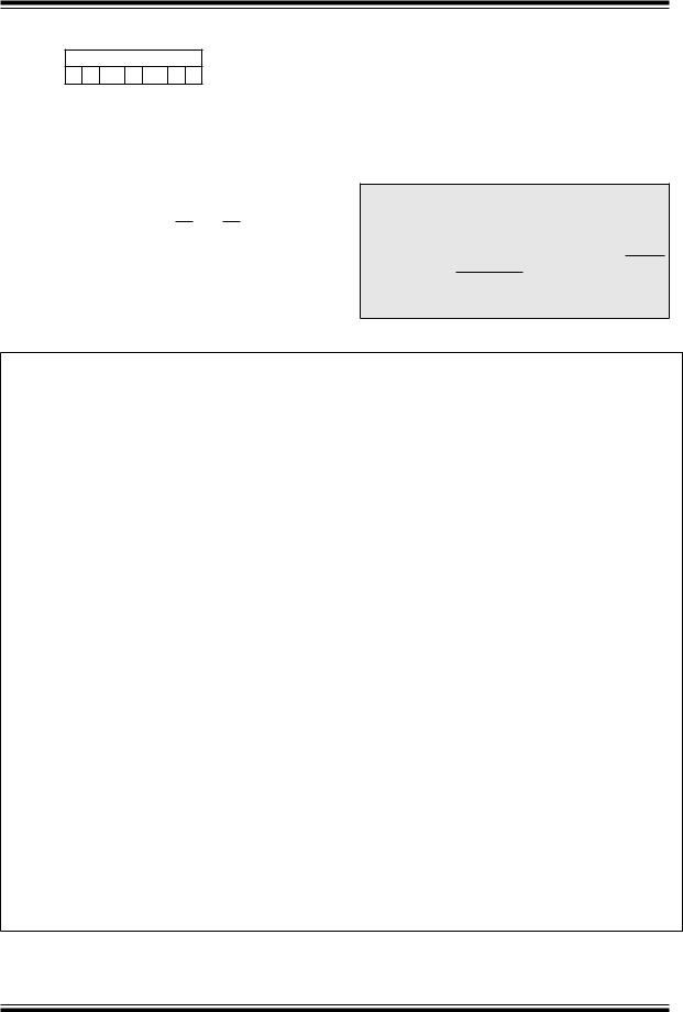
PIC16C7X
4.2.2.1STATUS REGISTER
Applicable Devices
72 73 73A 74 74A 76 77
The STATUS register, shown in Figure 4-7, contains the arithmetic status of the ALU, the RESET status and the bank select bits for data memory.
The STATUS register can be the destination for any instruction, as with any other register. If the STATUS register is the destination for an instruction that affects the Z, DC or C bits, then the write to these three bits is disabled. These bits are set or cleared according to the device logic. Furthermore, the TO and PD bits are not writable. Therefore, the result of an instruction with the STATUS register as destination may be different than intended.
For example, CLRF STATUS will clear the upper-three bits and set the Z bit. This leaves the STATUS register as 000u u1uu (where u = unchanged).
It is recommended, therefore, that only BCF, BSF, SWAPF and MOVWF instructions are used to alter the STATUS register because these instructions do not affect the Z, C or DC bits from the STATUS register. For other instructions, not affecting any status bits, see the "Instruction Set Summary."
Note 1: For those devices that do not use bits IRP and RP1 (STATUS<7:6>), maintain these bits clear to ensure upward compatibility with future products.
Note 2: The C and DC bits operate as a borrow and digit borrow bit, respectively, in subtraction. See the SUBLW and SUBWF instructions for examples.
FIGURE 4-7: STATUS REGISTER (ADDRESS 03h, 83h, 103h, 183h)
R/W-0 |
R/W-0 |
R/W-0 |
R-1 |
R-1 |
R/W-x |
R/W-x |
R/W-x |
|
|
||||
IRP |
RP1 |
RP0 |
|
TO |
|
|
PD |
|
Z |
DC |
C |
|
R = Readable bit |
bit7 |
|
|
|
|
|
|
|
|
|
|
bit0 |
|
W = Writable bit |
|
|
|
|
|
|
|
|
|
|
|
|
|
U = Unimplemented bit, |
|
|
|
|
|
|
|
|
|
|
|
|
|
read as ‘0’ |
|
|
|
|
|
|
|
|
|
|
|
|
|
- n = Value at POR reset |
bit 7: IRP: Register Bank Select bit (used for indirect addressing) 1 = Bank 2, 3 (100h - 1FFh)
0 = Bank 0, 1 (00h - FFh)
bit |
6-5: RP1:RP0: Register Bank Select bits (used for direct addressing) |
||||||||||||
|
|
11 = Bank 3 (180h - 1FFh) |
|||||||||||
|
|
10 = Bank 2 (100h - 17Fh) |
|||||||||||
|
|
01 = Bank 1 (80h - FFh) |
|||||||||||
|
|
00 = Bank 0 (00h - 7Fh) |
|||||||||||
|
|
Each bank is 128 bytes |
|||||||||||
bit |
4: |
|
: Time-out bit |
||||||||||
TO |
|||||||||||||
|
|
1 |
= After power-up, CLRWDT instruction, or SLEEP instruction |
||||||||||
|
|
0 |
= A WDT time-out occurred |
||||||||||
bit |
3: |
|
: Power-down bit |
||||||||||
PD |
|||||||||||||
|
|
1 |
= After power-up or by the CLRWDT instruction |
||||||||||
|
|
0 |
= By execution of the SLEEP instruction |
||||||||||
bit |
2: |
Z: Zero bit |
|||||||||||
|
|
1 |
= The result of an arithmetic or logic operation is zero |
||||||||||
|
|
0 |
= The result of an arithmetic or logic operation is not zero |
||||||||||
bit |
|
|
|
|
|
|
|
|
|
||||
1: DC: Digit carry/borrow |
bit (ADDWF, ADDLW,SUBLW,SUBWF instructions) (for borrow the polarity is reversed) |
||||||||||||
|
|
1 |
= A carry-out from the 4th low order bit of the result occurred |
||||||||||
|
|
0 |
= No carry-out from the 4th low order bit of the result |
||||||||||
bit |
0: |
|
|
|
bit (ADDWF, ADDLW,SUBLW,SUBWF instructions) |
||||||||
C: Carry/borrow |
|||||||||||||
|
|
1 |
= A carry-out from the most significant bit of the result occurred |
||||||||||
|
|
0 |
= No carry-out from the most significant bit of the result occurred |
||||||||||
|
|
Note: For |
|
the polarity is reversed. A subtraction is executed by adding the two’s complement of the |
|||||||||
|
|
borrow |
|||||||||||
|
|
second operand. For rotate (RRF, RLF) instructions, this bit is loaded with either the high or low order bit of |
|||||||||||
|
|
the source register. |
|||||||||||
DS30390E-page 30 |
1997 Microchip Technology Inc. |
 Loading...