


Microchip Technology Inc PIC16F873-04-L, PIC16F873-04-P, PIC16F873-04-PQ, PIC16F873-04-PT, PIC16F873-04-SO Datasheet
...PIC16F87X
Data Sheet
28/40-Pin 8-Bit CMOS FLASH
Microcontrollers
2001 Microchip Technology Inc. |
DS30292C |

“All rights reserved. Copyright © 2001, Microchip Technology Incorporated, USA. Information contained in this publication regarding device applications and the like is intended through suggestion only and may be superseded by updates. No representation or warranty is given and no liability is assumed by Microchip Technology Incorporated with respect to the accuracy or use of such information, or infringement of patents or other intellectual property rights arising from such use or otherwise. Use of Microchip’s products as critical components in life support systems is not authorized except with express written approval by Microchip. No licenses are conveyed, implicitly or otherwise, under any intellectual property rights. The Microchip logo and name are registered trademarks of Microchip Technology Inc. in the U.S.A. and other countries. All rights reserved. All other trademarks mentioned herein are the property of their respective companies. No licenses are conveyed, implicitly or otherwise, under any intellectual property rights.”
Trademarks
The Microchip name, logo, PIC, PICmicro, PICMASTER, PICSTART, PRO MATE, KEELOQ, SEEVAL, MPLAB and The Embedded Control Solutions Company are registered trademarks of Microchip Technology Incorporated in the U.S.A. and other countries.
Total Endurance, ICSP, In-Circuit Serial Programming, FilterLab, MXDEV, microID, FlexROM, fuzzyLAB, MPASM, MPLINK, MPLIB, PICDEM, ICEPIC, Migratable Memory, FanSense, ECONOMONITOR and SelectMode are trademarks of Microchip Technology Incorporated in the U.S.A.
Serialized Quick Term Programming (SQTP) is a service mark of Microchip Technology Incorporated in the U.S.A.
All other trademarks mentioned herein are property of their respective companies.
© 2001, Microchip Technology Incorporated, Printed in the U.S.A., All Rights Reserved.
Microchip received QS-9000 quality system certification for its worldwide headquarters, design and wafer fabrication facilities in Chandler and Tempe, Arizona in July 1999. The Company’s quality system processes and procedures are QS-9000 compliant for its PICmicro® 8-bit MCUs, KEELOQ® code hopping devices, Serial EEPROMs and microperipheral products. In addition, Microchip’s quality system for the design and manufacture of development systems is ISO 9001 certified.
DS30292C - page ii |
2001 Microchip Technology Inc. |

PIC16F87X
28/40-Pin 8-Bit CMOS FLASH Microcontrollers
Devices Included in this Data Sheet:
• |
PIC16F873 |
• |
PIC16F876 |
• |
PIC16F874 |
• |
PIC16F877 |
Microcontroller Core Features:
•High performance RISC CPU
•Only 35 single word instructions to learn
•All single cycle instructions except for program branches which are two cycle
•Operating speed: DC - 20 MHz clock input
DC - 200 ns instruction cycle
•Up to 8K x 14 words of FLASH Program Memory, Up to 368 x 8 bytes of Data Memory (RAM)
Up to 256 x 8 bytes of EEPROM Data Memory
•Pinout compatible to the PIC16C73B/74B/76/77
•Interrupt capability (up to 14 sources)
•Eight level deep hardware stack
•Direct, indirect and relative addressing modes
•Power-on Reset (POR)
•Power-up Timer (PWRT) and Oscillator Start-up Timer (OST)
•Watchdog Timer (WDT) with its own on-chip RC oscillator for reliable operation
•Programmable code protection
•Power saving SLEEP mode
•Selectable oscillator options
•Low power, high speed CMOS FLASH/EEPROM technology
•Fully static design
•In-Circuit Serial Programming (ICSP) via two pins
•Single 5V In-Circuit Serial Programming capability
•In-Circuit Debugging via two pins
•Processor read/write access to program memory
•Wide operating voltage range: 2.0V to 5.5V
•High Sink/Source Current: 25 mA
•Commercial, Industrial and Extended temperature ranges
•Low-power consumption:
-< 0.6 mA typical @ 3V, 4 MHz
-20 A typical @ 3V, 32 kHz
-< 1 A typical standby current
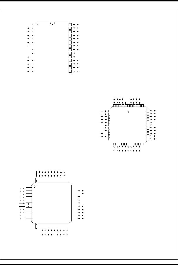
Pin Diagram
PDIP
|
|
|
|
|
|
|
|
|
|
|
|
|
|
|
|
|
|
|
|
|
|
|
|
|
|
|
|
MCLR/VPP |
|
|
|
|
|
|
|
1 |
|
40 |
|
|
|
|
|
RB7/PGD |
|||||||||
|
RA0/AN0 |
|
|
|
|
|
|
2 |
|
39 |
|
|
|
|
|
RB6/PGC |
||||||||||
|
RA1/AN1 |
|
|
|
|
|
|
3 |
|
38 |
|
|
|
|
|
RB5 |
||||||||||
RA2/AN2/VREF- |
|
|
|
|
|
|
4 |
|
37 |
|
|
|
|
|
RB4 |
|||||||||||
RA3/AN3/VREF+ |
|
|
|
|
|
|
5 |
|
36 |
|
|
|
|
|
RB3/PGM |
|||||||||||
RA4/T0CKI |
|
|
|
|
|
|
6 |
|
35 |
|
|
|
|
|
RB2 |
|||||||||||
|
|
|
|
|
|
|
|
|
|
|
|
|
|
7 |
|
34 |
|
|
|
|
|
RB1 |
||||
RA5/AN4/SS |
|
|
|
|
|
|
|
|
|
|
|
PIC16F877/874 |
|
|
|
|
|
|||||||||
|
|
|
|
|
|
|
|
|
|
|
|
|
|
|||||||||||||
|
|
|
|
|
|
|
|
|
|
|
|
|
|
|
|
|
|
|
|
|
|
|
|
|
|
|
RE0/RD/AN5 |
|
|
|
|
|
|
8 |
|
33 |
|
|
|
|
|
RB0/INT |
|||||||||||
|
|
|
|
|
|
|
|
|
|
|
|
|
|
|
|
|
|
|
|
|
|
|||||
RE1/WR/AN6 |
|
|
|
|
|
|
9 |
|
32 |
|
|
|
|
|
VDD |
|||||||||||
|
|
|
|
|
|
|
|
|
|
|
|
|
|
|
|
|
|
|
|
|
||||||
RE2/CS/AN7 |
|
|
|
|
|
|
10 |
|
31 |
|
|
|
|
|
VSS |
|||||||||||
|
|
|
|
|
|
VDD |
|
|
|
|
|
11 |
|
30 |
|
|
|
|
|
RD7/PSP7 |
||||||
|
|
|
|
|
|
VSS |
|
|
|
12 |
|
29 |
|
|
|
|
|
RD6/PSP6 |
||||||||
OSC1/CLKIN |
|
|
|
|
|
|
13 |
|
28 |
|
|
|
|
|
RD5/PSP5 |
|||||||||||
OSC2/CLKOUT |
|
|
|
|
|
14 |
|
27 |
|
|
|
|
|
RD4/PSP4 |
||||||||||||
RC0/T1OSO/T1CKI |
|
|
|
|
|
15 |
|
26 |
|
|
|
|
|
RC7/RX/DT |
||||||||||||
RC1/T1OSI/CCP2 |
|
|
|
|
|
16 |
|
25 |
|
|
|
|
|
RC6/TX/CK |
||||||||||||
RC2/CCP1 |
|
|
|
|
|
17 |
|
24 |
|
|
|
|
|
RC5/SDO |
||||||||||||
RC3/SCK/SCL |
|
|
|
|
|
18 |
|
23 |
|
|
|
|
|
RC4/SDI/SDA |
||||||||||||
|
RD0/PSP0 |
|
|
|
|
|
19 |
|
22 |
|
|
|
|
|
RD3/PSP3 |
|||||||||||
|
RD1/PSP1 |
|
|
|
|
|
20 |
|
21 |
|
|
|
|
|
RD2/PSP2 |
|||||||||||
|
|
|
|
|
|
|
|
|
|
|
|
|
|
|
|
|
|
|
|
|
|
|
|
|
|
|
Peripheral Features:
• Timer0: 8-bit timer/counter with 8-bit prescaler
• Timer1: 16-bit timer/counter with prescaler, can be incremented during SLEEP via external crystal/clock
• Timer2: 8-bit timer/counter with 8-bit period register, prescaler and postscaler
• Two Capture, Compare, PWM modules
- Capture is 16-bit, max. resolution is 12.5 ns
- Compare is 16-bit, max. resolution is 200 ns
- PWM max. resolution is 10-bit
• 10-bit multi-channel Analog-to-Digital converter
• Synchronous Serial Port (SSP) with SPI (Master mode) and I2C (Master/Slave)
• Universal Synchronous Asynchronous Receiver Transmitter (USART/SCI) with 9-bit address detection
• Parallel Slave Port (PSP) 8-bits wide, with external RD, WR and CS controls (40/44-pin only)
• Brown-out detection circuitry for Brown-out Reset (BOR)
|
|
2001 Microchip Technology Inc. |
DS30292C-page 1 |
PIC16F87X
Pin Diagrams
PDIP, SOIC
|
|
|
|
|
|
|
|
|
|
1 |
MCLR/VPP |
|
|
|
|||||||
|
RA0/AN0 |
|
|
|
|
2 |
||||
|
||||||||||
|
RA1/AN1 |
|
|
|
|
3 |
||||
RA2/AN2/VREF- |
|
|
|
|
4 |
|||||
|
|
|||||||||
|
||||||||||
RA3/AN3/VREF+ |
|
|
|
|
5 |
|||||
|
||||||||||
RA4/T0CKI |
|
|
|
|
6 |
|||||
|
||||||||||
RA5/AN4/SS |
|
|
|
|
|
|
7 |
|||
|
|
|||||||||
|
||||||||||
|
|
VSS |
|
|
|
8 |
||||
|
||||||||||
OSC1/CLKIN |
|
|
|
|
9 |
|||||
|
|
|||||||||
|
||||||||||
OSC2/CLKOUT |
|
|
|
10 |
||||||
|
|
|||||||||
RC0/T1OSO/T1CKI |
|
|
|
|
11 |
|||||
|
|
|
||||||||
RC1/T1OSI/CCP2 |
|
|
|
12 |
||||||
|
|
|||||||||
RC2/CCP1 |
|
|
|
|
13 |
|||||
RC3/SCK/SCL |
|
|
|
|
14 |
|||||
|
|
|
|
|
|
|
|
|
|
|
PIC16F876/873
28 |
|
|
|
RB7/PGD |
|
|
|
|
|
|
|
|
|
|
|
|
|||
27 |
|
|
|
RB6/PGC |
|
|
|
|
|
|
|
|
|
|
|
||||
26 |
|
|
|
RB5 |
|
|
|
|
|
|
|
|
|
|
|
||||
25 |
|
|
|
RB4 |
|
|
|
|
|
|
|
|
|
|
|
||||
24 |
|
|
|
RB3/PGM |
|
|
|
|
|
|
|
|
|
|
|
||||
23 |
|
|
|
RB2 |
|
|
|
|
|
|
|
|
|
|
|
||||
22 |
|
|
|
RB1 |
|
|
|
|
|
|
|
|
|
|
|
||||
21 |
|
|
|
RB0/INT |
|
|
|
|
|
|
|
|
|
|
|
|
|||
20 |
|
|
|
VDD |
|
|
|
|
|
|
|
|
|
|
|
|
|||
19 |
|
|
|
VSS |
|
|
|
|
|
|
|
|
|
|
|
|
|||
18 |
|
|
|
RC7/RX/DT |
|
|
|
|
|
|
|
|
|
|
|
|
|||
17 |
|
|
|
RC6/TX/CK |
|
|
|
|
|
|
|
|
|
|
|
|
|||
16 |
|
|
|
RC5/SDO |
|
|
|
|
|
|
|
|
|
|
|
|
|||
15 |
|
|
|
RC4/SDI/SDA |
+ |
||||
|
|
|
|||||||
|
|
|
|
|
|
||||
|
|
|
|
PLCC |
|
|
RA3/AN3/VREF |
||
|
|
|
|
|
|
|
|
||
|
|
|
|
|
|
|
|||
|
|
|
|
|
|
|
|
||
|
|
|
|
RA4/T0CKI |
6 |
||||
|
|
|
|
|
|
|
|
||
|
|
|
|
RA5/AN4/SS |
7 |
|
|||
|
|
|
|
|
8 |
|
|||
|
|
|
|
RE0/RD/AN5 |
|
|
|||
|
|
|
|
|
|
|
|
||
|
|
|
|
RE1/WR/AN6 |
|
9 |
|
||
|
|
|
|
RE2/CS/AN7 |
|
10 |
|
||
|
|
|
|
11 |
|
||||
|
|
|
|
VDD |
|
|
|||
|
|
|
|
|
|
12 |
|
||
|
|
|
|
VSS |
|
|
|
||
|
|
|
|
|
|
|
|
|
|
|
|
|
|
OSC1/CLKIN |
|
|
13 |
|
|
|
|
|
|
|
14 |
|
|||
|
|
|
|
OSC2/CLKOUT |
|
||||
|
|
|
|
|
|
15 |
|
||
|
|
RC0/T1OSO/T1CK1 |
|
|
|||||
|
|
|
|
|
|
||||
|
|
16 |
|
||||||
|
|
|
|
NC |
|
||||
|
|
|
|
17 |
|
||||
|
|
|
|
|
|
18 |
|||
RA2/AN2/VREF- RA1/AN1 RA0/AN0 |
|
MCLR/VPP NC |
RB7/PGD RB6/PGC |
RB5 RB4 |
||||||||
|
||||||||||||
|
|
|
|
|
|
|
|
|
|
|||
|
|
|
|
|
|
|
|
|
|
|
|
|
|
|
|
|
|
|
|
|
|
|
|
||
5 4 3 2 1 |
44 43 |
42 41 |
||||||||||
PIC16F877
PIC16F874
19 |
20 21 22 |
23 24 |
25 26 27 |
40 NC
28
39 |
|
|
RB3/PGM |
|
|||
38 |
|
|
RB2 |
|
|||
37 |
|
|
RB1 |
|
|||
36 |
|
|
RB0/INT |
|
|||
35 |
|
|
VDD |
|
|
||
34 |
|
|
VSS |
|
|
||
33 |
|
|
RD7/PSP7 |
|
|
||
32 |
|
|
RD6/PSP6 |
|
|
||
31 |
|
|
RD5/PSP5 |
|
|
||
30 |
|
|
RD4/PSP4 |
|
|||
29 |
|
|
RC7/RX/DT |
|
|
QFP
RC7/RX/DT 


 RD4/PSP4


 RD5/PSP5


 RD6/PSP6


 RD7/PSP7


VSS
VDD
RB0/INT 

 RB1
RB1 

 RB2
RB2 


RB3/PGM 


RC6/TX/CK
44 1
2
3
4
5
6
7
8
9
10
11 12
NC
|
|
|
|
RC4/SDI/SDA |
|
|
|
|
|
|
|
|
|
|
RC3/SCK/SCL |
|
|
|
RC1/T1OSI/CCP2 |
|
|
|
|
|
|
|
|
|
|
|
|
|
|
|
|
|
|
|
|
|
|
|
|
|
|
RC5/SDO |
|
RD3/PSP3 |
RD2/PSP2 |
|
RD1/PSP1 |
|
|
RD0/PSP0 |
|
|
RC2/CCP1 |
NC |
|
|
|
|
|
|
RC1/T1OSI/CCP2 RC2/CCP1 RC3/SCK/SCL RD0/PSP0 RD1/PSP1 RD2/PSP2 RD3/PSP3 RC4/SDI/SDA RC5/SDO RC6/TX/CK NC |
||||||||||||||||||||||||||
|
|
|
|
|
|
|
|
|
|
|
|
|
|
|
|
|
|
|
|
|
|
|
|
|
|
|
|
|
|
|
|
|
|
|
|||||||||||
|
|
|
|
|
|
|
|
|
|
|
|
|
|
|
|
|
|
|
|
|
|
|
|
|
|
|
|
|
|
|
|
|
|
|
|
|
|
|
|
|
|
|
|
|
|
|
|
|
|
|
|
|
|
|
|
|
|
|
|
|
|
|
|
|
|
|
|
|
|
|
|
|
|
|
|
|
|
|
|
|
|
|
|
|
|
|
|
|
|
|
|
|
|
|
|
|
|
|
|
|
|
|
|
|
|
|
|
|
|
|
|
|
|
|
|
|
|
|
|
|
|
|
|
|
|
|
|
|
|
|
|
|
|
|
|
|
|
|
|
|
|
|
|
|
|
|
|
|
|
|
|
|
|
|
|
|
|
|
|
|
|
|
|
|
|
|
|
|
|
|
|
|
|
|
|
|
|
|
|
|
|
|
|
43 |
|
42 41 |
40 |
|
39 |
|
38 |
|
37 |
36 |
35 |
34 |
|
|
|
|
|
|
|
|
|
NC |
|||||||||||||||||||||||
|
|
|
|
|
|
|
|
|
|
|
|
|
|
|
|
|
|
|
|
|
33 |
|
|
|
|
|
|
|
|
|
|||||||||||||||
|
|
|
|
|
|
|
|
|
|
|
|
|
|
|
|
|
|
|
|
|
|
|
|
|
|
||||||||||||||||||||
|
|
|
|
|
|
|
|
|
|
|
|
|
|
|
|
|
|
|
|
|
32 |
|
|
|
|
|
|
|
|
|
RC0/T1OSO/T1CKI |
||||||||||||||
|
|
|
|
|
|
|
|
|
|
|
|
|
|
|
|
|
|
|
|
|
|
|
|
|
|
|
|
|
|||||||||||||||||
|
|
|
|
|
|
|
|
|
|
|
|
|
|
|
|
|
|
|
|
|
31 |
|
|
|
|
|
|
|
|
|
OSC2/CLKOUT |
||||||||||||||
|
|
|
|
|
|
|
|
|
|
|
|
|
|
|
|
|
|
|
|
|
30 |
|
|
|
|
|
|
|
|
|
OSC1/CLKIN |
||||||||||||||
|
|
|
PIC16F877 |
|
|
|
29 |
|
|
|
|
|
|
|
|
|
VSS |
||||||||||||||||||||||||||||
|
|
|
|
|
|
|
|
|
|
|
|
|
|
|
|||||||||||||||||||||||||||||||
|
|
|
PIC16F874 |
|
|
|
28 |
|
|
|
|
|
|
|
|
|
VDD |
|
|
||||||||||||||||||||||||||
|
|
|
|
|
|
27 |
|
|
|
|
|
|
|
|
|
RE2/AN7/CS |
|||||||||||||||||||||||||||||
|
|
|
|
|
|
|
|
|
|
|
|
|
|
|
|
|
|
|
|
|
|
|
|
|
|
|
|
|
|
||||||||||||||||
|
|
|
|
|
|
|
|
|
|
|
|
|
|
|
|
|
|
|
|
|
26 |
|
|
|
|
|
|
|
|
|
RE1/AN6/WR |
||||||||||||||
|
|
|
|
|
|
|
|
|
|
|
|
|
|
|
|
|
|
|
|
|
25 |
|
|
|
|
|
|
|
|
|
RE0/AN5/RD |
||||||||||||||
|
|
|
|
|
|
|
|
|
|
|
|
|
|
|
|
|
|
|
|
|
24 |
|
|
|
|
|
|
|
|
|
RA5/AN4/SS |
||||||||||||||
|
|
|
|
|
|
|
|
|
|
|
|
|
|
|
|
|
|
|
|
|
|
|
|
|
|
|
|
|
|
||||||||||||||||
13 |
14 |
15 |
16 |
17 |
18 |
19 |
20 |
|
|
|
23 |
|
|
|
|
|
|
|
|
|
RA4/T0CKI |
||||||||||||||||||||||||
21 22 |
|
|
|
|
|
|
|
|
|
|
|
|
|
|
|
|
|
|
|
|
|
|
|||||||||||||||||||||||
|
|
|
|
|
|
|
|
|
|
|
|
|
|
|
|
|
|
|
|
|
|
|
|
|
|
|
|
|
|
|
|
|
|
|
|
|
|
|
|
|
|||||
|
|
|
|
|
|
|
|
|
|
|
|
|
|
|
|
|
|
|
|
|
|
|
|
|
|
|
|
|
|
|
|
|
|
|
|
|
|
|
|
|
|
|
|
|
|
|
|
|
|
|
|
|
|
|
|
|
|
|
|
|
|
|
|
|
|
|
|
|
|
|
|
|
|
|
|
|
|
|
|
|
|
|
|
|
|
|
|
|
|
|
|
|
|
|
|
|
|
|
|
|
|
|
|
|
|
|
|
|
|
|
|
|
|
|
|
|
|
|
|
|
|
|
|
|
|
|
|
||||||||||
|
|
|
|
|
|
|
|
|
|
|
|
|
|
|
|
|
|
|
|
|
|
|
|
|
|
|
|
|
|
|
|
|
|
|
|
|
|||||||||
NC |
RB4 |
RB5 |
RB6/PGC |
RB7/PGD |
|
|
|
RA0/AN0 |
RA1/AN1 |
|
|
RA3/AN3/VREF+ |
|
|
|
|
|
|
|
|
|
|
|
|
|
|
|
|
|
||||||||||||||||
|
MCLR/VPP |
RA2/AN2/VREF- |
|
|
|
|
|
|
|
|
|
|
|
|
|
|
|
|
|
||||||||||||||||||||||||||
|
|
|
|
|
|
|
|
|
|
|
|
|
|
|
|
|
|
|
|
|
|
|
|
||||||||||||||||||||||
|
|
|
|
|
|
|
|
|
|
|
|
|
|
|
|
|
|
|
|
|
|
|
|
|
|
|
|
|
|
|
|
|
|
|
|||||||||||
DS30292C-page 2 |
2001 Microchip Technology Inc. |

PIC16F87X
Key Features |
|
|
|
|
|
PICmicro™ Mid-Range Reference |
PIC16F873 |
PIC16F874 |
PIC16F876 |
PIC16F877 |
|
Manual (DS33023) |
|
|
|
|
|
|
|
|
|
|
|
|
|
|
|
|
|
Operating Frequency |
DC - 20 MHz |
DC - 20 MHz |
DC - 20 MHz |
DC - 20 MHz |
|
|
|
|
|
|
|
RESETS (and Delays) |
POR, BOR |
POR, BOR |
POR, BOR |
POR, BOR |
|
|
(PWRT, OST) |
(PWRT, OST) |
(PWRT, OST) |
(PWRT, OST) |
|
|
|
|
|
|
|
FLASH Program Memory |
4K |
4K |
8K |
8K |
|
(14-bit words) |
|||||
|
|
|
|
||
|
|
|
|
|
|
Data Memory (bytes) |
192 |
192 |
368 |
368 |
|
|
|
|
|
|
|
EEPROM Data Memory |
128 |
128 |
256 |
256 |
|
|
|
|
|
|
|
Interrupts |
13 |
14 |
13 |
14 |
|
|
|
|
|
|
|
I/O Ports |
Ports A,B,C |
Ports A,B,C,D,E |
Ports A,B,C |
Ports A,B,C,D,E |
|
|
|
|
|
|
|
Timers |
3 |
3 |
3 |
3 |
|
|
|
|
|
|
|
Capture/Compare/PWM Modules |
2 |
2 |
2 |
2 |
|
|
|
|
|
|
|
Serial Communications |
MSSP, USART |
MSSP, USART |
MSSP, USART |
MSSP, USART |
|
|
|
|
|
|
|
Parallel Communications |
— |
PSP |
— |
PSP |
|
|
|
|
|
|
|
10-bit Analog-to-Digital Module |
5 input channels |
8 input channels |
5 input channels |
8 input channels |
|
|
|
|
|
|
|
Instruction Set |
35 instructions |
35 instructions |
35 instructions |
35 instructions |
|
|
|
|
|
|
2001 Microchip Technology Inc. |
DS30292C-page 3 |

PIC16F87X |
|
|
Table of Contents |
|
|
1.0 |
Device Overview ................................................................................................................................................... |
5 |
2.0 |
Memory Organization.......................................................................................................................................... |
11 |
3.0 |
I/O Ports .............................................................................................................................................................. |
29 |
4.0 |
Data EEPROM and FLASH Program Memory.................................................................................................... |
41 |
5.0 |
Timer0 Module .................................................................................................................................................... |
47 |
6.0 |
Timer1 Module .................................................................................................................................................... |
51 |
7.0 |
Timer2 Module .................................................................................................................................................... |
55 |
8.0 |
Capture/Compare/PWM Modules ....................................................................................................................... |
57 |
9.0 |
Master Synchronous Serial Port (MSSP) Module ............................................................................................... |
65 |
10.0 |
Addressable Universal Synchronous Asynchronous Receiver Transmitter (USART) ........................................ |
95 |
11.0 |
Analog-to-Digital Converter (A/D) Module......................................................................................................... |
111 |
12.0 |
Special Features of the CPU............................................................................................................................. |
119 |
13.0 |
Instruction Set Summary................................................................................................................................... |
135 |
14.0 |
Development Support ....................................................................................................................................... |
143 |
15.0 |
Electrical Characteristics................................................................................................................................... |
149 |
16.0 |
DC and AC Characteristics Graphs and Tables................................................................................................ |
177 |
17.0 |
Packaging Information ...................................................................................................................................... |
189 |
Appendix A: Revision History .................................................................................................................................... |
197 |
|
Appendix B: Device Differences ................................................................................................................................ |
197 |
|
Appendix C: Conversion Considerations ................................................................................................................... |
198 |
|
Index |
.......................................................................................................................................................................... |
199 |
On-Line Support ......................................................................................................................................................... |
207 |
|
Reader Response ...................................................................................................................................................... |
208 |
|
PIC16F87X Product Identification System ................................................................................................................. |
209 |
|
TO OUR VALUED CUSTOMERS
It is our intention to provide our valued customers with the best documentation possible to ensure successful use of your Microchip products. To this end, we will continue to improve our publications to better suit your needs. Our publications will be refined and enhanced as new volumes and updates are introduced.
If you have any questions or comments regarding this publication, please contact the Marketing Communications Department via E-mail at docerrors@mail.microchip.com or fax the Reader Response Form in the back of this data sheet to (480) 792-4150. We welcome your feedback.
Most Current Data Sheet
To obtain the most up-to-date version of this data sheet, please register at our Worldwide Web site at: http://www.microchip.com
You can determine the version of a data sheet by examining its literature number found on the bottom outside corner of any page. The last character of the literature number is the version number, (e.g., DS30000A is version A of document DS30000).
Errata
An errata sheet, describing minor operational differences from the data sheet and recommended workarounds, may exist for current devices. As device/documentation issues become known to us, we will publish an errata sheet. The errata will specify the revision of silicon and revision of document to which it applies.
To determine if an errata sheet exists for a particular device, please check with one of the following:
•Microchip’s Worldwide Web site; http://www.microchip.com
•Your local Microchip sales office (see last page)
•The Microchip Corporate Literature Center; U.S. FAX: (480) 792-7277
When contacting a sales office or the literature center, please specify which device, revision of silicon and data sheet (include literature number) you are using.
Customer Notification System
Register on our web site at www.microchip.com/cn to receive the most current information on all of our products.
DS30292C-page 4 |
2001 Microchip Technology Inc. |

PIC16F87X
1.0DEVICE OVERVIEW
This document contains device specific information. Additional information may be found in the PICmicro™ Mid-Range Reference Manual (DS33023), which may be obtained from your local Microchip Sales Representative or downloaded from the Microchip website. The Reference Manual should be considered a complementary document to this data sheet, and is highly recommended reading for a better understanding of the device architecture and operation of the peripheral modules.
There are four devices (PIC16F873, PIC16F874, PIC16F876 and PIC16F877) covered by this data sheet. The PIC16F876/873 devices come in 28-pin packages and the PIC16F877/874 devices come in 40-pin packages. The Parallel Slave Port is not implemented on the 28-pin devices.
The following device block diagrams are sorted by pin number; 28-pin for Figure 1-1 and 40-pin for Figure 1-2. The 28-pin and 40-pin pinouts are listed in Table 1-1 and Table 1-2, respectively.
FIGURE 1-1: |
PIC16F873 AND PIC16F876 BLOCK DIAGRAM |
||||
|
|
|
|
|
|
|
Device |
Program |
Data Memory |
Data |
|
|
FLASH |
EEPROM |
|
||
|
|
|
|
||
|
|
|
|
|
|
|
PIC16F873 |
4K |
192 Bytes |
128 Bytes |
|
|
|
|
|
|
|
|
PIC16F876 |
8K |
368 Bytes |
256 Bytes |
|
|
|
|
|
|
|
|
|
13 |
|
Data Bus |
8 |
PORTA |
|
|
|
Program Counter |
|
|
RA0/AN0 |
||
|
|
|
|
|
|
|
|
|
FLASH |
|
|
|
|
|
RA1/AN1 |
|
Program |
|
|
|
RAM |
|
RA2/AN2/VREF- |
|
Memory |
8 Level Stack |
|
|
RA3/AN3/VREF+ |
||
|
|
|
File |
|
RA4/T0CKI |
||
|
|
(13-bit) |
|
Registers |
|
||
|
|
|
|
RA5/AN4/SS |
|||
|
|
|
|
|
|
|
|
Program |
14 |
|
|
RAM Addr(1) |
9 |
|
PORTB |
Bus |
|
|
|
||||
|
|
|
RB0/INT |
||||
|
|
|
|
Addr MUX |
|
||
|
Instruction reg |
|
|
|
RB1 |
||
|
|
|
|
|
|
||
|
|
|
|
|
|
RB2 |
|
|
|
Direct Addr |
7 |
|
|
Indirect |
|
|
|
|
8 |
RB3/PGM |
|||
|
|
|
|
Addr |
|||
|
|
|
|
|
RB4 |
||
|
|
|
|
|
|
|
|
|
|
|
|
|
FSR reg |
RB5 |
|
|
|
|
|
|
|
|
RB6/PGC |
|
|
8 |
|
|
STATUS reg |
RB7/PGD |
|
|
|
|
|
|
|
PORTC |
|
|
|
|
|
|
|
|
|
|
|
Power-up |
|
3 |
MUX |
RC0/T1OSO/T1CKI |
|
|
|
|
RC1/T1OSI/CCP2 |
||||
|
|
|
|
||||
|
|
Timer |
|
|
|
|
RC2/CCP1 |
|
Instruction |
Oscillator |
|
|
|
|
RC3/SCK/SCL |
|
Decode & |
Start-up Timer |
|
ALU |
|
RC4/SDI/SDA |
|
|
Control |
Power-on |
|
|
RC5/SDO |
||
|
|
|
|
|
|||
|
|
|
8 |
|
|
RC6/TX/CK |
|
|
|
Reset |
|
|
|
||
|
Timing |
Watchdog |
|
|
|
|
RC7/RX/DT |
|
|
W reg |
|
|
|||
|
Generation |
Timer |
|
|
|
||
OSC1/CLKIN |
|
Brown-out |
|
|
|
|
|
OSC2/CLKOUT |
|
Reset |
|
|
|
|
|
|
|
In-Circuit |
|
|
|
|
|
|
|
Debugger |
|
|
|
|
|
|
|
Low Voltage |
|
|
|
|
|
|
|
Programming |
|
|
|
|
|
MCLR VDD, VSS
Timer0 |
|
Timer1 |
|
Timer2 |
|
10-bit A/D |
|||||||
|
|
|
|
|
|
|
|
|
|
|
|
|
|
|
|
|
|
|
|
|
|
|
|
|
|
|
|
|
|
|
|
|
|
|
|
|
|
|
|
|
|
|
|
|
|
|
|
|
|
|
|
|
|
|
|
|
|
|
|
|
|
|
|
|
|
|
|
|
|
Data EEPROM |
|
CCP1,2 |
|
Synchronous |
|
USART |
|
|
Serial Port |
|
|||
|
|
|
|
|
|
|
|
|
|
|
|
|
|
Note 1: Higher order bits are from the STATUS register. |
|
|||||
2001 Microchip Technology Inc. |
DS30292C-page 5 |

PIC16F87X
FIGURE 1-2: |
PIC16F874 AND PIC16F877 BLOCK DIAGRAM |
||||
|
|
|
|
|
|
|
Device |
Program |
Data Memory |
Data |
|
|
FLASH |
EEPROM |
|
||
|
|
|
|
||
|
|
|
|
|
|
|
PIC16F874 |
4K |
192 Bytes |
128 Bytes |
|
|
|
|
|
|
|
|
PIC16F877 |
8K |
368 Bytes |
256 Bytes |
|
|
|
|
|
|
|
|
|
13 |
|
|
Data Bus |
8 |
PORTA |
|
|
FLASH |
Program Counter |
|
|
RA0/AN0 |
|||
|
|
|
|
|
|
|
||
|
Program |
|
|
|
|
|
|
RA1/AN1 |
|
|
|
|
|
|
|
RA2/AN2/VREF- |
|
|
Memory |
|
|
|
|
RAM |
|
|
|
|
|
|
|
|
RA3/AN3/VREF+ |
||
|
|
8 Level Stack |
|
|
||||
|
|
|
File |
|
||||
|
|
|
|
RA4/T0CKI |
||||
|
|
|
(13-bit) |
|
|
|
||
|
|
|
|
Registers |
|
|||
|
|
|
|
|
RA5/AN4/SS |
|||
|
|
|
|
|
|
|
|
|
Program |
14 |
|
|
|
RAM Addr(1) |
9 |
|
PORTB |
Bus |
|
|
|
|
||||
|
|
|
|
|
Addr MUX |
|
RB0/INT |
|
|
Instruction reg |
|
|
|
|
RB1 |
||
|
|
|
|
|
|
|
||
|
|
|
|
|
|
|
RB2 |
|
|
|
Direct Addr |
7 |
|
|
Indirect |
||
|
|
|
8 |
RB3/PGM |
||||
|
|
|
|
Addr |
||||
|
|
|
|
|
|
RB4 |
||
|
|
|
|
|
|
|
|
|
|
|
|
|
|
|
FSR reg |
RB5 |
|
|
|
|
|
|
|
|
|
RB6/PGC |
|
|
8 |
|
|
|
STATUS reg |
RB7/PGD |
|
|
|
|
|
|
|
|
PORTC |
|
|
|
|
|
|
|
|
|
|
|
|
|
|
|
3 |
|
|
RC0/T1OSO/T1CKI |
|
|
Power-up |
|
MUX |
RC1/T1OSI/CCP2 |
|||
|
|
|
|
|||||
|
|
Timer |
|
|
|
|
RC2/CCP1 |
|
|
Instruction |
Oscillator |
|
|
|
|
RC3/SCK/SCL |
|
|
|
|
|
|
RC4/SDI/SDA |
|||
|
Decode & |
Start-up Timer |
|
ALU |
|
|||
|
|
|
RC5/SDO |
|||||
|
Control |
|
|
|
|
|||
|
Power-on |
|
|
|
|
|||
|
|
|
|
|
RC6/TX/CK |
|||
|
|
|
8 |
|
|
|||
|
|
Reset |
|
|
|
|||
|
|
|
|
|
RC7/RX/DT |
|||
|
Timing |
Watchdog |
|
|
|
|
||
|
|
W reg |
|
|
||||
|
Generation |
Timer |
|
|
PORTD |
|||
OSC1/CLKIN |
|
|
|
|
||||
|
Brown-out |
|
|
|
|
RD0/PSP0 |
||
OSC2/CLKOUT |
|
Reset |
|
|
|
|
RD1/PSP1 |
|
|
|
In-Circuit |
|
|
|
|
RD2/PSP2 |
|
|
|
Debugger |
|
|
|
|
RD3/PSP3 |
|
|
|
Low-Voltage |
|
|
|
|
RD4/PSP4 |
|
|
|
|
|
|
|
RD5/PSP5 |
||
|
|
Programming |
|
Parallel Slave Port |
||||
|
|
|
|
|
|
|
|
RD6/PSP6 |
|
|
|
|
|
|
|
|
RD7/PSP7 |
|
|
|
|
|
|
|
|
PORTE |
|
|
MCLR |
VDD, VSS |
|
|
|
RE0/AN5/RD |
|
|
|
|
|
|
|
|
|
RE1/AN6/WR |
|
|
|
|
|
|
|
|
RE2/AN7/CS |
Timer0 |
Timer1 |
|
Timer2 |
|
10-bit A/D |
|
||
Data EEPROM |
|
CCP1,2 |
|
Synchronous |
|
USART |
|
|
Serial Port |
|
|||
|
|
|
|
|
|
|
|
|
|
|
|
|
|
Note 1: Higher order bits are from the STATUS register. |
|
|||||
DS30292C-page 6 |
2001 Microchip Technology Inc. |

|
|
|
|
|
|
|
|
|
|
|
PIC16F87X |
|
|
|
|
|
|
|
|
|
|
|
|
|
|
TABLE 1-1: |
PIC16F873 AND PIC16F876 PINOUT DESCRIPTION |
|||||||||||
|
|
|
|
|
|
|
|
|
|
|
|
|
|
|
Pin Name |
|
DIP |
|
SOIC |
I/O/P |
Buffer |
Description |
|||
|
|
|
Pin# |
|
Pin# |
Type |
Type |
|||||
|
|
|
|
|
|
|
|
|
||||
|
|
|
|
|
|
|
|
|
||||
|
|
|
|
|
|
|
|
|
||||
|
OSC1/CLKIN |
|
9 |
|
9 |
I |
ST/CMOS(3) |
Oscillator crystal input/external clock source input. |
||||
|
OSC2/CLKOUT |
|
10 |
|
10 |
O |
— |
Oscillator crystal output. Connects to crystal or resonator in |
||||
|
|
|
|
|
|
|
|
|
|
|
crystal oscillator mode. In RC mode, the OSC2 pin outputs |
|
|
|
|
|
|
|
|
|
|
|
|
CLKOUT which has 1/4 the frequency of OSC1, and denotes |
|
|
|
|
|
|
|
|
|
|
|
|
the instruction cycle rate. |
|
|
|
|
|
|
|
|
|
|
|
|
||
|
|
|
|
PP |
|
1 |
|
1 |
I/P |
ST |
Master Clear (Reset) input or programming voltage input. This |
|
|
MCLR/V |
|
|
|
||||||||
|
|
|
|
|
|
|
|
|
|
|
pin is an active low RESET to the device. |
|
|
|
|
|
|
|
|
|
|
|
|
|
|
|
|
|
|
|
|
|
|
|
|
|
PORTA is a bi-directional I/O port. |
|
|
RA0/AN0 |
|
2 |
|
2 |
I/O |
TTL |
RA0 can also be analog input0. |
||||
|
RA1/AN1 |
|
3 |
|
3 |
I/O |
TTL |
RA1 can also be analog input1. |
||||
|
RA2/AN2/VREF- |
|
4 |
|
4 |
I/O |
TTL |
RA2 can also be analog input2 or negative analog |
||||
|
|
|
|
|
|
|
|
|
|
|
reference voltage. |
|
|
RA3/AN3/VREF+ |
|
5 |
|
5 |
I/O |
TTL |
RA3 can also be analog input3 or positive analog |
||||
|
|
|
|
|
|
|
|
|
|
|
reference voltage. |
|
|
RA4/T0CKI |
|
6 |
|
6 |
I/O |
ST |
RA4 can also be the clock input to the Timer0 |
||||
|
|
|
|
|
|
|
|
|
|
|
module. Output is open drain type. |
|
|
|
|
|
|
7 |
|
7 |
I/O |
TTL |
RA5 can also be analog input4 or the slave select |
||
|
RA5/SS/AN4 |
|
|
|||||||||
|
|
|
|
|
|
|
|
|
|
|
for the synchronous serial port. |
|
|
|
|
|
|
|
|
|
|
|
|
|
|
|
|
|
|
|
|
|
|
|
|
|
PORTB is a bi-directional I/O port. PORTB can be software |
|
|
|
|
|
|
|
|
|
|
|
|
programmed for internal weak pull-up on all inputs. |
|
|
RB0/INT |
|
21 |
|
21 |
I/O |
TTL/ST(1) |
RB0 can also be the external interrupt pin. |
||||
|
RB1 |
|
22 |
|
22 |
I/O |
TTL |
|
|
|||
|
RB2 |
|
23 |
|
23 |
I/O |
TTL |
|
|
|||
|
RB3/PGM |
|
24 |
|
24 |
I/O |
TTL |
RB3 can also be the low voltage programming input. |
||||
|
RB4 |
|
25 |
|
25 |
I/O |
TTL |
Interrupt-on-change pin. |
||||
|
RB5 |
|
26 |
|
26 |
I/O |
TTL |
Interrupt-on-change pin. |
||||
|
RB6/PGC |
|
27 |
|
27 |
I/O |
TTL/ST(2) |
Interrupt-on-change pin or In-Circuit Debugger pin. Serial |
||||
|
|
|
|
|
|
|
|
|
|
|
programming clock. |
|
|
RB7/PGD |
|
28 |
|
28 |
I/O |
TTL/ST(2) |
Interrupt-on-change pin or In-Circuit Debugger pin. Serial |
||||
|
|
|
|
|
|
|
|
|
|
|
programming data. |
|
|
|
|
|
|
|
|
|
|
|
|
|
|
|
|
|
|
|
|
|
|
|
|
|
PORTC is a bi-directional I/O port. |
|
|
RC0/T1OSO/T1CKI |
11 |
|
11 |
I/O |
ST |
RC0 can also be the Timer1 oscillator output or Timer1 |
|||||
|
|
|
|
|
|
|
|
|
|
|
clock input. |
|
|
RC1/T1OSI/CCP2 |
|
12 |
|
12 |
I/O |
ST |
RC1 can also be the Timer1 oscillator input or Capture2 |
||||
|
|
|
|
|
|
|
|
|
|
|
input/Compare2 output/PWM2 output. |
|
|
RC2/CCP1 |
|
13 |
|
13 |
I/O |
ST |
RC2 can also be the Capture1 input/Compare1 output/ |
||||
|
|
|
|
|
|
|
|
|
|
|
PWM1 output. |
|
|
RC3/SCK/SCL |
|
14 |
|
14 |
I/O |
ST |
RC3 can also be the synchronous serial clock input/output |
||||
|
|
|
|
|
|
|
|
|
|
|
for both SPI and I2C modes. |
|
|
RC4/SDI/SDA |
|
15 |
|
15 |
I/O |
ST |
RC4 can also be the SPI Data In (SPI mode) or |
||||
|
|
|
|
|
|
|
|
|
|
|
data I/O (I2C mode). |
|
|
RC5/SDO |
|
16 |
|
16 |
I/O |
ST |
RC5 can also be the SPI Data Out (SPI mode). |
||||
|
RC6/TX/CK |
|
17 |
|
17 |
I/O |
ST |
RC6 can also be the USART Asynchronous Transmit or |
||||
|
|
|
|
|
|
|
|
|
|
|
Synchronous Clock. |
|
|
RC7/RX/DT |
|
18 |
|
18 |
I/O |
ST |
RC7 can also be the USART Asynchronous Receive or |
||||
|
|
|
|
|
|
|
|
|
|
|
Synchronous Data. |
|
|
|
|
|
|
|
|
|
|
||||
|
VSS |
|
8, 19 |
|
8, 19 |
P |
— |
Ground reference for logic and I/O pins. |
||||
|
|
|
|
|
|
|
|
|
||||
|
VDD |
|
20 |
|
20 |
P |
— |
Positive supply for logic and I/O pins. |
||||
|
|
|
|
|
|
|
|
|
||||
|
Legend: I = input |
|
O = output |
|
I/O = input/output |
P = power |
||||||
|
|
|
|
|
|
— = Not used |
TTL = TTL input |
ST = Schmitt Trigger input |
||||
Note 1: This buffer is a Schmitt Trigger input when configured as the external interrupt.
2:This buffer is a Schmitt Trigger input when used in Serial Programming mode.
3:This buffer is a Schmitt Trigger input when configured in RC oscillator mode and a CMOS input otherwise.
2001 Microchip Technology Inc. |
DS30292C-page 7 |

PIC16F87X
TABLE 1-2: |
PIC16F874 AND PIC16F877 PINOUT DESCRIPTION |
||||||||||
|
|
|
|
|
|
|
|
|
|
|
|
|
Pin Name |
|
DIP |
PLCC |
QFP |
I/O/P |
Buffer |
Description |
|||
|
|
Pin# |
Pin# |
Pin# |
Type |
Type |
|||||
|
|
|
|
|
|
|
|||||
|
|
|
|
|
|
|
|
||||
|
|
|
|
|
|
|
|
||||
OSC1/CLKIN |
|
13 |
14 |
30 |
I |
ST/CMOS(4) |
Oscillator crystal input/external clock source input. |
||||
OSC2/CLKOUT |
|
14 |
15 |
31 |
O |
— |
Oscillator crystal output. Connects to crystal or resonator |
||||
|
|
|
|
|
|
|
|
|
|
|
in crystal oscillator mode. In RC mode, OSC2 pin outputs |
|
|
|
|
|
|
|
|
|
|
|
CLKOUT which has 1/4 the frequency of OSC1, and |
|
|
|
|
|
|
|
|
|
|
|
denotes the instruction cycle rate. |
|
|
|
|
|
|
|
|
|
|
||
|
|
|
PP |
|
1 |
2 |
18 |
I/P |
ST |
Master Clear (Reset) input or programming voltage input. |
|
|
MCLR/V |
|
|||||||||
|
|
|
|
|
|
|
|
|
|
|
This pin is an active low RESET to the device. |
|
|
|
|
|
|
|
|
|
|
|
|
|
|
|
|
|
|
|
|
|
|
|
PORTA is a bi-directional I/O port. |
RA0/AN0 |
|
2 |
3 |
19 |
I/O |
TTL |
RA0 can also be analog input0. |
||||
RA1/AN1 |
|
3 |
4 |
20 |
I/O |
TTL |
RA1 can also be analog input1. |
||||
RA2/AN2/VREF- |
|
4 |
5 |
21 |
I/O |
TTL |
RA2 can also be analog input2 or negative |
||||
|
|
|
|
|
|
|
|
|
|
|
analog reference voltage. |
RA3/AN3/VREF+ |
|
5 |
6 |
22 |
I/O |
TTL |
RA3 can also be analog input3 or positive |
||||
|
|
|
|
|
|
|
|
|
|
|
analog reference voltage. |
RA4/T0CKI |
|
6 |
7 |
23 |
I/O |
ST |
RA4 can also be the clock input to the Timer0 timer/ |
||||
|
|
|
|
|
|
|
|
|
|
|
counter. Output is open drain type. |
|
|
|
|
7 |
8 |
24 |
I/O |
TTL |
RA5 can also be analog input4 or the slave select for |
||
RA5/SS/AN4 |
|
||||||||||
|
|
|
|
|
|
|
|
|
|
|
the synchronous serial port. |
|
|
|
|
|
|
|
|
|
|
|
|
|
|
|
|
|
|
|
|
|
|
|
PORTB is a bi-directional I/O port. PORTB can be soft- |
|
|
|
|
|
|
|
|
|
|
|
ware programmed for internal weak pull-up on all inputs. |
RB0/INT |
|
33 |
36 |
8 |
I/O |
TTL/ST(1) |
RB0 can also be the external interrupt pin. |
||||
RB1 |
|
34 |
37 |
9 |
I/O |
TTL |
|
||||
RB2 |
|
35 |
38 |
10 |
I/O |
TTL |
|
||||
RB3/PGM |
|
36 |
39 |
11 |
I/O |
TTL |
RB3 can also be the low voltage programming input. |
||||
RB4 |
|
37 |
41 |
14 |
I/O |
TTL |
Interrupt-on-change pin. |
||||
RB5 |
|
38 |
42 |
15 |
I/O |
TTL |
Interrupt-on-change pin. |
||||
RB6/PGC |
|
39 |
43 |
16 |
I/O |
TTL/ST(2) |
Interrupt-on-change pin or In-Circuit Debugger pin. |
||||
|
|
|
|
|
|
|
|
|
|
|
Serial programming clock. |
RB7/PGD |
|
40 |
44 |
17 |
I/O |
TTL/ST(2) |
Interrupt-on-change pin or In-Circuit Debugger pin. |
||||
|
|
|
|
|
|
|
|
|
|
|
Serial programming data. |
|
|
|
|
|
|
|
|
||||
Legend: I = input |
|
O = output |
|
I/O = input/output |
P = power |
||||||
|
|
|
|
|
|
— = Not used |
|
TTL = TTL input |
ST = Schmitt Trigger input |
||
Note 1: This buffer is a Schmitt Trigger input when configured as an external interrupt.
2:This buffer is a Schmitt Trigger input when used in Serial Programming mode.
3:This buffer is a Schmitt Trigger input when configured as general purpose I/O and a TTL input when used in the Parallel Slave Port mode (for interfacing to a microprocessor bus).
4:This buffer is a Schmitt Trigger input when configured in RC oscillator mode and a CMOS input otherwise.
DS30292C-page 8 |
2001 Microchip Technology Inc. |
|
|
|
|
|
|
|
|
|
|
|
PIC16F87X |
|
|
|
|
|
|
|
|
|
|
|
|
TABLE 1-2: |
PIC16F874 AND PIC16F877 PINOUT DESCRIPTION (CONTINUED) |
||||||||||
|
|
|
|
|
|
|
|
|
|
|
|
Pin Name |
|
DIP |
PLCC |
QFP |
I/O/P |
Buffer |
Description |
||||
|
Pin# |
Pin# |
Pin# |
Type |
Type |
||||||
|
|
|
|
|
|
|
|||||
|
|
|
|
|
|
|
|
|
|
|
|
|
|
|
|
|
|
|
|
|
|
|
PORTC is a bi-directional I/O port. |
RC0/T1OSO/T1CKI |
15 |
16 |
32 |
I/O |
ST |
RC0 can also be the Timer1 oscillator output or a |
|||||
|
|
|
|
|
|
|
|
|
|
|
Timer1 clock input. |
RC1/T1OSI/CCP2 |
|
16 |
18 |
35 |
I/O |
ST |
RC1 can also be the Timer1 oscillator input or |
||||
|
|
|
|
|
|
|
|
|
|
|
Capture2 input/Compare2 output/PWM2 output. |
RC2/CCP1 |
|
17 |
19 |
36 |
I/O |
ST |
RC2 can also be the Capture1 input/Compare1 |
||||
|
|
|
|
|
|
|
|
|
|
|
output/PWM1 output. |
RC3/SCK/SCL |
|
18 |
20 |
37 |
I/O |
ST |
RC3 can also be the synchronous serial clock input/ |
||||
|
|
|
|
|
|
|
|
|
|
|
output for both SPI and I2C modes. |
RC4/SDI/SDA |
|
23 |
25 |
42 |
I/O |
ST |
RC4 can also be the SPI Data In (SPI mode) or |
||||
|
|
|
|
|
|
|
|
|
|
|
data I/O (I2C mode). |
RC5/SDO |
|
24 |
26 |
43 |
I/O |
ST |
RC5 can also be the SPI Data Out (SPI mode). |
||||
RC6/TX/CK |
|
25 |
27 |
44 |
I/O |
ST |
RC6 can also be the USART Asynchronous Transmit |
||||
|
|
|
|
|
|
|
|
|
|
|
or Synchronous Clock. |
RC7/RX/DT |
|
26 |
29 |
1 |
I/O |
ST |
RC7 can also be the USART Asynchronous Receive |
||||
|
|
|
|
|
|
|
|
|
|
|
or Synchronous Data. |
|
|
|
|
|
|
|
|
|
|
|
|
|
|
|
|
|
|
|
|
|
|
|
PORTD is a bi-directional I/O port or parallel slave port |
|
|
|
|
|
|
|
|
|
|
|
when interfacing to a microprocessor bus. |
RD0/PSP0 |
|
19 |
21 |
38 |
I/O |
ST/TTL(3) |
|
||||
RD1/PSP1 |
|
20 |
22 |
39 |
I/O |
ST/TTL(3) |
|
||||
RD2/PSP2 |
|
21 |
23 |
40 |
I/O |
ST/TTL(3) |
|
||||
RD3/PSP3 |
|
22 |
24 |
41 |
I/O |
ST/TTL(3) |
|
||||
RD4/PSP4 |
|
27 |
30 |
2 |
I/O |
ST/TTL(3) |
|
||||
RD5/PSP5 |
|
28 |
31 |
3 |
I/O |
ST/TTL(3) |
|
||||
RD6/PSP6 |
|
29 |
32 |
4 |
I/O |
ST/TTL(3) |
|
||||
RD7/PSP7 |
|
30 |
33 |
5 |
I/O |
ST/TTL(3) |
|
||||
|
|
|
|
|
|
|
|
|
|
|
PORTE is a bi-directional I/O port. |
|
|
|
|
|
|
8 |
9 |
25 |
I/O |
ST/TTL(3) |
RE0 can also be read control for the parallel slave |
RE0/RD/AN5 |
|
||||||||||
|
|
|
|
|
|
|
|
|
|
|
port, or analog input5. |
|
|
|
|
|
9 |
10 |
26 |
I/O |
ST/TTL(3) |
RE1 can also be write control for the parallel slave |
|
RE1/WR/AN6 |
|
||||||||||
|
|
|
|
|
|
|
|
|
|
|
port, or analog input6. |
|
|
|
|
10 |
11 |
27 |
I/O |
ST/TTL(3) |
RE2 can also be select control for the parallel slave |
||
RE2/CS/AN7 |
|
||||||||||
|
|
|
|
|
|
|
|
|
|
|
port, or analog input7. |
|
|
|
|
|
|
|
|
||||
VSS |
|
12,31 |
13,34 |
6,29 |
P |
— |
Ground reference for logic and I/O pins. |
||||
|
|
|
|
|
|
|
|
||||
VDD |
|
11,32 |
12,35 |
7,28 |
P |
— |
Positive supply for logic and I/O pins. |
||||
|
|
|
|
|
|
|
|
||||
NC |
|
— |
1,17,28, |
12,13, |
|
— |
These pins are not internally connected. These pins |
||||
|
|
|
|
|
|
|
40 |
33,34 |
|
|
should be left unconnected. |
|
|
|
|
|
|
|
|
||||
Legend: I = input |
|
O = output |
|
I/O = input/output |
P = power |
||||||
|
|
|
|
|
|
— = Not used |
|
TTL = TTL input |
ST = Schmitt Trigger input |
||
Note 1: This buffer is a Schmitt Trigger input when configured as an external interrupt.
2:This buffer is a Schmitt Trigger input when used in Serial Programming mode.
3:This buffer is a Schmitt Trigger input when configured as general purpose I/O and a TTL input when used in the Parallel Slave Port mode (for interfacing to a microprocessor bus).
4:This buffer is a Schmitt Trigger input when configured in RC oscillator mode and a CMOS input otherwise.
2001 Microchip Technology Inc. |
DS30292C-page 9 |

PIC16F87X
NOTES:
DS30292C-page 10 |
2001 Microchip Technology Inc. |

PIC16F87X
2.0MEMORY ORGANIZATION
There are three memory blocks in each of the PIC16F87X MCUs. The Program Memory and Data Memory have separate buses so that concurrent access can occur and is detailed in this section. The EEPROM data memory block is detailed in Section 4.0.
Additional information on device memory may be found in the PICmicro Mid-Range Reference Manual, (DS33023).
FIGURE 2-1: PIC16F877/876 PROGRAM MEMORY MAP AND STACK
|
PC<12:0> |
|
CALL, RETURN |
13 |
|
RETFIE, RETLW |
|
|
|
Stack Level 1 |
|
|
Stack Level 2 |
|
|
Stack Level 8 |
|
|
RESET Vector |
0000h |
|
Interrupt Vector |
0004h |
|
|
0005h |
|
Page 0 |
|
|
|
07FFh |
|
|
0800h |
On-Chip |
Page 1 |
|
|
0FFFh |
|
Program |
|
|
|
|
|
Memory |
Page 2 |
1000h |
|
|
|
|
|
17FFh |
|
Page 3 |
1800h |
|
|
|
|
|
1FFFh |
2.1Program Memory Organization
The PIC16F87X devices have a 13-bit program counter capable of addressing an 8K x 14 program memory space. The PIC16F877/876 devices have 8K x 14 words of FLASH program memory, and the PIC16F873/874 devices have 4K x 14. Accessing a location above the physically implemented address will cause a wraparound.
The RESET vector is at 0000h and the interrupt vector is at 0004h.
FIGURE 2-2: PIC16F874/873 PROGRAM MEMORY MAP AND STACK
|
PC<12:0> |
|
CALL, RETURN |
13 |
|
RETFIE, RETLW |
|
|
|
Stack Level 1 |
|
|
Stack Level 2 |
|
|
Stack Level 8 |
|
|
RESET Vector |
0000h |
|
Interrupt Vector |
0004h |
|
|
0005h |
On-Chip |
Page 0 |
|
|
07FFh |
|
Program |
|
|
|
|
|
Memory |
Page 1 |
0800h |
|
|
|
|
|
0FFFh |
|
|
1000h |
|
|
1FFFh |
2001 Microchip Technology Inc. |
DS30292C-page 11 |

PIC16F87X
2.2Data Memory Organization
The data memory is partitioned into multiple banks which contain the General Purpose Registers and the Special Function Registers. Bits RP1 (STATUS<6>) and RP0 (STATUS<5>) are the bank select bits.
RP1:RP0 |
Bank |
|
|
00 |
0 |
|
|
01 |
1 |
|
|
10 |
2 |
|
|
11 |
3 |
|
|
Each bank extends up to 7Fh (128 bytes). The lower locations of each bank are reserved for the Special Function Registers. Above the Special Function Registers are General Purpose Registers, implemented as static RAM. All implemented banks contain Special Function Registers. Some frequently used Special Function Registers from one bank may be mirrored in another bank for code reduction and quicker access.
Note: EEPROM Data Memory description can be found in Section 4.0 of this data sheet.
2.2.1GENERAL PURPOSE REGISTER FILE
The register file can be accessed either directly, or indirectly through the File Select Register (FSR).
DS30292C-page 12 |
2001 Microchip Technology Inc. |

PIC16F87X
FIGURE 2-3: PIC16F877/876 REGISTER FILE MAP
|
|
File |
|
Address |
|
|
|
|
Indirect addr.(*) |
|
00h |
TMR0 |
|
01h |
PCL |
|
02h |
|
|
03h |
STATUS |
|
|
FSR |
|
04h |
PORTA |
|
05h |
PORTB |
|
06h |
PORTC |
|
07h |
PORTD(1) |
|
08h |
PORTE(1) |
|
09h |
PCLATH |
|
0Ah |
INTCON |
|
0Bh |
PIR1 |
|
0Ch |
PIR2 |
|
0Dh |
|
|
0Eh |
TMR1L |
|
|
|
|
0Fh |
TMR1H |
|
|
|
|
10h |
T1CON |
|
|
|
|
11h |
TMR2 |
|
|
|
|
12h |
T2CON |
|
|
|
|
13h |
SSPBUF |
|
|
SSPCON |
|
14h |
|
|
15h |
CCPR1L |
|
|
|
|
16h |
CCPR1H |
|
|
|
|
17h |
CCP1CON |
|
|
RCSTA |
|
18h |
TXREG |
|
19h |
RCREG |
|
1Ah |
CCPR2L |
|
1Bh |
CCPR2H |
|
1Ch |
CCP2CON |
|
1Dh |
ADRESH |
|
1Eh |
ADCON0 |
|
1Fh |
|
|
20h |
General |
|
|
|
|
|
Purpose |
|
|
Register |
|
|
96 Bytes |
|
|
|
|
7Fh |
Bank 0 |
|
|
|
|
|
|
File |
|
|
Address |
|
|
|
|
Indirect addr.(*) |
80h |
|
OPTION_REG |
81h |
|
PCL |
82h |
|
STATUS |
83h |
|
FSR |
84h |
|
TRISA |
85h |
|
TRISB |
86h |
|
TRISC |
87h |
|
TRISD(1) |
88h |
|
TRISE(1) |
89h |
|
PCLATH |
8Ah |
|
INTCON |
8Bh |
|
PIE1 |
8Ch |
|
PIE2 |
8Dh |
|
PCON |
8Eh |
|
|
8Fh |
|
|
90h |
|
SSPCON2 |
91h |
|
PR2 |
92h |
|
SSPADD |
93h |
|
SSPSTAT |
94h |
|
|
95h |
|
|
96h |
|
|
97h |
|
TXSTA |
98h |
|
SPBRG |
99h |
|
|
9Ah |
|
|
9Bh |
|
|
9Ch |
|
|
9Dh |
|
ADRESL |
9Eh |
|
ADCON1 |
9Fh |
|
|
A0h |
|
|
||
General |
|
|
Purpose |
|
|
Register |
|
|
80 Bytes |
EFh |
|
|
||
accesses |
F0h |
|
|
||
70h-7Fh |
FFh |
|
|
||
Bank 1 |
||
|
|
|
File |
|
Address |
|
|
|
|
Indirect addr.(*) |
|
100h |
TMR0 |
|
101h |
PCL |
|
102h |
|
|
103h |
STATUS |
|
|
FSR |
|
104h |
|
|
105h |
PORTB |
|
106h |
|
|
107h |
|
|
108h |
|
|
109h |
PCLATH |
|
10Ah |
INTCON |
|
10Bh |
EEDATA |
|
10Ch |
EEADR |
|
10Dh |
|
|
10Eh |
EEDATH |
|
|
EEADRH |
|
10Fh |
|
|
110h |
|
|
111h |
|
|
112h |
|
|
113h |
|
|
114h |
|
|
115h |
|
|
116h |
General |
|
117h |
Purpose |
|
118h |
Register |
|
|
|
119h |
|
16 Bytes |
|
|
|
|
11Ah |
|
|
11Bh |
|
|
11Ch |
|
|
11Dh |
|
|
11Eh |
|
|
11Fh |
|
|
120h |
General |
|
|
|
|
|
Purpose |
|
|
Register |
|
|
80 Bytes |
|
16Fh |
|
|
|
accesses |
|
170h |
|
|
|
70h-7Fh |
|
17Fh |
|
|
|
Bank 2 |
|
|
|
|
|
|
|
File |
|
Address |
|
|
|
|
Indirect addr.(*) |
|
180h |
OPTION_REG |
|
181h |
PCL |
|
182h |
STATUS |
|
183h |
FSR |
|
184h |
|
|
185h |
TRISB |
|
186h |
|
|
187h |
|
|
188h |
|
|
189h |
PCLATH |
|
18Ah |
INTCON |
|
18Bh |
EECON1 |
|
18Ch |
EECON2 |
|
18Dh |
Reserved(2) |
|
18Eh |
Reserved(2) |
|
18Fh |
|
|
190h |
|
|
191h |
|
|
192h |
|
|
193h |
|
|
194h |
|
|
195h |
General |
|
196h |
|
197h |
|
Purpose |
|
|
|
198h |
|
Register |
|
|
16 Bytes |
|
199h |
|
|
19Ah |
|
|
19Bh |
|
|
19Ch |
|
|
19Dh |
|
|
19Eh |
|
|
19Fh |
|
|
1A0h |
|
|
|
General |
|
|
Purpose |
|
|
Register |
|
|
80 Bytes |
|
1EFh |
|
|
|
accesses |
|
1F0h |
|
|
|
70h - 7Fh |
|
|
|
|
1FFh |
Bank 3 |
|
|
|
|
|

 Unimplemented data memory locations, read as ’0’. * Not a physical register.
Note 1: These registers are not implemented on the PIC16F876.
2: These registers are reserved, maintain these registers clear.
2001 Microchip Technology Inc. |
DS30292C-page 13 |

PIC16F87X
FIGURE 2-4: PIC16F874/873 REGISTER FILE MAP
|
File |
|
Address |
||
|
|
|
Indirect addr.(*) |
00h |
|
TMR0 |
01h |
|
PCL |
02h |
|
STATUS |
03h |
|
FSR |
04h |
|
|
05h |
|
PORTA |
||
PORTB |
06h |
|
PORTC |
07h |
|
PORTD(1) |
08h |
|
PORTE(1) |
09h |
|
PCLATH |
0Ah |
|
INTCON |
0Bh |
|
PIR1 |
0Ch |
|
PIR2 |
0Dh |
|
|
0Eh |
|
TMR1L |
||
|
0Fh |
|
TMR1H |
||
|
10h |
|
T1CON |
||
|
11h |
|
TMR2 |
||
|
12h |
|
T2CON |
||
|
13h |
|
SSPBUF |
||
|
14h |
|
SSPCON |
||
CCPR1L |
15h |
|
CCPR1H |
16h |
|
|
17h |
|
CCP1CON |
||
|
18h |
|
RCSTA |
||
TXREG |
19h |
|
RCREG |
1Ah |
|
CCPR2L |
1Bh |
|
CCPR2H |
1Ch |
|
CCP2CON |
1Dh |
|
ADRESH |
1Eh |
|
ADCON0 |
1Fh |
|
|
20h |
|
General |
||
|
||
Purpose |
|
|
Register |
|
|
96 Bytes |
|
|
|
7Fh |
|
Bank 0 |
||
|
||
|
File |
|
Address |
||
|
|
|
Indirect addr.(*) |
80h |
|
OPTION_REG |
81h |
|
PCL |
82h |
|
STATUS |
83h |
|
FSR |
84h |
|
TRISA |
85h |
|
TRISB |
86h |
|
TRISC |
87h |
|
TRISD(1) |
88h |
|
TRISE(1) |
89h |
|
PCLATH |
8Ah |
|
INTCON |
8Bh |
|
PIE1 |
8Ch |
|
PIE2 |
8Dh |
|
PCON |
8Eh |
|
|
8Fh |
|
|
90h |
|
SSPCON2 |
91h |
|
PR2 |
92h |
|
SSPADD |
93h |
|
SSPSTAT |
94h |
|
|
95h |
|
|
96h |
|
|
97h |
|
TXSTA |
98h |
|
SPBRG |
99h |
|
|
9Ah |
|
|
9Bh |
|
|
9Ch |
|
|
9Dh |
|
ADRESL |
9Eh |
|
ADCON1 |
9Fh |
|
|
A0h |
|
|
||
General |
|
|
Purpose |
|
|
Register |
|
|
96 Bytes |
|
|
|
FFh |
|
Bank 1 |
||
|
||
|
File |
|
Address |
|
|
Indirect addr.(*) |
100h |
TMR0 |
101h |
PCL |
102h |
STATUS |
103h |
|
104h |
FSR |
|
|
105h |
PORTB |
106h |
|
107h |
|
108h |
|
109h |
PCLATH |
10Ah |
INTCON |
10Bh |
|
10Ch |
EEDATA |
|
EEADR |
10Dh |
|
10Eh |
EEDATH |
|
EEADRH |
10Fh |
|
110h |
|
120h
accesses 20h-7Fh
16Fh
170h
17Fh
Bank 2
|
File |
Address |
|
|
|
Indirect addr.(*) |
180h |
OPTION_REG |
181h |
PCL |
182h |
STATUS |
183h |
FSR |
184h |
|
185h |
TRISB |
186h |
|
187h |
|
188h |
|
189h |
PCLATH |
18Ah |
INTCON |
18Bh |
EECON1 |
18Ch |
EECON2 |
18Dh |
Reserved(2) |
18Eh |
Reserved(2) |
18Fh |
|
190h |
1A0h
accesses A0h - FFh
1EFh
1F0h
1FFh
Bank 3

 Unimplemented data memory locations, read as ’0’. * Not a physical register.
Note 1: These registers are not implemented on the PIC16F873.
2: These registers are reserved, maintain these registers clear.
DS30292C-page 14 |
2001 Microchip Technology Inc. |

PIC16F87X
2.2.2SPECIAL FUNCTION REGISTERS
The Special Function Registers are registers used by the CPU and peripheral modules for controlling the desired operation of the device. These registers are implemented as static RAM. A list of these registers is given in Table 2-1.
The Special Function Registers can be classified into two sets: core (CPU) and peripheral. Those registers associated with the core functions are described in detail in this section. Those related to the operation of the peripheral features are described in detail in the peripheral features section.
TABLE 2-1: |
SPECIAL FUNCTION REGISTER SUMMARY |
|
|
|
|
|
|
|
|
||||||||||
|
|
|
|
|
|
|
|
|
|
|
|
|
|
|
|
|
Value on: |
Details |
|
Address |
Name |
|
Bit 7 |
Bit 6 |
Bit 5 |
Bit 4 |
Bit 3 |
Bit 2 |
Bit 1 |
Bit 0 |
POR, |
on |
|||||||
|
|
|
|
|
|
|
|
|
|
|
|
|
|
|
|
|
BOR |
page: |
|
|
|
|
|
|
|
|
|
|
|
|
|
|
|
|
|
|
|
|
|
Bank 0 |
|
|
|
|
|
|
|
|
|
|
|
|
|
|
|
|
|
|
|
00h(3) |
INDF |
|
Addressing this location uses contents of FSR to address data memory (not a physical register) |
0000 |
0000 |
27 |
|||||||||||||
01h |
TMR0 |
|
Timer0 Module Register |
|
|
|
|
|
|
|
|
|
|
|
xxxx xxxx |
47 |
|||
02h(3) |
PCL |
|
Program Counter (PC) Least Significant Byte |
|
|
|
|
|
|
|
|
0000 |
0000 |
26 |
|||||
03h(3) |
STATUS |
|
IRP |
RP1 |
RP0 |
|
TO |
|
|
PD |
|
|
Z |
DC |
C |
0001 |
1xxx |
18 |
|
04h(3) |
FSR |
|
Indirect Data Memory Address Pointer |
|
|
|
|
|
|
|
|
xxxx xxxx |
27 |
||||||
05h |
PORTA |
|
— |
— |
PORTA Data Latch when written: PORTA pins when read |
|
--0x 0000 |
29 |
|||||||||||
06h |
PORTB |
|
PORTB Data Latch when written: PORTB pins when read |
|
|
|
|
|
xxxx xxxx |
31 |
|||||||||
07h |
PORTC |
|
PORTC Data Latch when written: PORTC pins when read |
|
|
|
|
|
xxxx xxxx |
33 |
|||||||||
08h(4) |
PORTD |
|
PORTD Data Latch when written: PORTD pins when read |
|
|
|
|
|
xxxx xxxx |
35 |
|||||||||
09h(4) |
PORTE |
|
— |
— |
— |
|
— |
|
— |
RE2 |
RE1 |
RE0 |
---- -xxx |
36 |
|||||
0Ah(1,3) |
PCLATH |
|
— |
— |
— |
Write Buffer for the upper 5 bits of the Program Counter |
---0 0000 |
26 |
|||||||||||
0Bh(3) |
INTCON |
|
GIE |
PEIE |
T0IE |
INTE |
RBIE |
T0IF |
INTF |
RBIF |
0000 |
000x |
20 |
||||||
0Ch |
PIR1 |
|
PSPIF(3) |
ADIF |
RCIF |
TXIF |
SSPIF |
CCP1IF |
TMR2IF |
TMR1IF |
0000 |
0000 |
22 |
||||||
0Dh |
PIR2 |
|
— |
(5) |
— |
EEIF |
BCLIF |
|
— |
— |
CCP2IF |
-r-0 0--0 |
24 |
||||||
0Eh |
TMR1L |
|
Holding register for the Least Significant Byte of the 16-bit TMR1 Register |
|
|
xxxx xxxx |
52 |
||||||||||||
0Fh |
TMR1H |
|
Holding register for the Most Significant Byte of the 16-bit TMR1 Register |
|
|
xxxx xxxx |
52 |
||||||||||||
10h |
T1CON |
|
— |
— |
T1CKPS1 |
T1CKPS0 |
T1OSCEN |
T1SYNC |
TMR1CS |
TMR1ON |
--00 0000 |
51 |
|||||||
11h |
TMR2 |
|
Timer2 Module Register |
|
|
|
|
|
|
|
|
|
|
|
0000 |
0000 |
55 |
||
12h |
T2CON |
|
— |
TOUTPS3 |
TOUTPS2 |
TOUTPS1 |
TOUTPS0 |
TMR2ON |
T2CKPS1 |
T2CKPS0 |
-000 0000 |
55 |
|||||||
13h |
SSPBUF |
|
Synchronous Serial Port Receive Buffer/Transmit Register |
|
|
|
|
|
xxxx xxxx |
70, 73 |
|||||||||
14h |
SSPCON |
|
WCOL |
SSPOV |
SSPEN |
CKP |
SSPM3 |
SSPM2 |
SSPM1 |
SSPM0 |
0000 |
0000 |
67 |
||||||
15h |
CCPR1L |
|
Capture/Compare/PWM Register1 (LSB) |
|
|
|
|
|
|
|
|
xxxx xxxx |
57 |
||||||
16h |
CCPR1H |
|
Capture/Compare/PWM Register1 (MSB) |
|
|
|
|
|
|
|
|
xxxx xxxx |
57 |
||||||
17h |
CCP1CON |
— |
— |
CCP1X |
CCP1Y |
CCP1M3 |
CCP1M2 |
CCP1M1 |
CCP1M0 |
--00 0000 |
58 |
||||||||
18h |
RCSTA |
|
SPEN |
RX9 |
SREN |
CREN |
ADDEN |
FERR |
OERR |
RX9D |
0000 |
000x |
96 |
||||||
19h |
TXREG |
|
USART Transmit Data Register |
|
|
|
|
|
|
|
|
|
|
|
0000 |
0000 |
99 |
||
1Ah |
RCREG |
|
USART Receive Data Register |
|
|
|
|
|
|
|
|
|
|
|
0000 |
0000 |
101 |
||
1Bh |
CCPR2L |
|
Capture/Compare/PWM Register2 (LSB) |
|
|
|
|
|
|
|
|
xxxx xxxx |
57 |
||||||
1Ch |
CCPR2H |
|
Capture/Compare/PWM Register2 (MSB) |
|
|
|
|
|
|
|
|
xxxx xxxx |
57 |
||||||
1Dh |
CCP2CON |
— |
— |
CCP2X |
CCP2Y |
CCP2M3 |
CCP2M2 |
CCP2M1 |
CCP2M0 |
--00 0000 |
58 |
||||||||
1Eh |
ADRESH |
|
A/D Result Register High Byte |
|
|
|
|
|
|
|
|
|
|
|
xxxx xxxx |
116 |
|||
1Fh |
ADCON0 |
|
ADCS1 |
ADCS0 |
CHS2 |
CHS1 |
CHS0 |
|
|
|
— |
ADON |
|
|
111 |
||||
|
GO/DONE |
|
0000 |
00-0 |
|||||||||||||||
Legend: x = unknown, u = unchanged, q = value depends on condition, - = unimplemented, read as '0', r = reserved. Shaded locations are unimplemented, read as ‘0’.
Note 1: The upper byte of the program counter is not directly accessible. PCLATH is a holding register for the PC<12:8> whose contents are transferred to the upper byte of the program counter.
2:Bits PSPIE and PSPIF are reserved on PIC16F873/876 devices; always maintain these bits clear.
3:These registers can be addressed from any bank.
4:PORTD, PORTE, TRISD, and TRISE are not physically implemented on PIC16F873/876 devices; read as ‘0’.
5:PIR2<6> and PIE2<6> are reserved on these devices; always maintain these bits clear.
2001 Microchip Technology Inc. |
DS30292C-page 15 |

PIC16F87X
TABLE 2-1: |
SPECIAL FUNCTION REGISTER SUMMARY |
(CONTINUED) |
|
|
|
|
|
|
||||||||||||||||||||
|
|
|
|
|
|
|
|
|
|
|
|
|
|
|
|
|
|
|
|
|
|
|
|
|
|
Value on: |
Details |
|
Address |
Name |
|
|
Bit 7 |
Bit 6 |
Bit 5 |
Bit 4 |
Bit 3 |
Bit 2 |
Bit 1 |
|
|
Bit 0 |
POR, |
on |
|||||||||||||
|
|
|
|
|
|
|
|
|
|
|
|
|
|
|
|
|
|
|
|
|
|
|
|
|
|
BOR |
page: |
|
|
|
|
|
|
|
|
|
|
|
|
|
|
|
|
|
|
|
|
|
|
|
|
|
|
|
|
|
|
|
|
|
|
|
|
|
|
|
|
|
|
|
|
|
|
|
|
|
|
|
|
|
|
|
|
|
|
|
Bank 1 |
|
|
|
|
|
|
|
|
|
|
|
|
|
|
|
|
|
|
|
|
|
|
|
|
|
|
|
|
80h(3) |
INDF |
|
Addressing this location uses contents of FSR to address data memory (not a physical register) |
0000 |
0000 |
27 |
||||||||||||||||||||||
81h |
OPTION_REG |
|
RBPU |
|
INTEDG |
T0CS |
T0SE |
PSA |
PS2 |
|
PS1 |
|
|
PS0 |
1111 |
1111 |
19 |
|||||||||||
82h(3) |
PCL |
|
Program Counter (PC) Least Significant Byte |
|
|
|
|
|
|
|
|
|
|
|
|
|
0000 |
0000 |
26 |
|||||||||
83h(3) |
STATUS |
|
|
IRP |
RP1 |
RP0 |
|
TO |
|
|
PD |
|
Z |
|
DC |
|
|
C |
0001 |
1xxx |
18 |
|||||||
84h(3) |
FSR |
|
Indirect Data Memory Address Pointer |
|
|
|
|
|
|
|
|
|
|
|
|
|
xxxx xxxx |
27 |
||||||||||
85h |
TRISA |
|
|
— |
— |
PORTA Data Direction Register |
|
|
|
|
|
|
|
|
|
|
--11 1111 |
29 |
||||||||||
86h |
TRISB |
|
PORTB Data Direction Register |
|
|
|
|
|
|
|
|
|
|
|
|
|
|
|
|
1111 |
1111 |
31 |
||||||
87h |
TRISC |
|
PORTC Data Direction Register |
|
|
|
|
|
|
|
|
|
|
|
|
|
|
|
|
1111 |
1111 |
33 |
||||||
88h(4) |
TRISD |
|
PORTD Data Direction Register |
|
|
|
|
|
|
|
|
|
|
|
|
|
|
|
|
1111 |
1111 |
35 |
||||||
89h(4) |
TRISE |
|
|
IBF |
OBF |
IBOV |
PSPMODE |
|
— |
PORTE Data Direction Bits |
|
|
|
0000 |
-111 |
37 |
||||||||||||
8Ah(1,3) |
PCLATH |
|
|
— |
— |
— |
Write Buffer for the upper 5 bits of the Program Counter |
---0 0000 |
26 |
|||||||||||||||||||
8Bh(3) |
INTCON |
|
|
GIE |
PEIE |
T0IE |
INTE |
RBIE |
T0IF |
INTF |
|
RBIF |
0000 |
000x |
20 |
|||||||||||||
8Ch |
PIE1 |
|
PSPIE(2) |
ADIE |
RCIE |
TXIE |
SSPIE |
CCP1IE |
TMR2IE |
|
TMR1IE |
0000 |
0000 |
21 |
||||||||||||||
8Dh |
PIE2 |
|
|
— |
(5) |
— |
EEIE |
BCLIE |
— |
|
— |
|
CCP2IE |
-r-0 0--0 |
23 |
|||||||||||||
8Eh |
PCON |
|
|
— |
— |
— |
|
— |
|
— |
— |
|
POR |
|
|
|
BOR |
|
25 |
|||||||||
8Fh |
— |
|
Unimplemented |
|
|
|
|
|
|
|
|
|
|
|
|
|
|
|
|
|
|
|
— |
— |
||||
90h |
— |
|
Unimplemented |
|
|
|
|
|
|
|
|
|
|
|
|
|
|
|
|
|
|
|
— |
— |
||||
91h |
SSPCON2 |
GCEN |
ACKSTAT |
ACKDT |
ACKEN |
RCEN |
PEN |
RSEN |
|
|
SEN |
0000 |
0000 |
68 |
||||||||||||||
92h |
PR2 |
|
Timer2 Period Register |
|
|
|
|
|
|
|
|
|
|
|
|
|
|
|
|
|
|
|
1111 |
1111 |
55 |
|||
93h |
SSPADD |
|
Synchronous Serial Port (I2C mode) Address Register |
|
|
|
|
|
|
|
|
|
|
0000 |
0000 |
73, 74 |
||||||||||||
94h |
SSPSTAT |
|
|
SMP |
CKE |
D/A |
|
|
P |
|
S |
R/W |
|
UA |
|
|
BF |
0000 |
0000 |
66 |
||||||||
95h |
— |
|
Unimplemented |
|
|
|
|
|
|
|
|
|
|
|
|
|
|
|
|
|
|
|
— |
— |
||||
96h |
— |
|
Unimplemented |
|
|
|
|
|
|
|
|
|
|
|
|
|
|
|
|
|
|
|
— |
— |
||||
97h |
— |
|
Unimplemented |
|
|
|
|
|
|
|
|
|
|
|
|
|
|
|
|
|
|
|
— |
— |
||||
98h |
TXSTA |
|
CSRC |
TX9 |
TXEN |
SYNC |
|
— |
BRGH |
TRMT |
|
TX9D |
0000 |
-010 |
95 |
|||||||||||||
99h |
SPBRG |
|
Baud Rate Generator Register |
|
|
|
|
|
|
|
|
|
|
|
|
|
|
|
|
0000 |
0000 |
97 |
||||||
9Ah |
— |
|
Unimplemented |
|
|
|
|
|
|
|
|
|
|
|
|
|
|
|
|
|
|
|
— |
— |
||||
9Bh |
— |
|
Unimplemented |
|
|
|
|
|
|
|
|
|
|
|
|
|
|
|
|
|
|
|
— |
— |
||||
9Ch |
— |
|
Unimplemented |
|
|
|
|
|
|
|
|
|
|
|
|
|
|
|
|
|
|
|
— |
— |
||||
9Dh |
— |
|
Unimplemented |
|
|
|
|
|
|
|
|
|
|
|
|
|
|
|
|
|
|
|
— |
— |
||||
9Eh |
ADRESL |
|
A/D Result Register Low Byte |
|
|
|
|
|
|
|
|
|
|
|
|
|
|
|
|
xxxx xxxx |
116 |
|||||||
9Fh |
ADCON1 |
|
ADFM |
— |
— |
|
— |
PCFG3 |
PCFG2 |
PCFG1 |
|
PCFG0 |
0--- 0000 |
112 |
||||||||||||||
Legend: x = unknown, u = unchanged, q = value depends on condition, - = unimplemented, read as '0', r = reserved. Shaded locations are unimplemented, read as ‘0’.
Note 1: The upper byte of the program counter is not directly accessible. PCLATH is a holding register for the PC<12:8> whose contents are transferred to the upper byte of the program counter.
2:Bits PSPIE and PSPIF are reserved on PIC16F873/876 devices; always maintain these bits clear.
3:These registers can be addressed from any bank.
4:PORTD, PORTE, TRISD, and TRISE are not physically implemented on PIC16F873/876 devices; read as ‘0’.
5:PIR2<6> and PIE2<6> are reserved on these devices; always maintain these bits clear.
DS30292C-page 16 |
2001 Microchip Technology Inc. |

PIC16F87X
TABLE 2-1: |
SPECIAL FUNCTION REGISTER SUMMARY |
(CONTINUED) |
|
|
|
|
|||||||||||
|
|
|
|
|
|
|
|
|
|
|
|
|
|
|
Value on: |
Details |
|
Address |
Name |
|
Bit 7 |
Bit 6 |
Bit 5 |
Bit 4 |
Bit 3 |
Bit 2 |
Bit 1 |
Bit 0 |
POR, |
on |
|||||
|
|
|
|
|
|
|
|
|
|
|
|
|
|
|
BOR |
page: |
|
|
|
|
|
|
|
|
|
|
|
|
|
|
|
|
|
|
|
|
|
|
|
|
|
|
|
|
|
|
|
|
|
|
|
|
|
Bank 2 |
|
|
|
|
|
|
|
|
|
|
|
|
|
|
|
|
|
100h(3) |
INDF |
|
Addressing this location uses contents of FSR to address data memory (not a physical register) |
0000 |
0000 |
27 |
|||||||||||
101h |
TMR0 |
|
Timer0 Module Register |
|
|
|
|
|
|
|
|
|
xxxx xxxx |
47 |
|||
102h(3) |
PCL |
|
Program Counter’s (PC) Least Significant Byte |
|
|
|
|
|
|
0000 |
0000 |
26 |
|||||
103h(3) |
STATUS |
|
IRP |
RP1 |
RP0 |
|
TO |
|
|
PD |
|
Z |
DC |
C |
0001 |
1xxx |
18 |
104h(3) |
FSR |
|
Indirect Data Memory Address Pointer |
|
|
|
|
|
|
xxxx xxxx |
27 |
||||||
105h |
— |
|
Unimplemented |
|
|
|
|
|
|
|
|
|
|
— |
— |
||
106h |
PORTB |
|
PORTB Data Latch when written: PORTB pins when read |
|
|
|
xxxx xxxx |
31 |
|||||||||
107h |
— |
|
Unimplemented |
|
|
|
|
|
|
|
|
|
|
— |
— |
||
108h |
— |
|
Unimplemented |
|
|
|
|
|
|
|
|
|
|
— |
— |
||
109h |
— |
|
Unimplemented |
|
|
|
|
|
|
|
|
|
|
— |
— |
||
10Ah(1,3) |
PCLATH |
|
— |
— |
— |
Write Buffer for the upper 5 bits of the Program Counter |
---0 0000 |
26 |
|||||||||
10Bh(3) |
INTCON |
|
GIE |
PEIE |
T0IE |
INTE |
RBIE |
T0IF |
INTF |
RBIF |
0000 |
000x |
20 |
||||
10Ch |
EEDATA |
|
EEPROM Data Register Low Byte |
|
|
|
|
|
|
|
|
|
xxxx xxxx |
41 |
|||
10Dh |
EEADR |
|
EEPROM Address Register Low Byte |
|
|
|
|
|
|
xxxx xxxx |
41 |
||||||
10Eh |
EEDATH |
|
— |
— |
EEPROM Data Register High Byte |
|
|
|
xxxx xxxx |
41 |
|||||||
10Fh |
EEADRH |
|
— |
— |
— |
EEPROM Address Register High Byte |
|
|
xxxx xxxx |
41 |
|||||||
|
|
|
|
|
|
|
|
|
|
|
|
|
|
|
|
|
|
Bank 3 |
|
|
|
|
|
|
|
|
|
|
|
|
|
|
|
|
|
180h(3) |
INDF |
|
Addressing this location uses contents of FSR to address data memory (not a physical register) |
0000 |
0000 |
27 |
|||||||||||
181h |
OPTION_REG |
RBPU |
INTEDG |
T0CS |
T0SE |
PSA |
PS2 |
PS1 |
PS0 |
1111 |
1111 |
19 |
|||||
182h(3) |
PCL |
|
Program Counter (PC) Least Significant Byte |
|
|
|
|
|
|
0000 |
0000 |
26 |
|||||
183h(3) |
STATUS |
|
IRP |
RP1 |
RP0 |
|
TO |
|
|
PD |
|
Z |
DC |
C |
0001 |
1xxx |
18 |
184h(3) |
FSR |
|
Indirect Data Memory Address Pointer |
|
|
|
|
|
|
xxxx xxxx |
27 |
||||||
185h |
— |
|
Unimplemented |
|
|
|
|
|
|
|
|
|
|
— |
— |
||
186h |
TRISB |
|
PORTB Data Direction Register |
|
|
|
|
|
|
|
|
|
1111 |
1111 |
31 |
||
187h |
— |
|
Unimplemented |
|
|
|
|
|
|
|
|
|
|
— |
— |
||
188h |
— |
|
Unimplemented |
|
|
|
|
|
|
|
|
|
|
— |
— |
||
189h |
— |
|
Unimplemented |
|
|
|
|
|
|
|
|
|
|
— |
— |
||
18Ah(1,3) |
PCLATH |
|
— |
— |
— |
Write Buffer for the upper 5 bits of the Program Counter |
---0 0000 |
26 |
|||||||||
18Bh(3) |
INTCON |
|
GIE |
PEIE |
T0IE |
INTE |
RBIE |
T0IF |
INTF |
RBIF |
0000 |
000x |
20 |
||||
18Ch |
EECON1 |
|
EEPGD |
— |
— |
|
— |
WRERR |
WREN |
WR |
RD |
x--- x000 |
41, 42 |
||||
18Dh |
EECON2 |
|
EEPROM Control Register2 (not a physical register) |
|
|
|
---- ---- |
41 |
|||||||||
18Eh |
— |
|
Reserved maintain clear |
|
|
|
|
|
|
|
|
|
0000 |
0000 |
— |
||
18Fh |
— |
|
Reserved maintain clear |
|
|
|
|
|
|
|
|
|
0000 |
0000 |
— |
||
Legend: x = unknown, u = unchanged, q = value depends on condition, - = unimplemented, read as '0', r = reserved. Shaded locations are unimplemented, read as ‘0’.
Note 1: The upper byte of the program counter is not directly accessible. PCLATH is a holding register for the PC<12:8> whose contents are transferred to the upper byte of the program counter.
2:Bits PSPIE and PSPIF are reserved on PIC16F873/876 devices; always maintain these bits clear.
3:These registers can be addressed from any bank.
4:PORTD, PORTE, TRISD, and TRISE are not physically implemented on PIC16F873/876 devices; read as ‘0’.
5:PIR2<6> and PIE2<6> are reserved on these devices; always maintain these bits clear.
2001 Microchip Technology Inc. |
DS30292C-page 17 |

PIC16F87X
2.2.2.1STATUS Register
The STATUS register contains the arithmetic status of the ALU, the RESET status and the bank select bits for data memory.
The STATUS register can be the destination for any instruction, as with any other register. If the STATUS register is the destination for an instruction that affects the Z, DC or C bits, then the write to these three bits is disabled. These bits are set or cleared according to the device logic. Furthermore, the TO and PD bits are not writable, therefore, the result of an instruction with the STATUS register as destination may be different than intended.
For example, CLRF STATUS will clear the upper three bits and set the Z bit. This leaves the STATUS register as 000u u1uu (where u = unchanged).
It is recommended, therefore, that only BCF, BSF, SWAPF and MOVWF instructions are used to alter the STATUS register, because these instructions do not affect the Z, C or DC bits from the STATUS register. For other instructions not affecting any status bits, see the “Instruction Set Summary."
Note: The C and DC bits operate as a borrow and digit borrow bit, respectively, in subtraction. See the SUBLW and SUBWF instructions for examples.
REGISTER 2-1: STATUS REGISTER (ADDRESS 03h, 83h, 103h, 183h)
|
|
|
R/W-0 |
R/W-0 |
R/W-0 |
R-1 |
R-1 |
R/W-x |
R/W-x |
R/W-x |
|||||||||||||
|
|
|
|
IRP |
RP1 |
|
RP0 |
|
|
TO |
|
|
PD |
|
|
Z |
DC |
C |
|||||
|
|
|
|
|
|
|
|
|
|
|
|
|
|
|
|
|
|
|
|
||||
|
|
bit 7 |
|
|
|
|
|
|
|
|
|
|
|
|
|
|
|
|
bit 0 |
||||
bit 7 |
IRP: Register Bank Select bit (used for indirect addressing) |
|
|
|
|||||||||||||||||||
|
|
1 |
= Bank 2, 3 (100h - 1FFh) |
|
|
|
|
|
|
|
|
|
|
||||||||||
|
|
0 |
= Bank 0, 1 (00h - FFh) |
|
|
|
|
|
|
|
|
|
|
||||||||||
bit 6-5 |
RP1:RP0: Register Bank Select bits (used for direct addressing) |
|
|
||||||||||||||||||||
|
|
11 = Bank 3 (180h - 1FFh) |
|
|
|
|
|
|
|
|
|
|
|||||||||||
|
|
10 = Bank 2 (100h - 17Fh) |
|
|
|
|
|
|
|
|
|
|
|||||||||||
|
|
01 = Bank 1 (80h - FFh) |
|
|
|
|
|
|
|
|
|
|
|
|
|||||||||
|
|
00 = Bank 0 (00h - 7Fh) |
|
|
|
|
|
|
|
|
|
|
|
|
|||||||||
|
|
Each bank is 128 bytes |
|
|
|
|
|
|
|
|
|
|
|
|
|||||||||
|
|
|
|
|
|
|
|
|
|
|
|
|
|
|
|
|
|
|
|
|
|
|
|
bit 4 |
TO: Time-out bit |
|
|
|
|
|
|
|
|
|
|
|
|
||||||||||
|
|
1 |
= After power-up, CLRWDT instruction, or SLEEP instruction |
|
|
|
|||||||||||||||||
|
|
0 |
= A WDT time-out occurred |
|
|
|
|
|
|
|
|
|
|
||||||||||
|
|
|
|
|
|
|
|
|
|
|
|
|
|
|
|
|
|
|
|
|
|
|
|
bit 3 |
PD: Power-down bit |
|
|
|
|
|
|
|
|
|
|
|
|
||||||||||
|
|
1 |
= After power-up or by the CLRWDT instruction |
|
|
|
|
|
|
||||||||||||||
|
|
0 |
= By execution of the SLEEP instruction |
|
|
|
|
|
|
||||||||||||||
bit 2 |
Z: Zero bit |
|
|
|
|
|
|
|
|
|
|
|
|
|
|
|
|
|
|||||
|
|
1 |
= The result of an arithmetic or logic operation is zero |
|
|
|
|||||||||||||||||
|
|
0 |
= The result of an arithmetic or logic operation is not zero |
|
|
|
|||||||||||||||||
bit 1 |
|
|
|
|
|
|
|
bit (ADDWF, ADDLW,SUBLW,SUBWF instructions) |
|
|
|||||||||||||
DC: Digit carry/borrow |
|
|
|
||||||||||||||||||||
|
|
|
|
|
|
|
|
|
|
|
|
|
|
|
|
|
|
||||||
|
|
(for |
borrow, |
the polarity is reversed) |
|
|
|
|
|
|
|
|
|
|
|||||||||
|
|
1 |
= A carry-out from the 4th low order bit of the result occurred |
|
|
|
|||||||||||||||||
|
|
0 |
= No carry-out from the 4th low order bit of the result |
|
|
|
|||||||||||||||||
bit 0 |
|
|
|
|
|
|
|
|
|
|
|||||||||||||
C: Carry/borrow |
bit (ADDWF, ADDLW,SUBLW,SUBWF instructions) |
|
|
||||||||||||||||||||
1 = A carry-out from the Most Significant bit of the result occurred 0 = No carry-out from the Most Significant bit of the result occurred
Note: For borrow, the polarity is reversed. A subtraction is executed by adding the two’s complement of the second operand. For rotate (RRF, RLF) instructions, this bit is loaded with either the high, or low order bit of the source register.
Legend: |
|
|
|
R = Readable bit |
W = Writable bit |
U = Unimplemented bit, read as ‘0’ |
|
- n = Value at POR |
’1’ = Bit is set |
’0’ = Bit is cleared |
x = Bit is unknown |
|
|
|
|
DS30292C-page 18 |
2001 Microchip Technology Inc. |
PIC16F87X
2.2.2.2OPTION_REG Register
The OPTION_REG Register is a readable and writable
Note: To achieve a 1:1 prescaler assignment for
register, which contains various control bits to configure
the TMR0 register, assign the prescaler to
the TMR0 prescaler/WDT postscaler (single assignable register known also as the prescaler), the External INT Interrupt, TMR0 and the weak pull-ups on PORTB.
the Watchdog Timer.
REGISTER 2-2: OPTION_REG REGISTER (ADDRESS 81h, 181h)
|
|
|
R/W-1 |
R/W-1 |
R/W-1 |
R/W-1 |
R/W-1 |
R/W-1 |
R/W-1 |
R/W-1 |
||
|
|
|
RBPU |
INTEDG |
T0CS |
T0SE |
PSA |
|
PS2 |
PS1 |
PS0 |
|
|
|
|
|
|
|
|
|
|
|
|
||
|
|
bit 7 |
|
|
|
|
|
|
|
bit 0 |
||
|
|
|
|
|
|
|
|
|
|
|
|
|
bit 7 |
RBPU: PORTB Pull-up Enable bit |
|
|
|
|
|
|
|||||
|
|
1 |
= PORTB pull-ups are disabled |
|
|
|
|
|
|
|||
|
|
0 |
= PORTB pull-ups are enabled by individual port latch values |
|
|
|
||||||
bit 6 |
INTEDG: Interrupt Edge Select bit |
|
|
|
|
|
|
|||||
|
|
1 |
= Interrupt on rising edge of RB0/INT pin |
|
|
|
|
|
||||
|
|
0 |
= Interrupt on falling edge of RB0/INT pin |
|
|
|
|
|
||||
bit 5 |
T0CS: TMR0 Clock Source Select bit |
|
|
|
|
|
||||||
1 = Transition on RA4/T0CKI pin
0 = Internal instruction cycle clock (CLKOUT)
bit 4 |
T0SE: TMR0 Source Edge Select bit |
|
|
||||||
|
1 |
= Increment on high-to-low transition on RA4/T0CKI pin |
|
||||||
|
0 |
= Increment on low-to-high transition on RA4/T0CKI pin |
|
||||||
bit 3 |
PSA: Prescaler Assignment bit |
|
|
||||||
|
1 |
= Prescaler is assigned to the WDT |
|
|
|||||
|
0 |
= Prescaler is assigned to the Timer0 module |
|
|
|||||
bit 2-0 |
PS2:PS0: Prescaler Rate Select bits |
|
|
||||||
|
Bit Value |
TMR0 Rate |
WDT Rate |
|
|
||||
|
|
|
|
|
|
|
|
|
|
|
|
000 |
1 |
: 2 |
1 |
: 1 |
|
|
|
|
|
001 |
1 |
: 4 |
1 |
: 2 |
|
|
|
|
|
010 |
1 |
: 8 |
1 |
: 4 |
|
|
|
|
|
011 |
1 |
: 16 |
1 |
: 8 |
|
|
|
|
|
100 |
1 |
: 32 |
1 |
: 16 |
|
|
|
|
|
101 |
1 |
: 64 |
1 |
: 32 |
|
|
|
|
|
110 |
1 |
: 128 |
1 |
: 64 |
|
|
|
|
|
111 |
1 |
: 256 |
1 |
: 128 |
|
|
|
|
|
|
|
|
|
|
|
|
|
|
Legend: |
|
|
|
|
|
|
|
|
|
R = Readable bit |
|
W = Writable bit |
U = Unimplemented bit, read as ‘0’ |
|||||
|
- n = Value at POR |
|
’1’ = Bit is set |
’0’ = Bit is cleared |
x = Bit is unknown |
||||
|
|
|
|
|
|
|
|
|
|
Note: When using low voltage ICSP programming (LVP) and the pull-ups on PORTB are enabled, bit 3 in the TRISB register must be cleared to disable the pull-up on RB3 and ensure the proper operation of the device
2001 Microchip Technology Inc. |
DS30292C-page 19 |

PIC16F87X
2.2.2.3INTCON Register
The INTCON Register is a readable and writable regis-
Note: Interrupt flag bits are set when an interrupt
ter, which contains various enable and flag bits for the
condition occurs, regardless of the state of
TMR0 register overflow, RB Port change and External
its corresponding enable bit or the global
RB0/INT pin interrupts.
enable bit, GIE (INTCON<7>). User software should ensure the appropriate interrupt flag bits are clear prior to enabling an interrupt.
REGISTER 2-3: INTCON REGISTER (ADDRESS 0Bh, 8Bh, 10Bh, 18Bh)
|
|
R/W-0 |
R/W-0 |
R/W-0 |
R/W-0 |
R/W-0 |
R/W-0 |
R/W-0 |
R/W-x |
|||
|
|
GIE |
PEIE |
T0IE |
|
INTE |
|
RBIE |
T0IF |
|
INTF |
RBIF |
|
|
|
|
|
|
|
|
|
|
|
|
|
|
bit 7 |
|
|
|
|
|
|
|
|
|
bit 0 |
|
bit 7 |
GIE: Global Interrupt Enable bit |
|
|
|
|
|
|
|
||||
|
1 |
= Enables all unmasked interrupts |
|
|
|
|
|
|
|
|||
|
0 |
= Disables all interrupts |
|
|
|
|
|
|
|
|||
bit 6 |
PEIE: Peripheral Interrupt Enable bit |
|
|
|
|
|
|
|
||||
|
1 |
= Enables all unmasked peripheral interrupts |
|
|
|
|
|
|||||
|
0 |
= Disables all peripheral interrupts |
|
|
|
|
|
|
|
|||
bit 5 |
T0IE: TMR0 Overflow Interrupt Enable bit |
|
|
|
|
|
||||||
|
1 |
= Enables the TMR0 interrupt |
|
|
|
|
|
|
|
|||
|
0 |
= Disables the TMR0 interrupt |
|
|
|
|
|
|
|
|||
bit 4 |
INTE: RB0/INT External Interrupt Enable bit |
|
|
|
|
|
||||||
|
1 |
= Enables the RB0/INT external interrupt |
|
|
|
|
|
|||||
|
0 |
= Disables the RB0/INT external interrupt |
|
|
|
|
|
|||||
bit 3 |
RBIE: RB Port Change Interrupt Enable bit |
|
|
|
|
|
||||||
|
1 |
= Enables the RB port change interrupt |
|
|
|
|
|
|||||
|
0 |
= Disables the RB port change interrupt |
|
|
|
|
|
|||||
bit 2 |
T0IF: TMR0 Overflow Interrupt Flag bit |
|
|
|
|
|
||||||
|
1 |
= TMR0 register has overflowed (must be cleared in software) |
|
|
||||||||
|
0 |
= TMR0 register did not overflow |
|
|
|
|
|
|
|
|||
bit 1 |
INTF: RB0/INT External Interrupt Flag bit |
|
|
|
|
|
||||||
|
1 |
= The RB0/INT external interrupt occurred (must be cleared in software) |
|
|
||||||||
|
0 |
= The RB0/INT external interrupt did not occur |
|
|
|
|
|
|||||
bit 0 |
RBIF: RB Port Change Interrupt Flag bit |
|
|
|
|
|
||||||
1 = At least one of the RB7:RB4 pins changed state; a mismatch condition will continue to set the bit. Reading PORTB will end the mismatch condition and allow the bit to be cleared (must be cleared in software).
0 = None of the RB7:RB4 pins have changed state
Legend: |
|
|
|
R = Readable bit |
W = Writable bit |
U = Unimplemented bit, read as ‘0’ |
|
- n = Value at POR |
’1’ = Bit is set |
’0’ = Bit is cleared |
x = Bit is unknown |
|
|
|
|
DS30292C-page 20 |
2001 Microchip Technology Inc. |

PIC16F87X
2.2.2.4PIE1 Register
The PIE1 register contains the individual enable bits for |
Note: Bit PEIE (INTCON<6>) must be set to |
the peripheral interrupts. |
enable any peripheral interrupt. |
REGISTER 2-4: |
PIE1 REGISTER (ADDRESS 8Ch) |
|
|
|
|
|||||||
|
|
|
R/W-0 |
R/W-0 |
R/W-0 |
R/W-0 |
R/W-0 |
R/W-0 |
R/W-0 |
R/W-0 |
||
|
|
|
|
|
|
|
|
|
|
|
|
|
|
|
PSPIE(1) |
ADIE |
RCIE |
|
TXIE |
|
SSPIE |
CCP1IE |
TMR2IE |
TMR1IE |
|
|
|
bit 7 |
|
|
|
|
|
|
|
|
bit 0 |
|
bit 7 |
|
PSPIE(1): Parallel Slave Port Read/Write Interrupt Enable bit |
|
|
|
|||||||
|
1 |
= Enables the PSP read/write interrupt |
|
|
|
|
||||||
|
0 |
= Disables the PSP read/write interrupt |
|
|
|
|
||||||
bit 6 |
|
ADIE: A/D Converter Interrupt Enable bit |
|
|
|
|
||||||
|
1 |
= Enables the A/D converter interrupt |
|
|
|
|
||||||
|
0 |
= Disables the A/D converter interrupt |
|
|
|
|
||||||
bit 5 |
|
RCIE: USART Receive Interrupt Enable bit |
|
|
|
|
||||||
|
1 |
= Enables the USART receive interrupt |
|
|
|
|
||||||
|
0 |
= Disables the USART receive interrupt |
|
|
|
|
||||||
bit 4 |
|
TXIE: USART Transmit Interrupt Enable bit |
|
|
|
|
||||||
|
1 |
= Enables the USART transmit interrupt |
|
|
|
|
||||||
|
0 |
= Disables the USART transmit interrupt |
|
|
|
|
||||||
bit 3 |
|
SSPIE: Synchronous Serial Port Interrupt Enable bit |
|
|
|
|||||||
|
1 |
= Enables the SSP interrupt |
|
|
|
|
|
|
||||
|
0 |
= Disables the SSP interrupt |
|
|
|
|
|
|
||||
bit 2 |
|
CCP1IE: CCP1 Interrupt Enable bit |
|
|
|
|
|
|
||||
|
1 |
= Enables the CCP1 interrupt |
|
|
|
|
|
|
||||
|
0 |
= Disables the CCP1 interrupt |
|
|
|
|
|
|
||||
bit 1 |
|
TMR2IE: TMR2 to PR2 Match Interrupt Enable bit |
|
|
|
|
||||||
|
1 |
= Enables the TMR2 to PR2 match interrupt |
|
|
|
|
||||||
|
0 |
= Disables the TMR2 to PR2 match interrupt |
|
|
|
|
||||||
bit 0 |
|
TMR1IE: TMR1 Overflow Interrupt Enable bit |
|
|
|
|
||||||
|
1 |
= Enables the TMR1 overflow interrupt |
|
|
|
|
||||||
|
0 |
= Disables the TMR1 overflow interrupt |
|
|
|
|
||||||
Note 1: PSPIE is reserved on PIC16F873/876 devices; always maintain this bit clear.
Legend: |
|
|
|
R = Readable bit |
W = Writable bit |
U = Unimplemented bit, read as ‘0’ |
|
- n = Value at POR |
’1’ = Bit is set |
’0’ = Bit is cleared |
x = Bit is unknown |
|
|
|
|
2001 Microchip Technology Inc. |
DS30292C-page 21 |

PIC16F87X
2.2.2.5 |
PIR1 Register |
Note: |
Interrupt flag bits are set when an interrupt |
|
|
||
The PIR1 register contains the individual flag bits for |
|
condition occurs, regardless of the state of |
|
the peripheral interrupts. |
|
its corresponding enable bit or the global |
|
|
|
|
enable bit, GIE (INTCON<7>). User soft- |
|
|
|
ware should ensure the appropriate interrupt |
|
|
|
bits are clear prior to enabling an interrupt. |
REGISTER 2-5: |
PIR1 REGISTER (ADDRESS 0Ch) |
|
|
|
|
|
|||||
|
|
|
R/W-0 |
R/W-0 |
R-0 |
R-0 |
R/W-0 |
R/W-0 |
R/W-0 |
R/W-0 |
|
|
|
|
|
|
|
|
|
|
|
|
|
|
|
PSPIF(1) |
ADIF |
RCIF |
|
TXIF |
SSPIF |
CCP1IF |
TMR2IF |
TMR1IF |
|
|
|
bit 7 |
|
|
|
|
|
|
|
bit 0 |
|
bit 7 |
|
PSPIF(1): Parallel Slave Port Read/Write Interrupt Flag bit |
|
|
|
||||||
|
1 |
= A read or a write operation has taken place (must be cleared in software) |
|
||||||||
|
0 |
= No read or write has occurred |
|
|
|
|
|
||||
bit 6 |
|
ADIF: A/D Converter Interrupt Flag bit |
|
|
|
|
|
||||
|
1 |
= An A/D conversion completed |
|
|
|
|
|
||||
|
0 |
= The A/D conversion is not complete |
|
|
|
|
|||||
bit 5 |
|
RCIF: USART Receive Interrupt Flag bit |
|
|
|
|
|||||
|
1 |
= The USART receive buffer is full |
|
|
|
|
|
||||
|
0 |
= The USART receive buffer is empty |
|
|
|
|
|||||
bit 4 |
|
TXIF: USART Transmit Interrupt Flag bit |
|
|
|
|
|||||
|
1 |
= The USART transmit buffer is empty |
|
|
|
|
|||||
|
0 |
= The USART transmit buffer is full |
|
|
|
|
|
||||
bit 3 |
|
SSPIF: Synchronous Serial Port (SSP) Interrupt Flag |
|
|
|
||||||
|
|
1 = The SSP interrupt condition has occurred, and must be cleared in software before returning |
|||||||||
|
|
|
from the Interrupt Service Routine. The conditions that will set this bit are: |
|
|||||||
•SPI
-A transmission/reception has taken place.
•I2C Slave
-A transmission/reception has taken place.
•I2C Master
-A transmission/reception has taken place.
-The initiated START condition was completed by the SSP module.
-The initiated STOP condition was completed by the SSP module.
-The initiated Restart condition was completed by the SSP module.
-The initiated Acknowledge condition was completed by the SSP module.
-A START condition occurred while the SSP module was idle (Multi-Master system).
-A STOP condition occurred while the SSP module was idle (Multi-Master system). 0 = No SSP interrupt condition has occurred.
bit 2 |
CCP1IF: CCP1 Interrupt Flag bit |
|
|
||
|
Capture mode: |
|
|
|
|
|
1 |
= A TMR1 register capture occurred (must be cleared in software) |
|
||
|
0 |
= No TMR1 register capture occurred |
|
|
|
|
Compare mode: |
|
|
|
|
|
1 |
= A TMR1 register compare match occurred (must be cleared in software) |
|||
|
0 |
= No TMR1 register compare match occurred |
|
|
|
|
PWM mode: |
|
|
|
|
|
Unused in this mode |
|
|
|
|
bit 1 |
TMR2IF: TMR2 to PR2 Match Interrupt Flag bit |
|
|
||
|
1 |
= TMR2 to PR2 match occurred (must be cleared in software) |
|
||
|
0 |
= No TMR2 to PR2 match occurred |
|
|
|
bit 0 |
TMR1IF: TMR1 Overflow Interrupt Flag bit |
|
|
||
|
1 |
= TMR1 register overflowed (must be cleared in software) |
|
||
|
0 |
= TMR1 register did not overflow |
|
|
|
|
Note 1: PSPIF is reserved on PIC16F873/876 devices; always maintain this bit clear. |
||||
|
|
|
|
|
|
|
Legend: |
|
|
|
|
|
R = Readable bit |
W = Writable bit |
U = Unimplemented bit, read as ‘0’ |
||
|
- n = Value at POR |
’1’ = Bit is set |
’0’ = Bit is cleared |
x = Bit is unknown |
|
|
|
|
|
|
|
|
|
|
|
|
|
|
|
|
|
|
|
DS30292C-page 22 |
2001 Microchip Technology Inc. |

PIC16F87X
2.2.2.6PIE2 Register
The PIE2 register contains the individual enable bits for the CCP2 peripheral interrupt, the SSP bus collision interrupt, and the EEPROM write operation interrupt.
REGISTER 2-6: |
PIE2 REGISTER (ADDRESS 8Dh) |
|
|
|
|
|
|||||||
|
|
|
U-0 |
R/W-0 |
U-0 |
R/W-0 |
R/W-0 |
U-0 |
U-0 |
R/W-0 |
|||
|
|
|
|
|
|
|
|
|
|
|
|
|
|
|
|
|
— |
Reserved |
— |
|
EEIE |
|
BCLIE |
— |
— |
|
CCP2IE |
|
|
bit 7 |
|
|
|
|
|
|
|
|
|
bit 0 |
|
bit 7 |
|
Unimplemented: Read as '0' |
|
|
|
|
|
|
|
||||
bit 6 |
|
Reserved: Always maintain this bit clear |
|
|
|
|
|
||||||
bit 5 |
|
Unimplemented: Read as '0' |
|
|
|
|
|
|
|
||||
bit 4 |
|
EEIE: EEPROM Write Operation Interrupt Enable |
|
|
|
|
|
||||||
|
1 |
= Enable EE Write Interrupt |
|
|
|
|
|
|
|
||||
|
0 |
= Disable EE Write Interrupt |
|
|
|
|
|
|
|
||||
bit 3 |
|
BCLIE: Bus Collision Interrupt Enable |
|
|
|
|
|
||||||
|
1 |
= Enable Bus Collision Interrupt |
|
|
|
|
|
|
|
||||
|
0 |
= Disable Bus Collision Interrupt |
|
|
|
|
|
|
|
||||
bit 2-1 |
|
Unimplemented: Read as '0' |
|
|
|
|
|
|
|
||||
bit 0 |
|
CCP2IE: CCP2 Interrupt Enable bit |
|
|
|
|
|
|
|
||||
|
1 |
= Enables the CCP2 interrupt |
|
|
|
|
|
|
|
||||
|
0 |
= Disables the CCP2 interrupt |
|
|
|
|
|
|
|
||||
|
|
|
|
|
|
|
|
|
|
|
|
|
|
|
|
Legend: |
|
|
|
|
|
|
|
|
|
|
|
|
|
R = Readable bit |
W = Writable bit |
U = Unimplemented bit, read as ‘0’ |
|
||||||||
|
|
- n = Value at POR |
’1’ = Bit is set |
’0’ = Bit is cleared |
x = Bit is unknown |
||||||||
|
|
|
|
|
|
|
|
|
|
|
|
|
|
2001 Microchip Technology Inc. |
DS30292C-page 23 |

PIC16F87X
2.2.2.7PIR2 Register
The PIR2 register contains the flag bits for the CCP2 interrupt, the SSP bus collision interrupt and the EEPROM write operation interrupt.
.
Note: Interrupt flag bits are set when an interrupt condition occurs, regardless of the state of its corresponding enable bit or the global enable bit, GIE (INTCON<7>). User software should ensure the appropriate interrupt flag bits are clear prior to enabling an interrupt.
REGISTER 2-7: |
PIR2 REGISTER (ADDRESS 0Dh) |
|
|
|
|
|
||||||
|
|
|
U-0 |
R/W-0 |
U-0 |
R/W-0 |
R/W-0 |
U-0 |
U-0 |
R/W-0 |
||
|
|
|
|
|
|
|
|
|
|
|
|
|
|
|
|
— |
Reserved |
— |
EEIF |
|
BCLIF |
|
— |
— |
CCP2IF |
|
|
bit 7 |
|
|
|
|
|
|
|
|
bit 0 |
|
bit 7 |
|
Unimplemented: Read as '0' |
|
|
|
|
|
|
|
|||
bit 6 |
|
Reserved: Always maintain this bit clear |
|
|
|
|
|
|||||
bit 5 |
|
Unimplemented: Read as '0' |
|
|
|
|
|
|
|
|||
bit 4 |
|
EEIF: EEPROM Write Operation Interrupt Flag bit |
|
|
|
|
|
|||||
|
1 |
= The write operation completed (must be cleared in software) |
|
|
|
|||||||
|
0 |
= The write operation is not complete or has not been started |
|
|
|
|||||||
bit 3 |
|
BCLIF: Bus Collision Interrupt Flag bit |
|
|
|
|
|
|||||
|
1 |
= A bus collision has occurred in the SSP, when configured for I2C Master mode |
|
|||||||||
|
0 |
= No bus collision has occurred |
|
|
|
|
|
|
|
|||
bit 2-1 |
|
Unimplemented: Read as '0' |
|
|
|
|
|
|
|
|||
bit 0 |
|
CCP2IF: CCP2 Interrupt Flag bit |
|
|
|
|
|
|
|
|||
Capture mode:
1 = A TMR1 register capture occurred (must be cleared in software) 0 = No TMR1 register capture occurred
Compare mode:
1 = A TMR1 register compare match occurred (must be cleared in software) 0 = No TMR1 register compare match occurred
PWM mode: Unused
Legend: |
|
|
|
R = Readable bit |
W = Writable bit |
U = Unimplemented bit, read as ‘0’ |
|
- n = Value at POR |
’1’ = Bit is set |
’0’ = Bit is cleared |
x = Bit is unknown |
|
|
|
|
DS30292C-page 24 |
2001 Microchip Technology Inc. |

|
|
|
|
|
|
|
|
|
|
|
|
|
|
PIC16F87X |
|||||||
|
|
|
|
|
|
|
|
|
|
|
|
|
|
|
|
|
|
|
|
|
|
2.2.2.8 |
PCON Register |
|
|
|
|
|
|
|
|
|
|
|
|
|
|
|
|
||||
|
|
|
Note: |
|
|
|
|
|
|
|
|
|
|
|
|||||||
|
|
|
BOR is unknown on POR. It must be set by |
||||||||||||||||||
|
|
|
|
|
|
|
|
|
|||||||||||||
The Power Control (PCON) Register contains flag bits |
|
|
|
the user and checked on subsequent |
|||||||||||||||||
to allow differentiation between a Power-on Reset |
|
|
|
RESETS to see if BOR is clear, indicating |
|||||||||||||||||
(POR), a Brown-out Reset (BOR), a Watchdog Reset |
|
|
|
a brown-out has occurred. The BOR status |
|||||||||||||||||
(WDT), and an external MCLR Reset. |
|
|
|
|
|
bit is a “don’t care” and is not predictable if |
|||||||||||||||
|
|
|
|
|
|
|
|
|
|
|
the brown-out circuit is disabled (by clear- |
||||||||||
|
|
|
|
|
|
|
|
|
|
|
ing the BODEN bit in the configuration |
||||||||||
|
|
|
|
|
|
|
|
|
|
|
word). |
|
|
|
|
|
|
|
|
||
REGISTER 2-8: |
PCON REGISTER (ADDRESS 8Eh) |
|
|
|
|
|
|
|
|
|
|
|
|||||||||
|
|
|
U-0 |
U-0 |
U-0 |
U-0 |
|
U-0 |
U-0 |
R/W-0 |
R/W-1 |
||||||||||
|
|
|
|
|
|
|
|
|
|
|
|
|
|
|
|
|
|
|
|
||
|
|
|
— |
|
— |
— |
— |
|
|
— |
— |
|
POR |
|
|
|
BOR |
|
|||
|
|
bit 7 |
|
|
|
|
|
|
|
|
|
|
|
|
|
|
bit 0 |
||||
|
bit 7-2 |
Unimplemented: Read as '0' |
|
|
|
|
|
|
|
|
|
|
|
|
|
|
|||||
|
|
|
|
|
|
|
|
|
|
|
|
|
|
|
|
|
|
|
|
|
|
|
bit 1 |
|
POR: Power-on Reset Status bit |
|
|
|
|
|
|
|
|
|
|
|
|
|
|
||||
|
|
1 = No Power-on Reset occurred |
|
|
|
|
|
|
|
|
|
|
|
|
|
|
|||||
|
|
0 = A Power-on Reset occurred (must be set in software after a Power-on Reset occurs) |
|||||||||||||||||||
|
|
|
|
|
|
|
|
|
|
|
|
|
|
|
|
|
|
|
|
|
|
|
bit 0 |
|
BOR: Brown-out Reset Status bit |
|
|
|
|
|
|
|
|
|
|
|
|
|
|
||||
|
|
1 = No Brown-out Reset occurred |
|
|
|
|
|
|
|
|
|
|
|
|
|
|
|||||
|
|
0 = A Brown-out Reset occurred (must be set in software after a Brown-out Reset occurs) |
|||||||||||||||||||
|
|
|
|
|
|
|
|
|
|
|
|
|
|
|
|
|
|
|
|||
|
|
Legend: |
|
|
|
|
|
|
|
|
|
|
|
|
|
|
|
|
|||
|
|
R = Readable bit |
W = Writable bit |
U = Unimplemented bit, read as ‘0’ |
|
|
|
||||||||||||||
|
|
- n = Value at POR |
’1’ = Bit is set |
’0’ = Bit is cleared |
x = Bit is unknown |
||||||||||||||||
|
|
|
|
|
|
|
|
|
|
|
|
|
|
|
|
|
|
|
|
|
|
2001 Microchip Technology Inc. |
DS30292C-page 25 |

PIC16F87X
2.3PCL and PCLATH
The program counter (PC) is 13-bits wide. The low byte comes from the PCL register, which is a readable and writable register. The upper bits (PC<12:8>) are not readable, but are indirectly writable through the PCLATH register. On any RESET, the upper bits of the PC will be cleared. Figure 2-5 shows the two situations for the loading of the PC. The upper example in the figure shows how the PC is loaded on a write to PCL (PCLATH<4:0> → PCH). The lower example in the figure shows how the PC is loaded during a CALL or GOTO instruction (PCLATH<4:3> → PCH).
FIGURE 2-5: LOADING OF PC IN DIFFERENT SITUATIONS
|
|
|
|
PCH |
|
|
|
|
|
|
|
|
|
|
PCL |
|
|
|
||||
12 |
|
|
|
|
|
8 |
7 |
|
|
|
|
0 |
Instruction with |
|||||||||
|
|
|
|
|
|
|
|
|
|
|
|
|
|
|
|
|
|
|
|
|
|
|
PC |
|
|
|
|
|
|
|
|
|
|
|
|
|
|
|
|
|
|
|
|
|
PCL as |
|
|
5 |
|
|
PCLATH<4:0> |
|
8 |
Destination |
||||||||||||||
|
|
|
|
|
ALU |
|||||||||||||||||
|
|
|
|
|
|
|
|
|
|
|
|
|
|
|
|
|
|
|
||||
|
|
|
|
|
|
|
|
|
|
|
|
|
|
|
|
|
|
|
|
|||
|
|
|
|
|
|
|
|
|
|
PCLATH |
|
|
|
|
|
|
||||||
|
|
|
PCH |
|
|
|
|
|
|
|
|
|
|
PCL |
|
|
|
|||||
12 |
11 |
10 |
8 |
|
7 |
|
|
|
|
|
0 |
|
||||||||||
|
|
|
|
|
|
|
|
|
|
|
|
|
|
|
|
|
|
|
|
|
|
|
PC |
|
|
|
|
|
|
|
|
|
|
|
|
|
|
|
|
|
|
|
|
|
GOTO,CALL |
2 |
|
PCLATH<4:3> |
|
|
|
11 |
Opcode <10:0> |
|||||||||||||||
|
|
|
|
|||||||||||||||||||
|
|
|
|
|
|
|
|
|
|
|
|
|
|
|
|
|
|
|
|
|||
|
|
|
|
|
|
|
|
|
|
|
|
|
|
|
|
|
|
|||||
|
|
|
|
|
|
|
PCLATH |
|
|
|
|
|
|
|||||||||
2.3.1COMPUTED GOTO
A computed GOTO is accomplished by adding an offset to the program counter (ADDWF PCL). When doing a table read using a computed GOTO method, care should be exercised if the table location crosses a PCL memory boundary (each 256 byte block). Refer to the application note, “Implementing a Table Read"
(AN556).
2.3.2STACK
The PIC16F87X family has an 8-level deep x 13-bit wide hardware stack. The stack space is not part of either program or data space and the stack pointer is not readable or writable. The PC is PUSHed onto the stack when a CALL instruction is executed, or an interrupt causes a branch. The stack is POPed in the event of a RETURN,RETLW or a RETFIE instruction execution. PCLATH is not affected by a PUSH or POP operation.
The stack operates as a circular buffer. This means that after the stack has been PUSHed eight times, the ninth push overwrites the value that was stored from the first push. The tenth push overwrites the second push (and so on).
Note 1: There are no status bits to indicate stack overflow or stack underflow conditions.
2:There are no instructions/mnemonics called PUSH or POP. These are actions that occur from the execution of the
CALL, RETURN, RETLW and RETFIE instructions, or the vectoring to an interrupt address.
2.4Program Memory Paging
All PIC16F87X devices are capable of addressing a continuous 8K word block of program memory. The CALL and GOTO instructions provide only 11 bits of address to allow branching within any 2K program memory page. When doing a CALL or GOTO instruction, the upper 2 bits of the address are provided by PCLATH<4:3>. When doing a CALL or GOTO instruction, the user must ensure that the page select bits are programmed so that the desired program memory page is addressed. If a return from a CALL instruction (or interrupt) is executed, the entire 13-bit PC is popped off the stack. Therefore, manipulation of the PCLATH<4:3> bits is not required for the return instructions (which POPs the address from the stack).
Note: The contents of the PCLATH register are unchanged after a RETURN or RETFIE instruction is executed. The user must rewrite the contents of the PCLATH register for any subsequent subroutine calls or GOTO instructions.
Example 2-1 shows the calling of a subroutine in page 1 of the program memory. This example assumes that PCLATH is saved and restored by the Interrupt Service Routine (if interrupts are used).
EXAMPLE 2-1: CALL OF A SUBROUTINE IN PAGE 1 FROM PAGE 0
ORG 0x500 BCF PCLATH,4
BSF PCLATH,3 ;Select page 1 ;(800h-FFFh)
CALL SUB1_P1 ;Call subroutine in : ;page 1 (800h-FFFh)
:
ORG 0x900 ;page 1 (800h-FFFh)
SUB1_P1
:;called subroutine ;page 1 (800h-FFFh)
: |
|
RETURN |
;return to |
|
;Call subroutine |
|
;in page 0 |
|
;(000h-7FFh) |
DS30292C-page 26 |
2001 Microchip Technology Inc. |
PIC16F87X
2.5Indirect Addressing, INDF and FSR Registers
The INDF register is not a physical register. Addressing the INDF register will cause indirect addressing.
Indirect addressing is possible by using the INDF register. Any instruction using the INDF register actually accesses the register pointed to by the File Select Register, FSR. Reading the INDF register itself, indirectly (FSR = ’0’) will read 00h. Writing to the INDF register indirectly results in a no operation (although status bits may be affected). An effective 9-bit address is obtained by concatenating the 8-bit FSR register and the IRP bit (STATUS<7>), as shown in Figure 2-6.
A simple program to clear RAM locations 20h-2Fh using indirect addressing is shown in Example 2-2.
EXAMPLE 2-2: INDIRECT ADDRESSING
|
MOVLW |
0x20 |
;initialize pointer |
|
MOVWF |
FSR |
;to RAM |
NEXT |
CLRF |
INDF |
;clear INDF register |
|
INCF |
FSR,F |
;inc pointer |
|
BTFSS |
FSR,4 |
;all done? |
|
GOTO |
NEXT |
;no clear next |
CONTINUE |
|
|
|
|
: |
|
;yes continue |
|
|
|
|
FIGURE 2-6: |
|
|
|
DIRECT/INDIRECT ADDRESSING |
|
|
|
|
|
|
|
|
|
|
|
|
|
|
|
|
|
|
|||||||||||||||||
|
|
|
|
|
|
|
Direct Addressing |
|
|
|
|
|
|
|
|
|
|
|
|
|
Indirect Addressing |
|
|
|
|||||||||||||||
|
RP1:RP0 |
6 |
|
From Opcode |
0 |
|
|
|
IRP |
7 |
|
|
FSR register |
0 |
|
||||||||||||||||||||||||
|
|
|
|
|
|
|
|
|
|
|
|
|
|
|
|
|
|
|
|
|
|
|
|
|
|
|
|
|
|
|
|
|
|
|
|
|
|
|
|
|
|
|
|
|
|
|
|
|
|
|
|
|
|
|
|
|
|
|
|
|
|
|
|
|
|
|
|
|
|
|
|
|
|||||||
Bank Select |
Location Select |
|
|
|
|
|
00 |
|
01 |
10 |
11 |
Bank Select |
|
|
|
|
Location Select |
||||||||||||||||||||||
|
|
|
|
|
|
|
|
|
|
||||||||||||||||||||||||||||||
|
|
|
|
|
|
|
|
|
|
|
|
|
|
|
|
|
|
|
|
|
|
|
|
|
|
|
|
|
|
|
|
|
|
|
|||||
|
|
|
|
|
|
|
|
|
|
|
|
|
|
|
|
|
|
|
|
|
|
|
|
|
|
|
|
|
|
|
|
|
|
|
|||||
|
|
|
|
|
|
|
|
|
|
|
|
|
|
|
|
|
|
|
|
|
|
|
|
|
|
|
|
|
|
|
|
|
|||||||
|
|
|
|
|
|
|
|
|
|
|
|
|
|
|
|
00h |
80h |
100h |
180h |
|
|
|
|
|
|
|
|
|
|
|
|
|
|||||||
|
|
|
|
|
|
|
|
|
|
|
|
|
|
|
|
|
|
|
|
|
|
|
|
|
|
|
|
|
|
|
|
|
|
|
|
||||
|
|
|
|
|
|
|
|
Data |
|
|
|
|
|
|
|
|
|
|
|
|
|
|
|
|
|
|
|
|
|
|
|
|
|
||||||
|
|
|
|
|
|
|
|
Memory(1) |
|
|
|
|
|
|
|
|
|
|
|
|
|
|
|
|
|
|
|
|
|
|
|
|
|
||||||
|
|
|
|
|
|
|
|
|
|
|
|
|
|
|
|
7Fh |
FFh |
17Fh |
1FFh |
|
|
|
|
|
|
|
|
|
|
|
|
|
|||||||
|
|
|
|
|
|
|
|
|
|
|
|
|
|
|
|
|
|
|
|
|
|
|
|
|
|
|
|
|
|
|
|
|
|||||||
|
|
|
|
|
|
|
|
|
|
|
|
|
|
|
|
Bank 0 |
Bank 1 |
Bank 2 |
Bank 3 |
|
|
|
|
|
|
|
|
|
|
|
|
||||||||
Note 1: For register file map detail, see Figure 2-3.
2001 Microchip Technology Inc. |
DS30292C-page 27 |

PIC16F87X
NOTES:
DS30292C-page 28 |
2001 Microchip Technology Inc. |
 Loading...