


Microchip Technology Inc PIC12C671-04-P, PIC12C671-04-SM, PIC12C672-04I-P, PIC12C672-04I-SM, PIC12C672-10-P Datasheet
...M PIC12C67X
8-Pin, 8-Bit CMOS Microcontroller with A/D Converter
Devices included in this Data Sheet:
PIC12C671 and PIC12C672 are 8-bit microcontrollers with 8-bit A/D Converter packaged in 8-lead packages. They are based on the 14-bit PIC16/17 architecture.
High-Performance RISC CPU:
•Only 35 single word instructions to learn
•All instructions are single cycle (1 s) except for program branches which are two-cycle
•Operating speed: DC - 10 MHz clock input
DC - 1 s instruction cycle
Device |
EPROM |
RAM |
|
|
|
|
|
|
PIC12C671 |
1024 x 14 |
128 x 8 |
PIC12C672 |
2048 x 14 |
128 x 8 |
•14-bit wide instructions
•8-bit wide data path
•Interrupt capability
•Special function hardware registers
•Eight-level deep hardware stack
•Direct, indirect and relative addressing modes for data and instructions
•Internal 4 MHz oscillator with programmable calibration
•Selectable clockout
•In-circuit serial programming
•4-channel 8-bit analog-to-digital converter
Peripheral Features:
•8-bit real time clock/counter (TMR0) with 8-bit programmable prescaler
•Power-On Reset (POR)
•Power-up Timer (PWRT) and Oscillator Start-up Timer (OSC)
•Watchdog Timer (WDT) with its own on-chip RC oscillator for reliable operation
•Programmable code-protection
•Power saving SLEEP mode
•Interrupt on pin change (GP0, GP1, GP3)
•Internal pull-ups on I/O pins (GP0, GP1, GP3)
•Selectable oscillator options:
-INTRC: Precision internal 4 MHz oscillator
-EXTRC: External low-cost RC oscillator
- |
XT: |
Standard crystal/resonator |
- |
HS: |
High speed crystal/resonator |
- |
LP: |
Power saving, low frequency crystal |
• Internal pull-up on MCLR pin
CMOS Technology:
•Low power, high speed CMOS EPROM technology
•Fully static design
•Wide operating voltage range:
-Commercial: 2.5V to 5.5V
-Industrial: 2.5V to 5.5V
-Extended: 4.5V to 5.5V
•Low power consumption
-< 2 mA @ 5V, 4 MHz
-15 A typical @ 3V, 32 KHz
-< 1 A typical standby current
Pin Diagram
PDIP, SOIC
VDD |
1 |
PIC12C672 |
PIC12C671 |
8 |
VSS |
|
GP5/OSC1/CLKIN |
2 |
7 |
GP0/AN0 |
|||
|
|
|||||
GP4/OSC2/AN3/ |
3 |
|
|
6 |
GP1/AN1/VREF |
|
CLKOUT |
|
|
||||
4 |
|
|
5 |
|
||
GP3/MCLR/VPP |
|
|
GP2/T0CKI/ |
|||
|
|
|
|
|
AN2/INT |
1997 Microchip Technology Inc. |
Preliminary |
DS30561A-page 1

PIC12C67X |
|
|
Table of Contents |
|
|
1.0 |
General Description ............................................................................................................................................ |
3 |
2.0 |
PIC12C67X Device Varieties ............................................................................................................................. |
5 |
3.0 |
Architectural Overview ....................................................................................................................................... |
7 |
4.0 |
Memory Organization ....................................................................................................................................... |
11 |
5.0 |
I/O Ports ........................................................................................................................................................... |
23 |
6.0 |
Timer0 Module ................................................................................................................................................. |
25 |
7.0 |
Analog - to - Digital Converter (A/D) Module ........................................................................................................ |
31 |
8.0 |
Special Features of the CPU ............................................................................................................................ |
39 |
9.0 |
Instruction Set Summary .................................................................................................................................. |
55 |
10.0 |
Development Support ....................................................................................................................................... |
69 |
11.0 |
Electrical Characteristics for PIC12C67X ........................................................................................................ |
73 |
12.0 |
DC and AC Characteristics - PIC12C67X ........................................................................................................ |
89 |
13.0 |
Packaging Information ...................................................................................................................................... |
93 |
Appendix A: Compatibility ............................................................................................................................................. |
97 |
|
Index |
............................................................................................................................................................................ |
101 |
PIC12C67X ..................................................................................................................Product Identification System |
109 |
|
To Our Valued Customers
We constantly strive to improve the quality of all our products and documentation. We have spent an exceptional amount of time to ensure that these documents are correct. However, we realize that we may have missed a few things. If you find any information that is missing or appears in error, please use the reader response form in the back of this data sheet to inform us. We appreciate your assistance in making this a better document.
DS30561A-page 2 |
Preliminary |
1997 Microchip Technology Inc. |

PIC12C67X
1.0GENERAL DESCRIPTION
The PIC12C67X device is a low-cost, high-perfor- mance, CMOS, fully-static, 8-bit microcontroller with integrated analog-to-digital (A/D) converter, in the PIC12CXXX Microcontroller family.
All PIC16/17 microcontrollers employ an advanced RISC architecture. The PIC12C67X microcontrollers have enhanced core features, eight-level deep stack, and multiple internal and external interrupt sources. The separate instruction and data buses of the Harvard architecture allow a 14-bit wide instruction word with the separate 8-bit wide data. The two stage instruction pipeline allows all instructions to execute in a single cycle, except for program branches which require two cycles. A total of 35 instructions (reduced instruction set) are available. Additionally, a large register set gives some of the architectural innovations used to achieve a very high performance.
PIC12C67X microcontrollers typically achieve a 2:1 code compression and a 4:1 speed improvement over other 8-bit microcontrollers in their class.
The PIC12C67X devices have 128 bytes of RAM and 6 I/O pins. In addition a timer/counter is available. Also a 4-channel high-speed 8-bit A/D is provided. The 8-bit resolution is ideally suited for applications requiring low-cost analog interface, e.g. thermostat control, pressure sensing, etc.
The PIC12C67X device has special features to reduce external components, thus reducing cost, enhancing system reliability and reducing power consumption. The PIC12C67X products are equipped with special features that reduce system cost and power requirements. The Power-On Reset (POR), Power-up Timer (PWRT), and Oscillator Start-up Timer (OST) eliminate the need for external reset circuitry. There are five oscillator configurations to choose from, including INTRC precision internal oscillator mode and the power-saving LP (Low Power) oscillator. Power saving SLEEP mode, Watchdog Timer and code protection features improve system cost, power and reliability.The SLEEP (powerdown) feature provides a power saving mode. The user can wake up the chip from SLEEP through several external and internal interrupts and resets.
A highly reliable Watchdog Timer with its own on-chip RC oscillator provides protection against software lockup.
A UV erasable windowed package version is ideal for code development while the cost-effective One-Time- Programmable (OTP) version is suitable for production in any volume. The customer can take full advantage of Microchip’s price leadership in OTP microcontrollers while benefiting from the OTP’s flexibility.
The PIC12C67X device fits perfectly in applications ranging from security and remote sensors to appliance control and automotive. The EPROM technology makes customization of application programs (transmitter codes, motor speeds, receiver frequencies, etc.) extremely fast and convenient. The small footprint packages make this microcontroller series perfect for all applications with space limitations. Low cost, low power, high performance, ease of use and I/O flexibility make the PIC12C67X very versatile even in areas where no microcontroller use has been considered before (e.g. timer functions, communications and coprocessor applications).
1.1Family and Upward Compatibility
The PIC12C67X products are compatible with other members of the PIC16CXXX family.
1.2Development Support
The PIC12C67X device is supported by a full-featured macro assembler, a software simulator, an in-circuit emulator, a low-cost development programmer and a full-featured programmer. A “C”compiler and fuzzy logic support tools are also available.
1997 Microchip Technology Inc. |
Preliminary |
DS30561A-page 3 |

PIC12C67X
TABLE 1-1: |
PIC12CXXX FAMILY OF DEVICES |
|
|
|
|
|
|||
|
|
|
|
|
|
|
|
|
|
|
|
|
|
PIC12C508 |
PIC12C509 |
|
PIC12C671 |
|
PIC12C672 |
|
|
|
|
|
|
|
|
|
|
|
Clock |
Maximum Frequency |
4 |
4 |
|
10 |
|
10 |
|
|
of Operation (MHz) |
|
|
|
|
|
|
||
|
|
|
|
|
|
|
|
||
|
Memory |
EPROM Program Memory |
512 x 12 |
1024 x 12 |
|
1024 x 14 |
|
2048 x 14 |
|
|
|
|
|
|
|
|
|
|
|
|
Data Memory (bytes) |
25 |
41 |
|
128 |
|
128 |
||
|
|
|
|
||||||
|
Peripherals |
Timer Module(s) |
TMR0 |
TMR0 |
|
TMR0 |
|
TMR0 |
|
|
|
|
|
|
|
|
|
|
|
|
A/D Converter (8-bit) Channels |
— |
— |
|
4 |
|
4 |
||
|
|
|
|
||||||
|
|
Wake-up from SLEEP on |
Yes |
Yes |
|
Yes |
|
Yes |
|
|
|
pin change |
|
|
|
|
|
|
|
|
|
|
|
|
|
|
|
|
|
|
|
Interrupt Sources |
— |
— |
|
4 |
|
4 |
|
|
|
|
|
|
|
|
|
|
|
|
|
I/O Pins |
5 |
5 |
|
5 |
|
5 |
|
|
|
|
|
|
|
|
|
|
|
|
|
Input Pins |
1 |
1 |
|
1 |
|
1 |
|
|
Features |
|
|
|
|
|
|
|
|
|
Internal Pull-ups |
Yes |
Yes |
|
Yes |
|
Yes |
||
|
|
|
|
|
|
|
|
|
|
|
|
Voltage Range (Volts) |
2.5-5.5 |
2.5-5.5 |
|
2.5-5.5 |
|
2.5-5.5 |
|
|
|
|
|
|
|
|
|
|
|
|
|
In-Circuit Serial Programming |
Yes |
Yes |
|
Yes |
|
Yes |
|
|
|
|
|
|
|
|
|
|
|
|
|
Number of Instructions |
33 |
33 |
|
35 |
|
35 |
|
|
|
|
|
|
|
|
|
|
|
|
|
Packages |
8-pin DIP, JW, |
8-pin DIP, JW, |
|
8-pin DIP, JW, |
|
8-pin DIP, JW, |
|
|
|
|
|
SOIC |
SOIC |
|
SOIC |
|
SOIC |
|
|
|
|
|
|
|
|
|
|
All PIC12CXXX devices have Power-on Reset, selectable Watchdog Timer, selectable code protect and high I/O current capability. All PIC12CXXX devices use serial programming with data pin GP0 and clock pin GP1.
DS30561A-page 4 |
Preliminary |
1997 Microchip Technology Inc. |

PIC12C67X
2.0PIC12C67X DEVICE VARIETIES
A variety of frequency ranges and packaging options are available. Depending on application and production requirements, the proper device option can be selected using the information in the PIC12C67X Product Identification System section at the end of this data sheet. When placing orders, please use that page of the data sheet to specify the correct part number.
For the PIC12C67X, there are two device “types”as indicated in the device number:
1.C, as in PIC12C671. These devices have EPROM type memory and operate over the standard voltage range.
2.LC, as in PIC12LC671. These devices have EPROM type memory and operate over an extended voltage range.
2.1UV Erasable Devices
The UV erasable version, offered in windowed package, is optimal for prototype development and pilot programs.
The UV erasable version can be erased and reprogrammed to any of the configuration modes. Microchip'sPICSTART Plus and PRO MATE programmers both support the PIC12C67X. Third party programmers also are available; refer to the Microchip Third Party Guide for a list of sources.
CAUTION: Calibration values must be read before erasing.
2.2One-Time-Programmable (OTP) Devices
The availability of OTP devices is especially useful for customers who need the flexibility for frequent code updates and small volume applications.
The OTP devices, packaged in plastic packages, permit the user to program them once. In addition to the program memory, the configuration bits must also be programmed.
2.3Quick-Turnaround-Production (QTP) Devices
Microchip offers a QTP Programming Service for factory production orders. This service is made available for users who choose not to program a medium to high quantity of units and whose code patterns have stabilized. The devices are identical to the OTP devices but with all EPROM locations and configuration options already programmed by the factory. Certain code and prototype verification procedures apply before production shipments are available. Please contact your local Microchip Technology sales office for more details.
2.4Serialized Quick-Turnaround Production (SQTPSM) Devices
Microchip offers a unique programming service where a few user-defined locations in each device are programmed with different serial numbers. The serial numbers may be random, pseudo-random, or sequential.
Serial programming allows each device to have a unique number which can serve as an entry-code, password, or ID number.
1997 Microchip Technology Inc. |
Preliminary |
DS30561A-page 5 |

PIC12C67X
NOTES:
DS30561A-page 6 |
Preliminary |
1997 Microchip Technology Inc. |

PIC12C67X
3.0ARCHITECTURAL OVERVIEW
The high performance of the PIC12C67X family can be attributed to a number of architectural features commonly found in RISC microprocessors. To begin with, the PIC12C67X uses a Harvard architecture, in which program and data are accessed from separate memories using separate buses. This improves bandwidth over traditional von Neumann architecture in which program and data are fetched from the same memory using the same bus. Separating program and data buses also allow instructions to be sized differently than the 8-bit wide data word. Instruction opcodes are 14bits wide making it possible to have all single word instructions. A 14-bit wide program memory access bus fetches a 14-bit instruction in a single cycle. A twostage pipeline overlaps fetch and execution of instructions (Example 3-1). Consequently, all instructions (35) execute in a single cycle (1 s @ 4 MHz) except for program branches.
The table below lists program memory (EPROM) and data memory (RAM) for each PIC12C67X device.
Device |
Program |
Data Memory |
|
Memory |
|||
|
|
||
|
|
|
|
|
|
|
|
PIC12C671 |
1K x 14 |
128 x 8 |
|
PIC12C672 |
2K x 14 |
128 x 8 |
The PIC12C67X can directly or indirectly address its register files or data memory. All special function registers, including the program counter, are mapped in the data memory. The PIC12C67X has an orthogonal (symmetrical) instruction set that makes it possible to carry out any operation on any register using any addressing mode. This symmetrical nature and lack of ‘special optimal situations’ make programming with the PIC12C67X simple yet efficient. In addition, the learning curve is reduced significantly.
PIC12C67X devices contain an 8-bit ALU and working register. The ALU is a general purpose arithmetic unit. It performs arithmetic and Boolean functions between the data in the working register and any register file.
The ALU is 8-bits wide and capable of addition, subtraction, shift and logical operations. Unless otherwise mentioned, arithmetic operations are two's complement in nature. In two-operand instructions, typically one operand is the working register (W register). The other operand is a file register or an immediate constant. In single operand instructions, the operand is either the W register or a file register.
The W register is an 8-bit working register used for ALU operations. It is not an addressable register.
Depending on the instruction executed, the ALU may affect the values of the Carry (C), Digit Carry (DC), and Zero (Z) bits in the STATUS register. The C and DC bits operate as a borrow bit and a digit borrow out bit, respectively, in subtraction. See the SUBLW and SUBWF instructions for examples.
1997 Microchip Technology Inc. |
Preliminary |
DS30561A-page 7 |

PIC12C67X
FIGURE 3-1: PIC12C67X BLOCK DIAGRAM
Device |
Program Memory |
Data Memory (RAM) |
|
|
|
|
|
|
PIC12C671 |
1K x 14 |
128 x 8 |
PIC12C672 |
2K x 14 |
128 x 8 |
|
|
|
|
13 |
Data Bus |
8 |
|
Program Counter |
|
|
|
|
|
|
EPROM |
|
|
|
Program |
|
RAM |
|
Memory |
8 Level Stack |
|
|
|
128 bytes |
|
|
|
(13 bit) |
File |
|
|
|
Registers |
|
Program |
14 |
|
|
|
|
|
|
|
|
|
|
|
|
|
|
|
|
|
|
|
|
RAM Addr (1) |
|
|
|
|
9 |
|
|
|
|
||||||
Bus |
|
|
|
|
|
|
|
|
|
|
|
|||||||
|
|
|
|
|
|
|
||||||||||||
|
|
|
|
|
|
|
|
Addr MUX |
||||||||||
|
|
Instruction reg |
|
|
||||||||||||||
|
|
|
|
|
|
|
|
|
|
|
|
|
|
|
|
|||
|
|
|
|
|
Direct Addr |
7 |
|
8 |
|
|
Indirect |
|||||||
|
|
|
|
|
|
|
|
|||||||||||
|
|
|
|
|
|
|
|
|
|
Addr |
||||||||
|
|
|
|
|
|
|
|
|
|
|||||||||
|
|
|
|
|
|
|
|
|
|
|
|
|
|
|
|
|
|
|
|
|
|
|
|
|
|
|
|
|
|
|
|
FSR reg |
|
||||
|
|
8 |
|
STATUS reg |
|
|
|
|
|
|
|
Power-up |
3 |
MUX |
|
|
|
||
|
|
Timer |
|
|
|
Instruction |
Oscillator |
|
|
|
Decode & |
Start-up Timer |
|
ALU |
|
Control |
|
|
|
|
Watchdog |
|
|
|
|
|
8 |
|
|
|
|
Timer |
|
|
|
Timing |
|
|
|
OSC1/CLKIN |
Power-on |
|
W reg |
|
Generation |
|
|||
OSC2/CLKOUT |
Reset |
|
|
|
|
|
|
||
Internal |
|
|
|
|
4 MHz Clock |
|
MCLR |
|
Timer0 |
|
|
|
|
|
|
|
VDD, VSS |
|
|
GPIO
GP0/AN0
GP1/AN1/VREF
GP2/T0CKI/AN2/INT
GP3/MCLR/Vpp
GP4/OSC2/AN3/CLKOUT
GP5/OSC1/CLKIN
A/D
Note 1: Higher order bits are from the STATUS register.
DS30561A-page 8 |
Preliminary |
1997 Microchip Technology Inc. |

|
|
|
|
|
|
|
|
|
|
PIC12C67X |
||||
|
|
|
|
|
|
|
|
|
|
|
|
|
|
|
TABLE 3-1: |
PIC12C67X PINOUT DESCRIPTION |
|
|
|
|
|
|
|
||||||
|
|
|
|
|
|
|
|
|
|
|
|
|
|
|
|
Name |
|
DIP |
SOIC |
I/O/P |
Buffer |
|
|
Description |
|||||
|
|
Pin # |
Pin # |
Type |
Type |
|
|
|||||||
|
|
|
|
|
|
|
|
|
|
|
||||
|
|
|
|
|
|
|
||||||||
|
|
|
|
|
|
|
||||||||
GP0/AN0 |
|
7 |
7 |
I/O |
TTL/ST |
Bi-directional I/O port/serial programming data/analog |
||||||||
|
|
|
|
|
|
|
|
input 0. Can be software programmed for internal |
||||||
|
|
|
|
|
|
|
|
weak pull-up and interrupt on pin change. This buffer is |
||||||
|
|
|
|
|
|
|
|
a Schmitt Trigger input when used in serial program- |
||||||
|
|
|
|
|
|
|
|
ming mode. |
||||||
|
|
|
|
|
|
|
||||||||
GP1/AN1/VREF |
|
6 |
6 |
I/O |
TTL/ST |
Bi-directional I/O port/serial programming clock/analog |
||||||||
|
|
|
|
|
|
|
|
input 1/voltage reference. Can be software pro- |
||||||
|
|
|
|
|
|
|
|
grammed for internal weak pull-up and interrupt on pin |
||||||
|
|
|
|
|
|
|
|
change. This buffer is a Schmitt Trigger input when |
||||||
|
|
|
|
|
|
|
|
used in serial programming mode. |
||||||
|
|
|
|
|
|
|||||||||
GP2/T0CKI/AN2/INT |
5 |
5 |
I/O |
ST |
Bi-directional I/O port/analog input 2. Can be config- |
|||||||||
|
|
|
|
|
|
|
|
ured as T0CKI or external interrupt. |
||||||
|
|
|
|
|
|
|
|
|
|
|
|
|
|
|
|
|
|
|
4 |
4 |
I |
TTL |
Input port/master clear (reset) input/programming volt- |
||||||
GP3/MCLR/V |
PP |
|
||||||||||||
|
|
|
|
|
|
|
|
age input. When configured as |
|
this pin is an |
||||
|
|
|
|
|
|
|
|
MCLR, |
||||||
|
|
|
|
|
|
|
|
active low reset to the device. Voltage on |
|
|
||||
|
|
|
|
|
|
|
|
MCLR/VPP |
||||||
|
|
|
|
|
|
|
|
must not exceed VDD during normal device operation. |
||||||
|
|
|
|
|
|
|
|
Can be software programmed for internal weak pull-up |
||||||
|
|
|
|
|
|
|
|
and interrupt on pin change. Weak pull-up always on if |
||||||
|
|
|
|
|
|
|
|
configured as |
|
. |
||||
|
|
|
|
|
|
|
|
MCLR |
||||||
GP4/OSC2/AN3/ |
|
3 |
3 |
I/O |
TTL |
Bi-directional I/O port/oscillator crystal output/analog |
||||||||
CLKOUT |
|
|
|
|
|
input 3. Connections to crystal or resonator in crystal |
||||||||
|
|
|
|
|
|
|
|
oscillator mode (XT and LP modes only, GPIO in other |
||||||
|
|
|
|
|
|
|
|
modes). In EXTRC and INTRC modes, the pin output |
||||||
|
|
|
|
|
|
|
|
can be configured to CLKOUT which has 1/4 the fre- |
||||||
|
|
|
|
|
|
|
|
quency of OSC1 and denotes the instruction cycle |
||||||
|
|
|
|
|
|
|
|
rate. |
||||||
|
|
|
|
|
|
|||||||||
GP5/OSC1/CLKIN |
2 |
2 |
I/O |
TTL/ST |
Bidirectional IO port oscillator crystal input/external |
|||||||||
|
|
|
|
|
|
|
|
clock source input (GPIO in INTRC mode only, OSC1 |
||||||
|
|
|
|
|
|
|
|
in all other oscillator modes). Schmitt trigger in EXTRC |
||||||
|
|
|
|
|
|
|
|
mode only. |
||||||
|
|
|
|
|
|
|
||||||||
VDD |
|
1 |
1 |
P |
— |
Positive supply for logic and I/O pins |
||||||||
|
|
|
|
|
|
|
||||||||
VSS |
|
8 |
8 |
P |
— |
Ground reference for logic and I/O pins |
||||||||
|
|
|
|
|
|
|
|
|
|
|
|
|
|
|
Legend: I = input, O = output, I/O = input/output, P = power, — = not used, TTL = TTL input, ST = Schmitt Trigger input
1997 Microchip Technology Inc. |
Preliminary |
DS30561A-page 9 |

PIC12C67X
3.1Clocking Scheme/Instruction Cycle
The clock input (from OSC1) is internally divided by four to generate four non-overlapping quadrature clocks namely Q1, Q2, Q3 and Q4. Internally, the program counter (PC) is incremented every Q1, the instruction is fetched from the program memory and latched into the instruction register in Q4. The instruction is decoded and executed during the following Q1 through Q4. The clocks and instruction execution flow is shown in Figure 3-2.
3.2Instruction Flow/Pipelining
An “Instruction Cycle” consists of four Q cycles (Q1, Q2, Q3 and Q4). The instruction fetch and execute are pipelined such that fetch takes one instruction cycle while decode and execute takes another instruction cycle. However, due to the pipelining, each instruction effectively executes in one cycle. If an instruction causes the program counter to change (e.g. GOTO) then two cycles are required to complete the instruction (Example 3-1).
A fetch cycle begins with the program counter (PC) incrementing in Q1.
In the execution cycle, the fetched instruction is latched into the “Instruction Register" (IR) in cycle Q1. This instruction is then decoded and executed during the Q2, Q3, and Q4 cycles. Data memory is read during Q2 (operand read) and written during Q4 (destination write).
FIGURE 3-2: CLOCK/INSTRUCTION CYCLE
Q1 |
Q2 |
Q3 |
Q4 |
Q1 |
Q2 |
Q3 |
Q4 |
Q1 |
Q2 |
Q3 |
Q4 |
OSC1 |
|
|
|
|
|
|
|
|
|
|
|
Q1 |
|
|
|
|
|
|
|
|
|
|
|
Q2 |
|
|
|
|
|
|
|
|
|
|
Internal |
Q3 |
|
|
|
|
|
|
|
|
|
|
phase |
|
|
|
|
|
|
|
|
|
|
clock |
|
Q4 |
|
|
|
|
|
|
|
|
|
|
|
PC |
|
PC |
|
|
PC+1 |
|
|
|
|
PC+2 |
|
OSC2/CLKOUT |
|
|
|
|
|
|
|
|
|
|
|
(EXTRC and |
Fetch INST (PC) |
|
|
|
|
|
|
|
|
|
|
INTRC modes) |
|
|
Fetch INST (PC+1) |
|
|
|
|
|
|||
|
Execute INST (PC-1) |
|
|
|
|
|
|
|
|||
|
|
|
|
|
Execute INST (PC) |
|
|
Fetch INST (PC+2) |
|
||
|
|
|
|
|
|
|
|
|
Execute INST (PC+1) |
|
|
EXAMPLE 3-1: |
INSTRUCTION PIPELINE FLOW |
|
|
|
|
||||||
|
|
|
|
Tcy0 |
Tcy1 |
Tcy2 |
Tcy3 |
Tcy4 |
Tcy5 |
|
|
|
|
|
|
|
|
|
|
|
|
|
|
1. |
MOVLW |
55h |
|
Fetch 1 |
|
Execute 1 |
|
|
|
|
|
|
|
|
|
|
|
|
|
|
|
|
|
2. |
MOVWF |
GPIO |
|
|
|
Fetch 2 |
Execute 2 |
|
|
|
|
|
|
|
|
|
|
|
|
|
|
|
|
3. |
CALL |
SUB_1 |
|
|
|
|
Fetch 3 |
Execute 3 |
|
|
|
|
|
|
|
|
|
|
|
|
|
|
|
4. |
BSF |
GPIO, BIT3 (Forced NOP) |
|
|
Fetch 4 |
Flush |
|
|
|||
5. |
Instruction @ address SUB_1 |
|
|
|
Fetch SUB_1 |
Execute SUB_1 |
|
||||
|
|
|
|
||||||||
l instructions are single cycle, except for any program branches. These take two cycles since the fetch |
|
||||||||||
struction is “flushed” from the pipeline while the new instruction is being fetched and then executed. |
|
||||||||||
|
|
|
|
|
|
|
|
|
|
|
|
DS30561A-page 10 |
Preliminary |
1997 Microchip Technology Inc. |
PIC12C67X
4.0MEMORY ORGANIZATION
4.1Program Memory Organization
The PIC12C67X has a 13-bit program counter capable of addressing an 8K x 14 program memory space.
For the PIC12C671 the first 1K x 14 (0000h-03FFh) is implemented.
For the PIC12C672, the first 2K x 14 (0000h-07FFh) is implemented. Accessing a location above the physically implemented address will cause a wraparound. The reset vector is at 0000h and the interrupt vector is at 0004h.
FIGURE 4-1: PIC12C67X PROGRAM MEMORY MAP AND STACK
|
PC<12:0> |
|
CALL, RETURN |
13 |
|
RETFIE, RETLW |
|
|
|
|
|
Stack Level 1 |
|
|
Stack Level 8 |
|
|
Reset Vector |
0000h |
|
Peripheral Interrupt Vector |
0004h |
|
|
|
0005h |
On-chip Program |
|
|
|
Memory |
03FFh |
|
|
0400h |
(PIC12C672 only) |
07FFh |
|
|
|
0800h |
|
|
1FFFh |
4.2Data Memory Organization
The data memory is partitioned into two Banks which contain the General Purpose Registers and the Special Function Registers. Bit RP0 is the bank select bit.
RP0 (STATUS<5>) = 1 → Bank 1
RP0 (STATUS<5>) = 0 → Bank 0
Each Bank extends up to 7Fh (128 bytes). The lower locations of each Bank are reserved for the Special Function Registers. Above the Special Function Registers are General Purpose Registers implemented as static RAM. Both Bank 0 and Bank 1 contain special function registers. Some "high use" special function registers from Bank 0 are mirrored in Bank 1 for code reduction and quicker access.
Also note that F0h through FFh on the PIC12C67X is mapped into Bank 0 registers 70h-7Fh.
4.2.1GENERAL PURPOSE REGISTER FILE
The register file can be accessed either directly, or indirectly through the File Select Register FSR (Section 4.5).
1997 Microchip Technology Inc. |
Preliminary |
DS30561A-page 11 |

PIC12C67X
FIGURE 4-2: PIC12C67X REGISTER FILE MAP
|
|
File |
|
|
|
|
|
File |
|
Address |
|
Address |
|||||
|
|
00h |
|
INDF(1) |
|
INDF(1) |
|
80h |
|
|
01h |
|
TMR0 |
|
OPTION |
|
81h |
|
|
02h |
|
PCL |
|
PCL |
|
82h |
|
|
03h |
|
STATUS |
|
STATUS |
|
83h |
|
|
04h |
|
|
|
|
|
84h |
|
|
|
FSR |
|
FSR |
|
||
|
|
05h |
|
GPIO |
|
TRIS |
|
85h |
|
|
06h |
|
|
|
|
|
86h |
|
|
07h |
|
|
|
|
|
87h |
|
|
08h |
|
|
|
|
|
88h |
|
|
09h |
|
|
|
|
|
89h |
|
|
0Ah |
|
PCLATH |
|
PCLATH |
|
8Ah |
|
|
0Bh |
|
INTCON |
|
INTCON |
|
8Bh |
|
|
0Ch |
|
PIR1 |
|
PIE1 |
|
8Ch |
|
|
0Dh |
|
|
|
|
|
8Dh |
|
|
0Eh |
|
|
|
PCON |
|
8Eh |
|
|
0Fh |
|
|
|
OSCCAL |
|
8Fh |
|
|
10h |
|
|
|
|
|
90h |
|
|
11h |
|
|
|
|
|
91h |
|
|
12h |
|
|
|
|
|
92h |
|
|
13h |
|
|
|
|
|
93h |
|
|
14h |
|
|
|
|
|
94h |
|
|
15h |
|
|
|
|
|
95h |
|
|
16h |
|
|
|
|
|
96h |
|
|
17h |
|
|
|
|
|
97h |
|
|
18h |
|
|
|
|
|
98h |
|
|
19h |
|
|
|
|
|
99h |
|
|
1Ah |
|
|
|
|
|
9Ah |
|
|
1Bh |
|
|
|
|
|
9Bh |
|
|
1Ch |
|
|
|
|
|
9Ch |
|
|
1Dh |
|
|
|
|
|
9Dh |
|
|
1Eh |
|
ADRES |
|
|
|
9Eh |
|
|
1Fh |
|
ADCON0 |
|
ADCON1 |
|
9Fh |
|
|
20h |
|
|
|
|
|
A0h |
|
|
|
|
|
General |
|
||
|
|
|
|
|
|
|
|
|
|
|
|
|
|
|
Purpose |
|
|
|
|
|
|
|
|
Register |
|
BFh |
|
|
|
|
General |
|
|
|
|
|
|
|
|
Purpose |
|
|
|
C0h |
|
|
|
|
Register |
|
|
|
|
|
|
|
|
|
|
|
|
EFh |
|
|
70h |
|
|
|
Mapped |
|
F0h |
|
|
|
|
|
|
|
|
|
|
|
7Fh |
|
|
|
in Bank 0 |
|
FFh |
|
|
|
|
|
|
|
||
|
|
Bank 0 |
Bank 1 |
|||||
|
|
|
|
|
|
|||
|
|
|
Unimplemented data memory locations, read |
|||||
|
|
|
||||||
|
|
|
as '0'. |
|
|
|
||
|
Note 1: |
Not a physical register. |
|
|
|
|||
|
|
|
|
|
|
|
|
|
4.2.2SPECIAL FUNCTION REGISTERS
The Special Function Registers are registers used by the CPU and Peripheral Modules for controlling the desired operation of the device. These registers are implemented as static RAM.
The special function registers can be classified into two sets (core and peripheral). Those registers associated with the “core”functions are described in this section, and those related to the operation of the peripheral features are described in the section of that peripheral feature.
DS30561A-page 12 |
Preliminary |
1997 Microchip Technology Inc. |

PIC12C67X
TABLE 4-1: |
PIC12C67X SPECIAL FUNCTION REGISTER SUMMARY |
|
|
|
||||||||||||||
|
|
|
|
|
|
|
|
|
|
|
|
|
|
|
|
|
Value on |
Value on |
Address |
Name |
Bit 7 |
Bit 6 |
|
Bit 5 |
Bit 4 |
Bit 3 |
Bit 2 |
Bit 1 |
Bit 0 |
Power-on |
all other |
||||||
|
|
|
|
|
|
|
|
|
|
|
|
|
|
|
|
|
Reset |
Resets(3) |
|
|
|
|
|
|
|
|
|
|
|
|
|
|
|
|
|
|
|
Bank 0 |
|
|
|
|
|
|
|
|
|
|
|
|
|
|
|
|
|
|
|
|
|
|
|
|
|
|
|
|
|||||||||
00h(1) |
INDF |
Addressing this location uses contents of FSR to address data memory (not a physical register) |
0000 0000 |
0000 0000 |
||||||||||||||
01h |
TMR0 |
Timer0 module’s register |
|
|
|
|
|
|
|
|
|
|
|
|
xxxx xxxx |
uuuu uuuu |
||
|
|
|
|
|
|
|
|
|
|
|
|
|
||||||
02h(1) |
PCL |
Program Counter's (PC) Least Significant Byte |
|
|
|
|
|
|
|
|
0000 0000 |
0000 0000 |
||||||
03h(1) |
STATUS |
IRP(4) |
RP1(4) |
|
RP0 |
|
TO |
|
|
PD |
|
|
Z |
DC |
C |
0001 1xxx |
000q quuu |
|
04h(1) |
FSR |
Indirect data memory address pointer |
|
|
|
|
|
|
|
|
xxxx xxxx |
uuuu uuuu |
||||||
05h |
GPIO |
— |
— |
|
GP5 |
GP4 |
GP3 |
GP2 |
GP1 |
GP0 |
--xx xxxx |
--uu uuuu |
||||||
06h |
— |
Unimplemented |
|
|
|
|
|
|
|
|
|
|
|
|
— |
— |
||
07h |
— |
Unimplemented |
|
|
|
|
|
|
|
|
|
|
|
|
— |
— |
||
08h |
— |
Unimplemented |
|
|
|
|
|
|
|
|
|
|
|
|
— |
— |
||
09h |
— |
Unimplemented |
|
|
|
|
|
|
|
|
|
|
|
|
— |
— |
||
0Ah(1,2) |
PCLATH |
— |
— |
|
— |
Write Buffer for the upper 5 bits of the Program Counter |
---0 0000 |
---0 0000 |
||||||||||
0Bh(1) |
INTCON |
GIE |
PEIE |
|
T0IE |
INTE |
GPIE |
T0IF |
INTF |
GPIF |
0000 000x |
0000 000u |
||||||
0Ch |
PIR1 |
— |
ADIF |
|
— |
|
— |
|
— |
|
— |
— |
— |
-0-- ---- |
-0-- ---- |
|||
0Dh |
— |
Unimplemented |
|
|
|
|
|
|
|
|
|
|
|
|
— |
— |
||
0Eh |
— |
Unimplemented |
|
|
|
|
|
|
|
|
|
|
|
|
— |
— |
||
0Fh |
— |
Unimplemented |
|
|
|
|
|
|
|
|
|
|
|
|
— |
— |
||
10h |
— |
Unimplemented |
|
|
|
|
|
|
|
|
|
|
|
|
— |
— |
||
11h |
— |
Unimplemented |
|
|
|
|
|
|
|
|
|
|
|
|
— |
— |
||
12h |
— |
Unimplemented |
|
|
|
|
|
|
|
|
|
|
|
|
— |
— |
||
13h |
— |
Unimplemented |
|
|
|
|
|
|
|
|
|
|
|
|
— |
— |
||
14h |
— |
Unimplemented |
|
|
|
|
|
|
|
|
|
|
|
|
— |
— |
||
15h |
— |
Unimplemented |
|
|
|
|
|
|
|
|
|
|
|
|
— |
— |
||
16h |
— |
Unimplemented |
|
|
|
|
|
|
|
|
|
|
|
|
— |
— |
||
17h |
— |
Unimplemented |
|
|
|
|
|
|
|
|
|
|
|
|
— |
— |
||
18h |
— |
Unimplemented |
|
|
|
|
|
|
|
|
|
|
|
|
— |
— |
||
19h |
— |
Unimplemented |
|
|
|
|
|
|
|
|
|
|
|
|
— |
— |
||
1Ah |
— |
Unimplemented |
|
|
|
|
|
|
|
|
|
|
|
|
— |
— |
||
1Bh |
— |
Unimplemented |
|
|
|
|
|
|
|
|
|
|
|
|
— |
— |
||
1Ch |
— |
Unimplemented |
|
|
|
|
|
|
|
|
|
|
|
|
— |
— |
||
1Dh |
— |
Unimplemented |
|
|
|
|
|
|
|
|
|
|
|
|
— |
— |
||
1Eh |
ADRES |
A/D Result Register |
|
|
|
|
|
|
|
|
|
|
|
|
xxxx xxxx |
uuuu uuuu |
||
|
|
|
|
|
|
|
|
|
|
|
|
|
|
|
||||
1Fh |
ADCON0 |
ADCS1 |
ADCS0 |
|
r |
CHS1 |
CHS0 |
|
|
|
r |
ADON |
0000 0000 |
0000 0000 |
||||
|
GO/DONE |
|
||||||||||||||||
|
|
|
|
|
|
|
|
|
|
|
|
|
|
|
|
|
|
|
Legend: x = unknown, u = unchanged, q = value depends on condition, - = unimplemented read as '0', r = reserved. Shaded locations are unimplemented, read as ‘0’.
Note 1: These registers can be addressed from either bank.
2:The upper byte of the program counter is not directly accessible. PCLATH is a holding register for the PC<12:8> whose contents are transferred to the upper byte of the program counter.
3:Other (non power-up) resets include external reset through MCLR and Watchdog Timer Reset.
4:The IRP and RP1 bits are reserved on the PIC12C67X, always maintain these bits clear.
1997 Microchip Technology Inc. |
Preliminary |
DS30561A-page 13

PIC12C67X
TABLE 4-1: |
PIC12C67X SPECIAL FUNCTION REGISTER SUMMARY (CONT.) |
|
|
|||||||||||||||||
|
|
|
|
|
|
|
|
|
|
|
|
|
|
|
|
|
|
|
Value on |
Value on |
Address |
Name |
|
Bit 7 |
|
Bit 6 |
Bit 5 |
Bit 4 |
Bit 3 |
Bit 2 |
|
Bit 1 |
Bit 0 |
|
Power-on |
all other |
|||||
|
|
|
|
|
|
|
|
|
|
|
|
|
|
|
|
|
|
|
Reset |
Resets(3) |
|
|
|
|
|
|
|
|
|
|
|
|
|
|
|
|
|
|
|
|
|
Bank 1 |
|
|
|
|
|
|
|
|
|
|
|
|
|
|
|
|
|
|
|
|
|
|
|
|
|
|
|
|
|
|
|
|
|||||||||
80h(1) |
INDF |
Addressing this location uses contents of FSR to address data memory (not a physical register) |
|
0000 0000 |
0000 0000 |
|||||||||||||||
81h |
OPTION |
|
|
|
INTEDG |
T0CS |
T0SE |
PSA |
PS2 |
|
PS1 |
PS0 |
|
1111 1111 |
1111 1111 |
|||||
|
GPPU |
|||||||||||||||||||
|
|
|
|
|
|
|
|
|
|
|
|
|
|
|
|
|
||||
82h(1) |
PCL |
Program Counter's (PC) Least Significant Byte |
|
|
|
|
|
|
|
|
|
0000 0000 |
0000 0000 |
|||||||
83h(1) |
STATUS |
|
IRP(4) |
|
RP1(4) |
RP0 |
|
TO |
|
|
PD |
|
Z |
|
DC |
C |
|
0001 1xxx |
000q quuu |
|
84h(1) |
FSR |
Indirect data memory address pointer |
|
|
|
|
|
|
|
|
|
xxxx xxxx |
uuuu uuuu |
|||||||
85h |
TRIS |
|
— |
|
— |
GPIO Data Direction Register |
|
|
|
|
|
|
--11 1111 |
--11 1111 |
||||||
86h |
— |
Unimplemented |
|
|
|
|
|
|
|
|
|
|
|
|
|
— |
— |
|||
87h |
— |
Unimplemented |
|
|
|
|
|
|
|
|
|
|
|
|
|
— |
— |
|||
88h |
— |
Unimplemented |
|
|
|
|
|
|
|
|
|
|
|
|
|
— |
— |
|||
89h |
— |
Unimplemented |
|
|
|
|
|
|
|
|
|
|
|
|
|
— |
— |
|||
8Ah(1,2) |
PCLATH |
|
— |
|
— |
— |
Write Buffer for the upper 5 bits of the PC |
|
|
---0 0000 |
---0 0000 |
|||||||||
8Bh(1) |
INTCON |
|
GIE |
|
PEIE |
T0IE |
INTE |
GPIE |
T0IF |
INTF |
GPIF |
|
0000 000x |
0000 000x |
||||||
8Ch |
PIE1 |
|
— |
|
ADIE |
— |
|
— |
|
— |
— |
|
— |
— |
|
-0-- ---- |
-0-- ---- |
|||
8Dh |
— |
Unimplemented |
|
|
|
|
|
|
|
|
|
|
|
|
|
— |
— |
|||
8Eh |
PCON |
|
— |
|
— |
— |
|
— |
|
— |
— |
|
|
|
— |
|
---- --0- |
---- --u- |
||
|
|
|
|
|
POR |
|||||||||||||||
8Fh |
OSCCAL |
|
CAL3 |
|
CAL2 |
CAL1 |
CAL0 |
CALFST |
CALSLW |
|
— |
— |
|
0111 00-- |
uuuu uu-- |
|||||
90h |
— |
Unimplemented |
|
|
|
|
|
|
|
|
|
|
|
|
|
— |
— |
|||
91h |
— |
Unimplemented |
|
|
|
|
|
|
|
|
|
|
|
|
|
— |
— |
|||
92h |
— |
Unimplemented |
|
|
|
|
|
|
|
|
|
|
|
|
|
— |
— |
|||
93h |
— |
Unimplemented |
|
|
|
|
|
|
|
|
|
|
|
|
|
— |
— |
|||
94h |
— |
Unimplemented |
|
|
|
|
|
|
|
|
|
|
|
|
|
— |
— |
|||
95h |
— |
Unimplemented |
|
|
|
|
|
|
|
|
|
|
|
|
|
— |
— |
|||
96h |
— |
Unimplemented |
|
|
|
|
|
|
|
|
|
|
|
|
|
— |
— |
|||
97h |
— |
Unimplemented |
|
|
|
|
|
|
|
|
|
|
|
|
|
— |
— |
|||
98h |
— |
Unimplemented |
|
|
|
|
|
|
|
|
|
|
|
|
|
— |
— |
|||
99h |
— |
Unimplemented |
|
|
|
|
|
|
|
|
|
|
|
|
|
— |
— |
|||
9Ah |
— |
Unimplemented |
|
|
|
|
|
|
|
|
|
|
|
|
|
— |
— |
|||
9Bh |
— |
Unimplemented |
|
|
|
|
|
|
|
|
|
|
|
|
|
— |
— |
|||
9Ch |
— |
Unimplemented |
|
|
|
|
|
|
|
|
|
|
|
|
|
— |
— |
|||
9Dh |
— |
Unimplemented |
|
|
|
|
|
|
|
|
|
|
|
|
|
— |
— |
|||
9Eh |
— |
Unimplemented |
|
|
|
|
|
|
|
|
|
|
|
|
|
— |
— |
|||
9Fh |
ADCON1 |
|
— |
|
— |
— |
|
— |
|
— |
PCFG2 |
PCFG1 |
PCFG0 |
|
---- -000 |
---- -000 |
||||
|
|
|
|
|
|
|
|
|
|
|
|
|
|
|
|
|
|
|
|
|
Legend: x = unknown, u = unchanged, q = value depends on condition, - = unimplemented read as '0', r = reserved. Shaded locations are unimplemented, read as ‘0’.
Note 1: These registers can be addressed from either bank.
2:The upper byte of the program counter is not directly accessible. PCLATH is a holding register for the PC<12:8> whose contents are transferred to the upper byte of the program counter.
3:Other (non power-up) resets include external reset through MCLR and Watchdog Timer Reset.
4:The IRP and RP1 bits are reserved on the PIC12C67X, always maintain these bits clear.
DS30561A-page 14 |
Preliminary |
1997 Microchip Technology Inc. |

PIC12C67X
4.2.2.1STATUS REGISTER
The STATUS register, shown in Figure 4-3, contains the arithmetic status of the ALU, the RESET status and the bank select bits for data memory.
The STATUS register can be the destination for any instruction, as with any other register. If the STATUS register is the destination for an instruction that affects the Z, DC or C bits, then the write to these three bits is disabled. These bits are set or cleared according to the device logic. Furthermore, the TO and PD bits are not writable. Therefore, the result of an instruction with the STATUS register as destination may be different than intended.
For example, CLRF STATUS will clear the upper-three bits and set the Z bit. This leaves the STATUS register as 000u u1uu (where u = unchanged).
It is recommended, therefore, that only BCF, BSF, SWAPF and MOVWF instructions are used to alter the STATUS register because these instructions do not affect the Z, C or DC bits from the STATUS register. For other instructions, not affecting any status bits, see the "Instruction Set Summary."
Note 1: Bits IRP and RP1 (STATUS<7:6>) are not used by the PIC12C67X and should be maintained clear. Use of these bits as general purpose R/W bits is NOT recommended, since this may affect upward compatibility with future products.
Note 2: The C and DC bits operate as a borrow and digit borrow bit, respectively, in subtraction. See the SUBLW and SUBWF instructions for examples.
FIGURE 4-3: STATUS REGISTER (ADDRESS 03h, 83h)
R/W-0 |
R/W-0 |
R/W-0 |
R-1 |
R-1 |
R/W-x |
R/W-x |
R/W-x |
|
|
||||
IRP |
RP1 |
RP0 |
|
TO |
|
|
PD |
|
Z |
DC |
C |
|
R = Readable bit |
bit7 |
|
|
|
|
|
|
|
|
|
|
bit0 |
|
W = Writable bit |
|
|
|
|
|
|
|
|
|
|
|
|
|
U = Unimplemented bit, |
|
|
|
|
|
|
|
|
|
|
|
|
|
read as ‘0’ |
|
|
|
|
|
|
|
|
|
|
|
|
|
- n = Value at POR reset |
bit 7: IRP: Register Bank Select bit (used for indirect addressing) 1 = Bank 2, 3 (100h - 1FFh)
0 = Bank 0, 1 (00h - FFh)
The IRP bit is reserved, always maintain this bit clear.
bit |
6-5: RP1:RP0: Register Bank Select bits (used for direct addressing) |
|||||||||||
|
|
11 = Bank 3 (180h - 1FFh) |
||||||||||
|
|
10 = Bank 2 (100h - 17Fh) |
||||||||||
|
|
01 = Bank 1 (80h - FFh) |
||||||||||
|
|
00 = Bank 0 (00h - 7Fh) |
||||||||||
|
|
Each bank is 128 bytes. The RP1 bit is reserved, always maintain this bit clear. |
||||||||||
bit |
4: |
|
|
|
Time-out bit |
|||||||
|
TO: |
|||||||||||
|
|
1 |
= After power-up, CLRWDT instruction, or SLEEP instruction |
|||||||||
|
|
0 |
= A WDT time-out occurred |
|||||||||
bit |
3: |
|
|
Power-down bit |
||||||||
|
PD: |
|||||||||||
|
|
1 |
= After power-up or by the CLRWDT instruction |
|||||||||
|
|
0 |
= By execution of the SLEEP instruction |
|||||||||
bit |
2: |
|
Z: Zero bit |
|||||||||
|
|
1 |
= The result of an arithmetic or logic operation is zero |
|||||||||
|
|
0 |
= The result of an arithmetic or logic operation is not zero |
|||||||||
bit |
|
|
|
|
|
|
|
|||||
1: DC: Digit carry/borrow |
bit (ADDWF, ADDLW,SUBLW,SUBWF instructions)(for borrow the polarity is reversed) |
|||||||||||
|
|
1 |
= A carry-out from the 4th low order bit of the result occurred |
|||||||||
|
|
0 |
= No carry-out from the 4th low order bit of the result |
|||||||||
bit |
0: |
|
|
|
bit (ADDWF, ADDLW,SUBLW,SUBWF instructions) |
|||||||
|
C: Carry/borrow |
|||||||||||
|
|
1 |
= A carry-out from the most significant bit of the result occurred |
|||||||||
|
|
0 |
= No carry-out from the most significant bit of the result occurred |
|||||||||
Note: For borrow the polarity is reversed. A subtraction is executed by adding the two’s complement of the second operand. For rotate (RRF, RLF) instructions, this bit is loaded with either the high or low order bit of the source register.
1997 Microchip Technology Inc. |
Preliminary |
DS30561A-page 15

PIC12C67X
4.2.2.2 |
OPTION REGISTER |
Note: |
To achieve a 1:1 prescaler assignment for |
|
|
||
The OPTION register is a readable and writable regis- |
|
the TMR0 register, assign the prescaler to |
|
ter which contains various control bits to configure the |
|
the Watchdog Timer by setting bit PSA |
|
TMR0/WDT prescaler, the External INT Interrupt, |
|
(OPTION<3>). |
|
TMR0, and the weak pull-ups on GPIO. |
|
|
|
FIGURE 4-4: OPTION REGISTER (ADDRESS 81h)
|
|
R/W-1 |
|
|
R/W-1 |
|
R/W-1 |
|
|
R/W-1 |
|
R/W-1 |
R/W-1 |
R/W-1 |
R/W-1 |
|
|
|
|
||||||
|
|
|
|
|
|
INTEDG |
|
T0CS |
|
|
T0SE |
|
PSA |
PS2 |
PS1 |
|
PS0 |
|
R |
= Readable bit |
|
||||
|
|
GPPU |
|
|
|
||||||||||||||||||||
|
bit7 |
|
|
|
|
|
|
|
|
|
|
|
|
|
|
|
|
|
|
bit0 |
|
W |
= Writable bit |
|
|
|
|
|
|
|
|
|
|
|
|
|
|
|
|
|
|
|
|
|
|
U |
= Unimplemented bit, |
|
|||
|
|
|
|
|
|
|
|
|
|
|
|
|
|
|
|
|
|
|
|
|
|
|
|
||
|
|
|
|
|
|
|
|
|
|
|
|
|
|
|
|
|
|
|
|
|
|
|
|
read as ‘0’ |
|
|
|
|
|
|
|
|
|
|
|
|
|
|
|
|
|
|
|
|
|
|
|
|
- n = Value at POR reset |
|
|
|
bit |
7: |
|
|
|
|
Weak pullup enable |
|
|
|
|
|
|
|
|
|
|
|
|||||||
|
|
GPPU: |
|
|
|
|
|
|
|
|
|
|
|
||||||||||||
|
|
|
|
|
1 |
= Weak pullups disabled |
|
|
|
|
|
|
|
|
|
|
|
||||||||
|
|
|
|
|
0 |
= Weak pullups enabled (GP0, GP1, GP3) |
|
|
|
|
|
|
|
||||||||||||
|
bit |
6: |
|
INTEDG: Interrupt edge |
|
|
|
|
|
|
|
|
|
|
|
||||||||||
|
|
|
|
|
1 |
= Interrupt on rising edge of GP2/INT pin |
|
|
|
|
|
|
|
||||||||||||
|
|
|
|
|
0 |
= Interrupt on falling edge of GP2/INT pin |
|
|
|
|
|
|
|
||||||||||||
|
bit |
5: |
|
T0CS: TMR0 Clock Source Select bit |
|
|
|
|
|
|
|
|
|||||||||||||
|
|
|
|
|
1 |
= Transition on GP2/T0CKI/AN2 pin |
|
|
|
|
|
|
|
|
|||||||||||
|
|
|
|
|
0 |
= Internal instruction cycle clock (CLKOUT) |
|
|
|
|
|
|
|
||||||||||||
|
bit |
4: |
|
T0SE: TMR0 Source Edge Select bit |
|
|
|
|
|
|
|
|
|||||||||||||
|
|
|
|
|
1 |
= Increment on high-to-low transition on GP2/T0CKI/AN2 pin |
|
|
|
|
|
||||||||||||||
|
|
|
|
|
0 |
= Increment on low-to-high transition on GP2/T0CKI/AN2 pin |
|
|
|
|
|
||||||||||||||
|
bit |
3: |
|
PSA: Prescaler Assignment bit |
|
|
|
|
|
|
|
|
|||||||||||||
|
|
|
|
|
1 |
= Prescaler is assigned to the WDT |
|
|
|
|
|
|
|
|
|||||||||||
|
|
|
|
|
0 |
= Prescaler is assigned to the Timer0 module |
|
|
|
|
|
|
|
||||||||||||
|
bit |
2-0: |
PS2:PS0: Prescaler Rate Select bits |
|
|
|
|
|
|
|
|
||||||||||||||
|
|
|
|
|
|
Bit Value |
|
TMR0 Rate WDT Rate |
|
|
|
|
|
|
|
|
|||||||||
|
|
|
|
|
|
|
|
|
|
|
|
|
|
|
|
|
|
|
|
|
|
|
|
||
|
|
|
|
|
|
|
000 |
|
1 : |
2 |
|
|
1 |
: 1 |
|
|
|
|
|
|
|
|
|
||
|
|
|
|
|
|
|
001 |
|
1 : |
4 |
|
|
1 |
: 2 |
|
|
|
|
|
|
|
|
|
||
|
|
|
|
|
|
|
010 |
|
1 : |
8 |
|
|
1 |
: 4 |
|
|
|
|
|
|
|
|
|
||
|
|
|
|
|
|
|
011 |
|
1 : |
16 |
|
1 |
: 8 |
|
|
|
|
|
|
|
|
|
|||
|
|
|
|
|
|
|
100 |
|
1 : |
32 |
|
1 |
: 16 |
|
|
|
|
|
|
|
|
|
|||
|
|
|
|
|
|
|
101 |
|
1 : |
64 |
|
1 |
: 32 |
|
|
|
|
|
|
|
|
|
|||
|
|
|
|
|
|
|
110 |
|
1 : |
128 |
|
1 |
: 64 |
|
|
|
|
|
|
|
|
|
|||
|
|
|
|
|
|
|
111 |
|
1 : |
256 |
|
1 |
: 128 |
|
|
|
|
|
|
|
|
|
|||
|
|
|
|
|
|
|
|
|
|
|
|
|
|
|
|
|
|
|
|
|
|
|
|
|
|
DS30561A-page 16 |
Preliminary |
1997 Microchip Technology Inc. |

|
|
|
|
|
|
|
|
|
|
|
|
|
|
|
|
|
|
PIC12C67X |
|
|
|
|
|
|
|
|
|
|
|
|
|
|
|
|
|
|
|
|
|
4.2.2.3 |
INTCON REGISTER |
|
|
|
|
|
|
|
|
|
|
|
|
||||||
|
|
|
|
|
|
Note: |
Interrupt flag bits get set when an interrupt |
||||||||||||
|
|
|
|
|
|
|
|
|
|
|
|
|
|
||||||
The INTCON Register is a readable and writable regis- |
|
condition occurs regardless of the state of |
|||||||||||||||||
ter which contains various enable and flag bits for the |
|
its corresponding enable bit or the global |
|||||||||||||||||
TMR0 register overflow, GPIO Port change and Exter- |
|
enable bit, GIE (INTCON<7>). |
|||||||||||||||||
nal GP2/INT Pin interrupts. |
|
|
|
|
|
|
|
|
|
|
|
|
|||||||
FIGURE 4-5: INTCON REGISTER (ADDRESS 0Bh, 8Bh) |
|
|
|
|
|
||||||||||||||
|
R/W-0 |
|
|
R/W-0 |
R/W-0 |
R/W-0 |
R/W-0 |
R/W-0 |
R/W-0 |
R/W-x |
|
|
|
||||||
|
|
GIE |
|
|
PEIE |
T0IE |
|
INTE |
|
GPIE |
|
T0IF |
|
INTF |
GPIF |
|
R |
= Readable bit |
|
|
bit7 |
|
|
|
|
|
|
|
|
|
|
|
|
bit0 |
W |
= Writable bit |
|
||
|
|
|
|
|
|
|
|
|
|
|
|
|
|
|
|
|
U |
= Unimplemented bit, |
|
|
|
|
|
|
|
|
|
|
|
|
|
|
|
|
|
|
|
read as ‘0’ |
|
|
|
|
|
|
|
|
|
|
|
|
|
|
|
|
|
|
- n = Value at POR reset |
|
|
|
bit 7: |
|
GIE: Global Interrupt Enable bit |
|
|
|
|
|
|
|
|
|
|
||||||
|
|
|
1 |
= Enables all un-masked interrupts |
|
|
|
|
|
|
|
|
|||||||
|
|
|
0 |
= Disables all interrupts |
|
|
|
|
|
|
|
|
|
|
|||||
|
bit |
6: |
|
PEIE: Peripheral Interrupt Enable bit |
|
|
|
|
|
|
|
|
|||||||
|
|
|
1 |
= Enables all un-masked peripheral interrupts |
|
|
|
|
|
|
|||||||||
|
|
|
0 |
= Disables all peripheral interrupts |
|
|
|
|
|
|
|
|
|||||||
|
bit |
5: |
|
T0IE: TMR0 Overflow Interrupt Enable bit |
|
|
|
|
|
|
|
|
|||||||
|
|
|
1 |
= Enables the TMR0 interrupt |
|
|
|
|
|
|
|
|
|
|
|||||
|
|
|
0 |
= Disables the TMR0 interrupt |
|
|
|
|
|
|
|
|
|||||||
|
bit |
4: |
|
INTE: INT External Interrupt Enable bit |
|
|
|
|
|
|
|
|
|||||||
|
|
|
1 |
= Enables the external interrupt on GP2/INT pin |
|
|
|
|
|
|
|||||||||
|
|
|
0 |
= Disables the external interrupt on GP2/INT pin |
|
|
|
|
|
|
|||||||||
|
bit |
3: |
|
GPIE: GPIO Interrupt on Change Enable bit |
|
|
|
|
|
|
|||||||||
|
|
|
1 |
= Enables the GPIO Interrupt on Change |
|
|
|
|
|
|
|||||||||
|
|
|
0 |
= Disables the GPIO Interrupt on Change |
|
|
|
|
|
|
|||||||||
|
bit |
2: |
|
T0IF: TMR0 Overflow Interrupt Flag bit |
|
|
|
|
|
|
|
|
|||||||
|
|
|
1 |
= TMR0 register has overflowed (must be cleared in software) |
|
|
|
||||||||||||
|
|
|
0 |
= TMR0 register did not overflow |
|
|
|
|
|
|
|
|
|||||||
|
bit |
1: |
|
INTF: INT External Interrupt Flag bit |
|
|
|
|
|
|
|
|
|||||||
|
|
|
1 |
= The external interrupt on GP2/INT pin occurred (must be cleared in software) |
|||||||||||||||
|
|
|
0 |
= The external interrupt on GP2/INT pin did not occur |
|
|
|
|
|
||||||||||
|
bit |
0: |
|
GPIF: GPIO Interrupt on Change Flag bit |
|
|
|
|
|
|
|
|
|||||||
|
|
|
1 |
= GP0, GP1, or GP3 pins changed state (must be cleared in software) |
|
|
|
||||||||||||
|
|
|
0 |
= Neither GP0, GP1, nor GP3 pins have changed state |
|
|
|
|
|
||||||||||
|
|
|
|
|
|
|
|
|
|
|
|
|
|
|
|
|
|
|
|
1997 Microchip Technology Inc. |
Preliminary |
DS30561A-page 17

PIC12C67X
4.2.2.4 |
PIE1 REGISTER |
Note: Bit PEIE (INTCON<6>) must be set to |
|
|
|
This register contains the individual enable bits for the |
enable any peripheral interrupt. |
|
Peripheral interrupts. |
|
|
FIGURE 4-6: PIE1 REGISTER (ADDRESS 8Ch)
U-0 |
R/W-0 |
U-0 |
U-0 |
U-0 |
U-0 |
U-0 |
U-0 |
|
|
|
||
— |
ADIE |
— |
— |
|
— |
|
— |
— |
— |
|
R |
= Readable bit |
bit7 |
|
|
|
|
|
|
|
|
bit0 |
|
W |
= Writable bit |
|
|
|
|
|
|
|
|
|
|
|
U |
= Unimplemented bit, |
|
|
|
|
|
|
|
|
|
|
|
|
read as ‘0’ |
|
|
|
|
|
|
|
|
|
|
|
- n |
= Value at POR reset |
bit 7: |
Unimplemented: Read as '0' |
|
|
|
|
|
|
|
|
|||
bit 6: |
ADIE: A/D Converter Interrupt Enable bit |
|
|
|
|
|
|
|||||
|
1 = Enables the A/D interrupt |
|
|
|
|
|
|
|
|
|||
|
0 = Disables the A/D interrupt |
|
|
|
|
|
|
|
|
|||
bit 5-0: Unimplemented: Read as '0'
DS30561A-page 18 |
Preliminary |
1997 Microchip Technology Inc. |

|
|
|
|
|
|
|
|
|
|
|
|
|
|
PIC12C67X |
|
|
|
|
|
|
|
|
|
|
|
|
|
|
|
|
|
4.2.2.5 |
PIR1 REGISTER |
|
|
|
|
|
|
|
|
|
|
|
|
||
|
|
|
|
|
|
Note: |
Interrupt flag bits get set when an interrupt |
||||||||
This register contains the individual flag bits for the |
|
|
|||||||||||||
|
|
|
condition occurs regardless of the state of |
||||||||||||
Peripheral interrupts. |
|
|
|
|
|
|
|
|
its corresponding enable bit or the global |
||||||
|
|
|
|
|
|
|
|
|
|
|
enable bit, GIE (INTCON<7>). User soft- |
||||
|
|
|
|
|
|
|
|
|
|
|
ware should ensure the appropriate inter- |
||||
|
|
|
|
|
|
|
|
|
|
|
rupt flag bits are clear prior to enabling an |
||||
|
|
|
|
|
|
|
|
|
|
|
interrupt. |
|
|
|
|
FIGURE 4-7: PIR1 REGISTER (ADDRESS 0Ch) |
|
|
|
|
|
|
|||||||||
|
U-0 |
R/W-0 |
U-0 |
U-0 |
U-0 |
U-0 |
U-0 |
U-0 |
|
|
|
||||
|
— |
ADIF |
— |
— |
|
— |
|
— |
|
— |
— |
|
R |
= Readable bit |
|
|
bit7 |
|
|
|
|
|
|
|
|
|
bit0 |
W |
= Writable bit |
|
|
|
|
|
|
|
|
|
|
|
|
|
|
|
U |
= Unimplemented bit, |
|
|
|
|
|
|
|
|
|
|
|
|
|
|
|
read as ‘0’ |
|
|
|
|
|
|
|
|
|
|
|
|
|
|
- n = Value at POR reset |
|
|
|
bit 7: |
Unimplemented: Read as '0' |
|
|
|
|
|
|
|
|
|
|
|||
|
bit 6: |
ADIF: A/D Converter Interrupt Flag bit |
|
|
|
|
|
|
|
|
|||||
|
|
1 = An A/D conversion completed |
|
|
|
|
|
|
|
|
|||||
|
|
0 = The A/D conversion is not complete |
|
|
|
|
|
|
|
|
|||||
bit 5-0: Unimplemented: Read as '0'
1997 Microchip Technology Inc. |
Preliminary |
DS30561A-page 19

PIC12C67X
4.2.2.6PCON REGISTER
The Power Control (PCON) register contains a flag bit to allow differentiation between a Power-on Reset (POR), an external MCLR Reset, and WDT Reset.
FIGURE 4-8: PCON REGISTER (ADDRESS 8Eh)
|
U-0 |
U-0 |
U-0 |
U-0 |
U-0 |
U-0 |
R/W-0 |
U-0 |
|
|
|
|
||||
|
— |
— |
— |
— |
|
— |
— |
|
|
|
— |
|
R |
= Readable bit |
|
|
|
|
|
POR |
|
||||||||||||
|
bit7 |
|
|
|
|
|
|
|
|
|
|
bit0 |
|
W |
= Writable bit |
|
|
|
|
|
|
|
|
|
|
|
|
|
|
|
U |
= Unimplemented bit, |
|
|
|
|
|
|
|
|
|
|
|
|
|
|
|
|
read as ‘0’ |
|
|
|
|
|
|
|
|
|
|
|
|
|
|
|
- n |
= Value at POR reset |
|
|
bit 7-2: |
Unimplemented: Read as '0' |
|
|
|
|
|
|
|
|
|
|
||||
|
bit 1: |
|
Power-on Reset Status bit |
|
|
|
|
|
|
|
|
|
|
|||
|
POR: |
|
|
|
|
|
|
|
|
|
|
|||||
|
|
1 = No Power-on Reset occurred |
|
|
|
|
|
|
|
|
|
|
||||
|
|
0 = A Power-on Reset occurred (must be set in software after a Power-on Reset occurs) |
|
|||||||||||||
|
bit 0: |
Unimplemented: Read as '0' |
|
|
|
|
|
|
|
|
|
|
||||
|
|
|
|
|
|
|
|
|
|
|
|
|
|
|
|
|
DS30561A-page 20 |
Preliminary |
1997 Microchip Technology Inc. |
PIC12C67X
4.2.2.7OSCCAL REGISTER
The Oscillator Calibration (OSCCAL) register is used to calibrate the internal 4 MHz oscillator. It contains four bits for fine calibration and two other bits to either increase or decrease frequency.
FIGURE 4-9: OSCCAL REGISTER (ADDRESS 8Fh)
|
R/W-0 |
|
|
R/W-1 R/W-1 |
R/W-1 |
R/W-0 |
R/W-0 |
U-0 |
U-0 |
|
|
|
|
||
|
CAL3 |
|
|
CAL2 |
CAL1 |
CAL0 |
CALFST |
CALSLW |
— |
— |
|
R |
= Readable bit |
|
|
|
bit7 |
|
|
|
|
|
|
|
|
|
bit0 |
|
W |
= Writable bit |
|
|
|
|
|
|
|
|
|
|
|
|
|
|
U |
= Unimplemented bit, |
|
|
|
|
|
|
|
|
|
|
|
|
|
|
|
read as ‘0’ |
|
|
|
|
|
|
|
|
|
|
|
|
|
|
- n = Value at POR reset |
|
|
|
bit 7-4: |
|
CAL<3:0>: Fine calibration |
|
|
|
|
|
|
|
|
||||
|
bit |
3: |
|
CALFST: Calibration Fast |
|
|
|
|
|
|
|
|
|||
|
|
|
1 |
= Increase frequency |
|
|
|
|
|
|
|
|
|||
|
|
|
0 |
= No change |
|
|
|
|
|
|
|
|
|
||
|
bit |
2: |
|
CALSLW: Calibration Slow |
|
|
|
|
|
|
|
|
|||
|
|
|
1 |
= Decrease frequency |
|
|
|
|
|
|
|
|
|||
|
|
|
0 |
= No change |
|
|
|
|
|
|
|
|
|
||
|
bit 1-0: Unimplemented: Read as '0' |
|
|
|
|
|
|
|
|||||||
|
Note: |
If CALFST = 1 and CALSLW = 1, CALFST has precedence. |
|
|
|
|
|
||||||||
1997 Microchip Technology Inc. |
Preliminary |
DS30561A-page 21
PIC12C67X
4.3PCL and PCLATH
The program counter (PC) is 13-bits wide. The low byte comes from the PCL register, which is a readable and writable register. The high byte (PC<12:8>) is not directly readable or writable and comes from PCLATH. On any reset, the PC is cleared. Figure 4-10 shows the two situations for the loading of the PC. The upper example in the figure shows how the PC is loaded on a write to PCL (PCLATH<4:0> → PCH). The lower example in the figure shows how the PC is loaded during a CALL or GOTO instruction (PCLATH<4:3> → PCH).
FIGURE 4-10: LOADING OF PC IN DIFFERENT SITUATIONS
|
|
|
|
PCH |
|
|
|
|
|
|
|
|
PCL |
|
|
|
||||
12 |
|
|
|
|
|
8 |
7 |
|
|
|
|
0 |
Instruction with |
|||||||
|
|
|
|
|
|
|
|
|
|
|
|
|
|
|
|
|
|
|
|
|
PC |
|
|
|
|
|
|
|
|
|
|
|
|
|
|
|
|
|
|
|
PCL as |
|
|
5 |
|
|
PCLATH<4:0> |
|
8 |
Destination |
||||||||||||
|
|
|
|
|
ALU result |
|||||||||||||||
|
|
|
|
|
|
|
|
|
|
|
|
|
|
|
|
|
||||
|
|
|
|
|
|
|
|
|
|
|
|
|
|
|
|
|
|
|
||
|
|
|
|
|
|
|
|
PCLATH |
|
|
|
|
|
|
||||||
|
|
|
PCH |
|
|
|
|
|
|
|
|
PCL |
|
|
|
|||||
12 |
11 |
10 |
8 |
|
7 |
|
|
|
|
|
0 |
|
||||||||
|
|
|
|
|
|
|
|
|
|
|
|
|
|
|
|
|
|
|
|
|
PC |
|
|
|
|
|
|
|
|
|
|
|
|
|
|
|
|
|
|
|
GOTO, CALL |
2 |
|
PCLATH<4:3> |
|
|
|
11 |
Opcode <10:0> |
|||||||||||||
|
|
|
|
|||||||||||||||||
|
|
|
|
|
|
|
|
|
|
|
|
|
|
|
|
|
|
|
|
|
|
|
|
|
|
|
|
|
|
|
|
|
|
|
|
|
|
|
|
||
|
|
|
|
|
|
|
PCLATH |
|
|
|
|
|
|
|||||||
4.3.1COMPUTED GOTO
A computed GOTO is accomplished by adding an offset to the program counter (ADDWF PCL). When doing a table read using a computed GOTO method, care should be exercised if the table location crosses a PCL memory boundary (each 256 byte block). Refer to the application note “Implementing aTable Read" (AN556).
4.3.2STACK
The PIC12C67X family has an 8 level deep x 13-bit wide hardware stack. The stack space is not part of either program or data space and the stack pointer is not readable or writable. The PC is PUSHed onto the stack when a CALL instruction is executed or an interrupt causes a branch. The stack is POPed in the event of a RETURN, RETLW or a RETFIE instruction execution. PCLATH is not affected by a PUSH or POP operation.
The stack operates as a circular buffer. This means that after the stack has been PUSHed eight times, the ninth push overwrites the value that was stored from the first push. The tenth push overwrites the second push (and so on).
Note 1: There are no status bits to indicate stack overflow or stack underflow conditions.
Note 2: There are no instructions/mnemonics called PUSH or POP. These are actions that occur from the execution of the CALL, RETURN, RETLW, and RETFIE instructions, or the vectoring to an interrupt address.
4.4Program Memory Paging
The PIC12C67X ignores both paging bits PCLATH<4:3>, which are used to access program memory when more than one page is available. The use of PCLATH<4:3> as general purpose read/write bits for the PIC12C67X is not recommended since this may affect upward compatibility with future products.
DS30561A-page 22 |
Preliminary |
1997 Microchip Technology Inc. |
|
|
|
|
|
|
|
|
|
|
|
|
|
|
|
|
|
|
|
|
|
|
|
|
|
|
|
PIC12C67X |
||||||||
|
|
|
|
|
|
|
|
|
|
|
|
|
|
|
|
|
|
|
|
|
|
|
|
|
|
|
|
|
|
|
|
|
|
|
|
4.5 |
|
Indirect Addressing, INDF and FSR |
|
EXAMPLE 4-1: |
|
INDIRECT ADDRESSING |
|||||||||||||||||||||||||||||
|
|
|
Registers |
|
|
|
|
|
|
|
|
|
|
|
|
movlw |
0x20 |
;initialize pointer |
|||||||||||||||||
|
|
|
|
|
|
|
|
|
|
|
|
|
|
|
|
|
|
|
|||||||||||||||||
The INDF register is not a physical register. Addressing |
|
|
movwf |
FSR |
;to RAM |
|
|
||||||||||||||||||||||||||||
the INDF register will cause indirect addressing. |
|
|
NEXT |
clrf |
INDF |
;clear INDF register |
|||||||||||||||||||||||||||||
Indirect addressing is possible by using the INDF reg- |
|
|
incf |
FSR,F |
;inc pointer |
|
|
||||||||||||||||||||||||||||
|
|
btfss |
FSR,4 |
;all done? |
|
|
|||||||||||||||||||||||||||||
ister. Any instruction using the INDF register actually |
|
|
|
|
|||||||||||||||||||||||||||||||
|
|
goto |
NEXT |
;no clear next |
|
|
|||||||||||||||||||||||||||||
accesses the register pointed to by the File Select Reg- |
|
|
|
|
|||||||||||||||||||||||||||||||
|
CONTINUE |
|
|
|
|
|
|
|
|
|
|
|
|
|
|
|
|
|
|||||||||||||||||
ister, FSR. Reading the INDF register itself indirectly |
|
|
: |
|
|
|
|
|
|
|
;yes continue |
|
|
||||||||||||||||||||||
(FSR = '0')will read 00h. Writing to the INDF register |
|
|
|
|
|
|
|
|
|
|
|
|
|
|
|
|
|
|
|
||||||||||||||||
indirectly results in a no-operation (although status bits |
|
|
|
|
|
|
|
|
|
|
|
|
|
|
|
|
|
|
|
||||||||||||||||
may be affected). An effective 9-bit address is obtained |
|
|
|
|
|
|
|
|
|
|
|
|
|
|
|
|
|
|
|
||||||||||||||||
by concatenating the 8-bit FSR register and the IRP bit |
|
|
|
|
|
|
|
|
|
|
|
|
|
|
|
|
|
|
|
||||||||||||||||
(STATUS<7>), as shown in Figure 4-11. However, IRP |
|
|
|
|
|
|
|
|
|
|
|
|
|
|
|
|
|
|
|
||||||||||||||||
is not used in the PIC12C67X. |
|
|
|
|
|
|
|
|
|
|
|
|
|
|
|
|
|
|
|
|
|
|
|||||||||||||
A simple program to clear RAM locations 20h-2Fh |
|
|
|
|
|
|
|
|
|
|
|
|
|
|
|
|
|
|
|
||||||||||||||||
using indirect addressing is shown in Example 4-1. |
|
|
|
|
|
|
|
|
|
|
|
|
|
|
|
|
|
|
|
||||||||||||||||
FIGURE 4-11: DIRECT/INDIRECT ADDRESSING |
|
|
|
|
|
|
|
|
|
|
|
|
|
|
|
|
|
|
|
||||||||||||||||
|
|
|
|
|
Direct Addressing |
|
|
|
|
|
|
|
|
|
|
|
|
Indirect Addressing |
|
|
|||||||||||||||
(1)RP1 RP0 |
6 |
|
from opcode |
0 |
|
|
|
|
|
IRP(1) |
7 |
|
FSR register |
0 |
|
||||||||||||||||||||
|
|
|
|
|
|
|
|
|
|
|
|
|
|
|
|
|
|
|
|
|
|
|
|
|
|
|
|
|
|
|
|
|
|
|
|
bank select |
location select |
|
|
|
00 |
|
01 |
10 |
11 |
|
bank select |
|
|
|
location select |
||||||||||||||||||||
|
|
|
|
|
|
|
|||||||||||||||||||||||||||||
|
|
|
|
|
|
|
|
|
|
|
|
|
|
|
|
|
|
|
|
|
|
|
|
|
|
|
|
|
|
|
|
||||
|
|
|
|
|
|
|
|
|
|
00h |
|
|
|
|
|
00h |
|
|
|
|
|
|
|
|
|
|
|
||||||||
|
|
|
|
|
|
|
|
|
|
|
|
|
|
|
|
|
|
|
|
|
|
|
|
|
|
|
|
|
|
||||||
|
|
|
|
|
|
|
|
|
|
|
|
|
|
|
|
|
|
|
|
|
|
|
|
|
|
|
|||||||||
|
|
|
|
|
|
|
|
|
|
|
|
|
|
|
|
|
|
|
|
|
|
|
|
|
|
|
|
|
|
|
|
|
|
|
|
|
|
|
|
|
|
|
|
|
|
|
|
|
|
|
|
|
|
|
|
|
|
|
|
|
|
|
|
|
|
|
|
|
|
|
|
not used
Data Memory
7Fh |
|
|
7Fh |
|
Bank 0 |
Bank 1 Bank 2 Bank 3 |
|
For register file map detail see Figure 4-2.
Note 1: The RP1 and IRP bits are reserved, always maintain these bits clear.
1997 Microchip Technology Inc. |
Preliminary |
DS30561A-page 23

PIC12C67X
NOTES:
DS30561A-page 24 |
Preliminary |
1997 Microchip Technology Inc. |
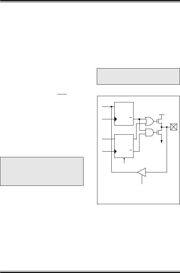
PIC12C67X
5.0I/O PORT
As with any other register, the I/O register can be written and read under program control. However, read instructions (e.g., MOVF GPIO,W) always read the I/O pins independent of the pin’s input/output modes. On RESET, all I/O ports are defined as input (inputs are at hi-impedance) since the I/O control registers are all set.
5.1GPIO
GPIO is an 8-bit I/O register. Only the low order 6 bits are used (GP5:GP0). Bits 7 and 6 are unimplemented and read as '0's.Please note that GP3 is an input only pin. The configuration word can set several I/O’s to alternate functions. When acting as alternate functions the pins will read as ‘0’ during port read. Pins GP0, GP1, and GP3 can be configured with weak pull-ups and also with interrupt on change. The interrupt on change and weak pull-up functions are not pin selectable. If pin 4 is configured as MCLR, the weak pull-up is always on. Interrupt on change for this pin is not set and GP3 will read as '0'Interrupt. on change is enabled by setting INTCON<3>. Note that external oscillator use overrides the GPIO functions on GP4 and GP5.
5.2TRIS Register
This register controls the data direction for GPIO. A '1' from a TRIS register bit puts the corresponding output driver in a hi-impedance mode. A '0' puts the contents of the output data latch on the selected pins, enabling the output buffer. The exceptions are GP3 which is input only and its TRIS bit will always read as '1'.
Note: A read of the ports reads the pins, not the output data latches. That is, if an output driver on a pin is enabled and driven high, but the external system is holding it low, a read of the port will indicate that the pin is low.
Upon reset, the TRIS register is all '1's, making all pins inputs.
5.3I/O Interfacing
The equivalent circuit for an I/O port pin is shown in Figure 5-2. All port pins, except GP3 which is input only, may be used for both input and output operations. For input operations these ports are nonlatching. Any input must be present until read by an input instruction (e.g., MOVF GPIO,W). The outputs are latched and remain unchanged until the output latch is rewritten. To use a port pin as output, the corresponding direction control bit in TRIS must be cleared (= 0). For use as an input, the corresponding TRIS bit must be set. Any I/O pin (except GP3) can be programmed individually as input or output.
Note: On a Power-on Reset, GP0, GP1, GP2, GP4 are configured as analog inputs and read as '0'.
FIGURE 5-1: EQUIVALENT CIRCUIT FOR A SINGLE I/O PIN
Data |
|
|
|
Bus |
D |
Q |
|
|
|
||
WR |
Data |
VDD |
|
Latch |
|
||
|
|
||
Port |
CK |
Q |
|
|
|
||
|
|
P |
|
W |
|
N |
I/O |
Reg |
D |
Q |
pin(1) |
|
|
||
|
TRIS |
VSS |
|
|
Latch |
|
|
TRIS ‘f’ |
|
|
|
CK |
Q |
|
|
|
|
||
|
Reset |
|
|
RD Port
Note 1: I/O pins have protection diodes to VDD and VSS.
GP3 is input only with no data latch and no output drivers.
TABLE 5-1: |
SUMMARY OF PORT REGISTERS |
|
|
|
|
|
|
|
|
|
|
|||||||||
|
|
|
|
|
|
|
|
|
|
|
|
|
|
|
|
|
|
|
||
|
|
|
|
|
|
|
|
|
|
|
|
|
|
|
|
|
Value on |
Value on |
||
|
|
|
|
|
|
|
|
|
|
|
|
|
|
|
|
|
Power-on |
all other |
||
Address |
Name |
|
Bit 7 |
Bit 6 |
Bit 5 |
Bit 4 |
Bit 3 |
Bit 2 |
Bit 1 |
Bit 0 |
Reset |
Resets |
||||||||
|
|
|
|
|
|
|
|
|
|
|
|
|
|
|
|
|
|
|
|
|
85h |
TRIS |
|
|
— |
— |
GPIO Data Direction Register |
|
|
--11 |
1111 |
--11 |
1111 |
||||||||
81h |
OPTION |
|
|
|
INTEDG |
T0CS |
T0SE |
PSA |
PS2 |
PS1 |
PS0 |
1111 |
1111 |
1111 |
1111 |
|||||
GPPU |
||||||||||||||||||||
|
|
|
|
|
|
|
|
|
|
|
|
|
|
|
|
|
|
|
||
03h |
STATUS |
|
IRP(1) |
RP1(1) |
RP0 |
|
|
|
|
|
|
Z |
DC |
C |
0001 |
1xxx |
000q |
quuu |
||
|
TO |
PD |
||||||||||||||||||
05h |
GPIO |
|
|
— |
— |
GP5 |
GP4 |
GP3 |
GP2 |
GP1 |
GP0 |
--xx xxxx |
--uu uuuu |
|||||||
|
|
|
|
|
|
|
|
|
|
|
|
|
|
|
|
|
|
|
|
|
Legend: Shaded cells not used by Port Registers, read as ‘0’, — = unimplemented, read as '0',x = unknown, u = unchanged, q = see tables in Section 7.7 for possible values.
Note 1: The IRP and RP1 bits are reserved on the PIC12C67X, always maintain these bits clear.
1997 Microchip Technology Inc. |
Preliminary |
DS30561A-page 25
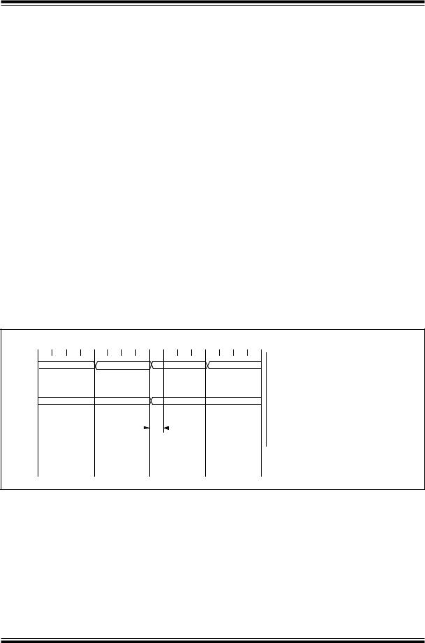
PIC12C67X
5.4I/O Programming Considerations
5.4.1BI-DIRECTIONAL I/O PORTS
Any instruction which writes, operates internally as a read followed by a write operation. The BCF and BSF instructions, for example, read the register into the CPU, execute the bit operation and write the result back to the register. Caution must be used when these instructions are applied to a port with both inputs and outputs defined. For example, a BSF operation on bit5 of GPIO will cause all eight bits of GPIO to be read into the CPU. Then the BSF operation takes place on bit5 and GPIO is written to the output latches. If another bit of GPIO is used as a bi-directional I/O pin (e.g., bit0) and it is defined as an input at this time, the input signal present on the pin itself would be read into the CPU and rewritten to the data latch of this particular pin, overwriting the previous content. As long as the pin stays in the input mode, no problem occurs. However, if bit0 is switched to an output, the content of the data latch may now be unknown.
Reading the port register, reads the values of the port pins. Writing to the port register writes the value to the port latch. When using read-modify-write instructions (ex. BCF, BSF, etc.) on a port, the value of the port pins is read, the desired operation is done to this value, and this value is then written to the port latch.
Example 5-1 shows the effect of two sequential read- modify-write instructions on an I/O port.
EXAMPLE 5-1: READ-MODIFY-WRITE INSTRUCTIONS ON AN I/O PORT
;Initial GPIO Settings
;GPIO<5:3> Inputs
;GPIO<2:0> Outputs
; |
|
GPIO latch |
GPIO pins |
|||
; |
|
---------- |
---------- |
|||
BCF |
GPIO, 5 |
;--01 -ppp |
|
--11 |
pppp |
|
BCF |
GPIO, 4 |
;--10 |
-ppp |
|
--11 |
pppp |
MOVLW |
007h |
; |
|
|
|
|
TRIS |
GPIO |
;--10 |
-ppp |
|
--11 |
pppp |
; |
|
|
|
|
|
|
;Note that the user may have |
expected the pin |
|||||
;values to be --00 pppp. The |
2nd BCF caused |
|||||
;GP5 to be latched as the pin value (High).
A pin actively outputting a Low or High should not be driven from external devices at the same time in order to change the level on this pin (“wired-or”,“wired-and”). The resulting high output currents may damage the chip.
FIGURE 5-2: SUCCESSIVE I/O OPERATION
Q1 Q2 Q3 Q4 Q1 Q2 Q3 Q4 Q1 Q2 Q3 Q4 Q1 Q2 Q3 Q4
Instruction |
PC |
|
PC + 1 |
|
PC + 2 |
PC + 3 |
|
|
|
|
|
|
|
|
|
fetched |
MOVWF GPIO |
MOVF GPIO,W |
|
NOP |
NOP |
||
|
|
||||||
GP5:GP0 |
|
|
|
|
|
|
|
|
|
Port pin |
Port pin |
|
|||
|
|
written here |
sampled here |
|
|||
Instruction |
|
|
|
|
|
|
|
executed |
|
MOVWF GPIO |
MOVF GPIO,W |
NOP |
|||
|
|
||||||
|
|
(Write to |
(Read |
|
|||
|
|
GPIO) |
GPIO) |
|
|||
This example shows a write to GPIO followed by a read from GPIO.
Data setup time = (0.25 TCY – TPD)
where: TCY = instruction cycle.
TPD = propagation delay
Therefore, at higher clock frequencies, a write followed by a read may be problematic.
DS30561A-page 26 |
Preliminary |
1997 Microchip Technology Inc. |
PIC12C67X
6.0TIMER0 MODULE
The Timer0 module timer/counter has the following features:
•8-bit timer/counter
•Readable and writable
•8-bit software programmable prescaler
•Internal or external clock select
•Interrupt on overflow from FFh to 00h
•Edge select for external clock
Figure 6-1 is a simplified block diagram of the Timer0 module.
Timer mode is selected by clearing bit T0CS (OPTION<5>). In timer mode, the Timer0 module will increment every instruction cycle (without prescaler). If the TMR0 register is written, the increment is inhibited for the following two instruction cycles (Figure 6-2 and Figure 6-3). The user can work around this by writing an adjusted value to the TMR0 register.
Counter mode is selected by setting bit T0CS (OPTION<5>). In counter mode, Timer0 will increment either on every rising or falling edge of pin RA4/T0CKI. The incrementing edge is determined by the Timer0 Source Edge Select bit T0SE (OPTION<4>). Clearing
FIGURE 6-1: TIMER0 BLOCK DIAGRAM
bit T0SE selects the rising edge. Restrictions on the external clock input are discussed in detail in Section 6.2.
The prescaler is mutually exclusively shared between the Timer0 module and the Watchdog Timer. The prescaler assignment is controlled in software by control bit PSA (OPTION<3>). Clearing bit PSA will assign the prescaler to the Timer0 module. The prescaler is not readable or writable. When the prescaler is assigned to the Timer0 module, prescale values of 1:2, 1:4, ..., 1:256 are selectable. Section 6.3 details the operation of the prescaler.
6.1Timer0 Interrupt
The TMR0 interrupt is generated when the TMR0 register overflows from FFh to 00h. This overflow sets bit T0IF (INTCON<2>). The interrupt can be masked by clearing bit T0IE (INTCON<5>). Bit T0IF must be cleared in software by the Timer0 module interrupt service routine before re-enabling this interrupt. The TMR0 interrupt cannot awaken the processor from SLEEP since the timer is shut off during SLEEP. See Figure 6- 4 for Timer0 interrupt timing.
|
|
|
|
|
|
|
|
|
|
|
|
|
|
|
|
|
|
|
|
|
|
|
Data bus |
||||
|
|
|
FOSC/4 |
|
|
0 |
|
|
|
|
|
|
1 |
PSout |
|
|
|
|
8 |
|
|
||||||
|
|
|
|
|
|
|
|
|
|
|
|
|
|
|
|
|
|||||||||||
|
|
|
|
|
|
|
|
|
|
|
|
|
|
|
|
|
|
|
|
|
|
|
|||||
|
|
|
|
|
|
|
|
|
|
|
|
|
|
|
|
|
|
|
Sync with |
|
|
|
|
|
|
||
|
|
|
|
|
|
|
|
|
|
|
|
|
|
|
|
|
|
|
|
|
|
|
|
|
|||
|
|
|
|
|
|
|
|
|
|
1 |
|
|
|
|
|
|
|
|
|
|
TMR0 |
|
|
||||
|
|
|
|
|
|
|
|
|
|
|
|
|
|
|
|
|
|
Internal |
|
|
|
||||||
GP2/T0CKI/ |
|
|
|
|
|
|
|
|
|
|
|
Programmable |
|
|
0 |
|
clocks |
|
|
|
|
|
|
||||
|
|
|
|
|
|
|
|
|
|
|
|
|
|
PSout |
|
||||||||||||
|
|
|
|
|
|
|
|
|
|
|
|
|
|
|
|
||||||||||||
AN2 |
|
|
|
|
|
|
|
|
|
|
Prescaler |
|
|
|
|
|
|
|
|
|
|
|
|||||
|
|
|
|
|
|
|
|
|
|
|
|
|
|
(2 cycle delay) |
|
|
|
|
|
|
|||||||
|
|
T0SE |
|
|
|
|
|
|
|
|
|
|
|
|
|
|
|
|
|
|
|
|
|||||
|
|
|
|
|
|
|
|
|
|
|
|
3 |
|
|
|
|
|
|
|
|
|
Set interrupt |
|||||
|
|
|
|
|
|
|
|
|
|
|
|
|
|
|
|
|
|
PSA |
|
|
|
|
|||||
|
|
|
|
|
|
|
|
|
|
|
|
|
PS2, PS1, PS0 |
|
|
||||||||||||
|
|
|
|
|
|
|
|
|
|
|
|
|
|
|
|
|
flag bit T0IF |
||||||||||
|
|
|
|
|
|
|
|
|
|
|
|
|
|||||||||||||||
|
|
|
|
|
|
|
|
T0CS |
|
|
|
|
|
|
|
on overflow |
|||||||||||
Note 1: T0CS, T0SE, PSA, PS2:PS0 (OPTION<5:0>).
2: The prescaler is shared with Watchdog Timer (refer to Figure 6-6 for detailed block diagram).
FIGURE 6-2: TIMER0 TIMING: INTERNAL CLOCK/NO PRESCALE |
|
|
|
|
|
|
|
|
|
|
|
|||||||||||||||||||||
PC |
Q1 |
Q2 |
Q3 |
Q4 |
Q1 |
Q2 |
Q3 |
Q4 |
Q1 |
Q2 |
Q3 |
Q4 |
Q1 |
Q2 |
Q3 |
Q4 |
Q1 |
Q2 |
Q3 |
Q4 |
Q1 |
Q2 |
Q3 |
Q4 |
Q1 |
Q2 |
Q3 |
Q4 |
Q1 |
Q2 |
Q3 |
Q4 |
(Program |
|
|
|
|
|
|
|
|
|
|
|
|
|
|
|
|
|
|
|
|
|
|
|
|
|
|
|
|
|
|
|
|
Counter) |
|
PC-1 |
|
|
PC |
|
|
|
PC+1 |
|
|
PC+2 |
|
|
PC+3 |
|
|
PC+4 |
|
|
PC+5 |
|
|
PC+6 |
|
|||||||
Instruction |
|
|
|
|
MOVWF TMR0 |
MOVF TMR0,W |
MOVF TMR0,W |
MOVF TMR0,W |
MOVF TMR0,W |
MOVF TMR0,W |
|
|
|
|
||||||||||||||||||
Fetch |
|
|
|
|
|
|
|
|
||||||||||||||||||||||||
|
|
|
|
|
|
|
|
|
|
|
|
|
|
|
|
|
|
|
|
|
|
|
|
|
|
|
|
|
|
|
|
|
TMR0 |
T0 |
|
|
|
T0+1 |
|
|
T0+2 |
|
|
NT0 |
|
|
NT0 |
|
|
NT0 |
|
|
|
NT0+1 |
|
|
NT0+2 |
T0 |
|||||||
Instruction |
|
|
|
|
|
|
|
|
|
|
|
|
|
|
|
|
|
|
|
|
|
|
|
|
|
|
|
|
|
|
|
|
Executed |
|
|
|
|
|
|
|
|
Write TMR0 |
Read TMR0 |
Read TMR0 |
Read TMR0 |
Read TMR0 |
Read TMR0 |
||||||||||||||||||
|
|
|
|
|
|
|
|
|
||||||||||||||||||||||||
|
|
|
|
|
|
|
|
|
executed |
|
reads NT0 |
|
reads NT0 |
|
reads NT0 |
|
reads NT0 + 1 |
reads NT0 + 2 |
||||||||||||||
1997 Microchip Technology Inc. |
Preliminary |
DS30561A-page 27

PIC12C67X |
|
|
|
|
|
|
|
|
|
|
|
|
|
|
|
|
|
|
|
|
|
|
|
|
|
|
||||||
FIGURE 6-3: TIMER0 TIMING: INTERNAL CLOCK/PRESCALE 1:2 |
|
|
|
|
|
|
|
|
|
|
||||||||||||||||||||||
PC |
Q1 |
Q2 |
Q3 |
Q4 |
Q1 |
Q2 |
Q3 |
Q4 |
Q1 |
Q2 |
Q3 |
Q4 |
Q1 |
Q2 |
Q3 |
Q4 |
Q1 |
Q2 |
Q3 |
Q4 |
Q1 |
Q2 |
Q3 |
Q4 |
Q1 |
Q2 |
Q3 |
Q4 |
Q1 |
Q2 |
Q3 |
Q4 |
(Program |
|
|
|
|
|
|
|
|
|
|
|
|
|
|
|
|
|
|
|
|
|
|
|
|
|
|
|
|
|
|
|
|
Counter) |
|
PC-1 |
|
|
PC |
|
|
PC+1 |
|
|
PC+2 |
|
|
PC+3 |
|
|
PC+4 |
|
|
PC+5 |
|
|
PC+6 |
|
||||||||
Instruction |
|
|
|
|
MOVWF TMR0 |
MOVF TMR0,W |
MOVF TMR0,W |
MOVF TMR0,W |
MOVF TMR0,W |
MOVF TMR0,W |
|
|
|
|
||||||||||||||||||
Fetch |
|
|
|
|
|
|
|
|
|
|
|
|
|
|
|
|
|
|
|
|
|
|
|
|
|
|
|
|
|
|
|
|
TMR0 |
T0 |
|
|
|
|
|
T0+1 |
|
|
|
|
|
|
|
|
|
|
|
NT0 |
|
|
|
|
|
|
|
|
|
NT0+1 |
|
||
Instruction |
|
|
|
|
|
|
|
|
Write TMR0 |
Read TMR0 |
Read TMR0 |
Read TMR0 |
Read TMR0 |
Read TMR0 |
||||||||||||||||||
Execute |
|
|
|
|
|
|
|
|
||||||||||||||||||||||||
|
|
|
|
|
|
|
|
executed |
|
reads NT0 |
|
reads NT0 |
|
reads NT0 |
|
reads NT0 |
|
reads NT0 + 1 |
||||||||||||||
|
|
|
|
|
|
|
|
|
|
|
|
|
|
|||||||||||||||||||
FIGURE 6-4: |
TIMER0 INTERRUPT TIMING |
|
|
|
|
|
|
|
|
|
|
|
|
|
|
|
|
|
|
|
||||||||||||
Q1 |
Q2 |
Q3 |
Q4 |
Q1 |
Q2 |
Q3 |
Q4 |
Q1 |
Q2 |
Q3 |
Q4 |
Q1 |
Q2 |
Q3 |
Q4 |
Q1 |
Q2 |
Q3 |
Q4 |
OSC1 |
|
|
|
|
|
|
|
|
|
|
|
|
|
|
|
|
|
|
|
CLKOUT(3) |
|
|
|
|
|
|
|
|
|
|
|
|
|
|
|
|
|
|
|
Timer0 |
FEh |
|
|
FFh |
|
|
|
00h |
|
|
01h |
|
|
|
02h |
|
|
||
T0IF bit |
1 |
|
|
|
1 |
|
|
|
|
|
|
|
|
|
|
|
|
|
|
|
|
|
|
|
|
|
|
|
|
|
|
|
|
|
|
|
|
|
|
(INTCON<2>) |
|
|
|
|
|
|
|
|
|
|
|
|
|
|
|
|
|
|
|
GIE bit (INTCON<7>)
INSTRUCTION
FLOW
PC |
|
PC |
PC +1 |
PC +1 |
0004h |
0005h |
Instruction |
|
Inst (PC) |
Inst (PC+1) |
|
Inst (0004h) |
Inst (0005h) |
|
|
|||||
fetched |
|
|
||||
|
|
|||||
Instruction |
|
Inst (PC-1) |
Inst (PC) |
Dummy cycle |
Dummy cycle |
Inst (0004h) |
|
||||||
|
||||||
executed |
|
|||||
|
|
|
|
|
|
|
|
|
|
|
|
|
|
Note 1: Interrupt flag bit T0IF is sampled here (every Q1).
2:Interrupt latency = 4Tcy where Tcy = instruction cycle time.
3:CLKOUT is available only in RC oscillator mode.
DS30561A-page 28 |
Preliminary |
1997 Microchip Technology Inc. |
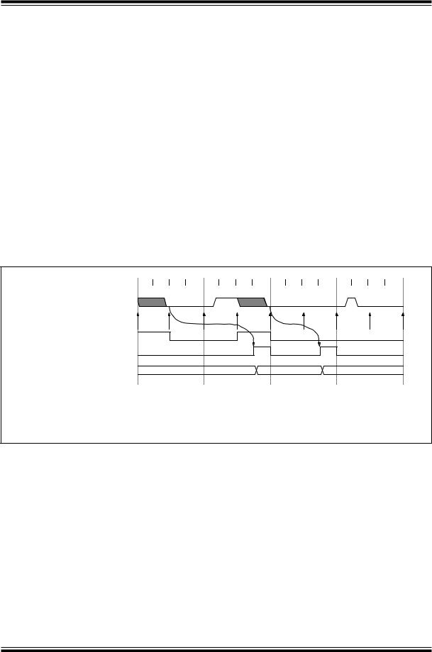
PIC12C67X
6.2Using Timer0 with an External Clock
When an external clock input is used for Timer0, it must meet certain requirements. The requirements ensure the external clock can be synchronized with the internal phase clock (TOSC). Also, there is a delay in the actual incrementing of Timer0 after synchronization.
6.2.1EXTERNAL CLOCK SYNCHRONIZATION
When no prescaler is used, the external clock input is the same as the prescaler output. The synchronization of T0CKI with the internal phase clocks is accomplished by sampling the prescaler output on the Q2 and Q4 cycles of the internal phase clocks (Figure 6-5). Therefore, it is necessary for T0CKI to be high for at least 2Tosc (and a small RC delay of 20 ns) and low for at least 2Tosc (and a small RC delay of 20 ns). Refer to the electrical specification of the desired device.
When a prescaler is used, the external clock input is divided by the asynchronous ripple-counter type pres-
caler so that the prescaler output is symmetrical. For the external clock to meet the sampling requirement, the ripple-counter must be taken into account. Therefore, it is necessary for T0CKI to have a period of at least 4Tosc (and a small RC delay of 40 ns) divided by the prescaler value. The only requirement on T0CKI high and low time is that they do not violate the minimum pulse width requirement of 10 ns. Refer to parameters 40, 41 and 42 in the electrical specification of the desired device.
6.2.2TMR0 INCREMENT DELAY
Since the prescaler output is synchronized with the internal clocks, there is a small delay from the time the external clock edge occurs to the time the Timer0 module is actually incremented. Figure 6-5 shows the delay from the external clock edge to the timer incrementing.
FIGURE 6-5: TIMER0 TIMING WITH EXTERNAL CLOCK
External Clock Input or Prescaler output (2)
External Clock/Prescaler Output after sampling
Increment Timer0 (Q4)
Timer0
Q1 |
Q2 |
Q3 |
Q4 |
Q1 |
Q2 |
Q3 |
Q4 |
Q1 |
Q2 |
Q3 |
Q4 |
Q1 |
Q2 |
Q3 |
Q4 |
|
|
|
|
|
|
|
|
|
|
|
|
|
Small pulse |
||
|
|
|
|
|
|
|
|
|
|
|
|
|
misses sampling |
||
|
|
(1) |
|
|
|
|
|
|
|
|
|
|
|
|
|
(3) |
|
|
|
|
|
|
|
|
|
|
|
|
|
|
|
|
|
|
|
T0 |
|
|
|
T0 + 1 |
|
|
|
T0 + 2 |
|
||
Note 1: Delay from clock input change to Timer0 increment is 3Tosc to 7Tosc. (Duration of Q = Tosc). Therefore, the error in measuring the interval between two edges on Timer0 input = ±4Tosc max.
2:External clock if no prescaler selected, Prescaler output otherwise.
3:The arrows indicate the points in time where sampling occurs.
1997 Microchip Technology Inc. |
Preliminary |
DS30561A-page 29

PIC12C67X
6.3Prescaler
An 8-bit counter is available as a prescaler for the Timer0 module, or as a postscaler for the Watchdog Timer, respectively (Figure 6-6). For simplicity, this counter is being referred to as “prescaler”throughout this data sheet. Note that there is only one prescaler available which is mutually exclusively shared between the Timer0 module and the Watchdog Timer. Thus, a prescaler assignment for the Timer0 module means that there is no prescaler for the Watchdog Timer, and vice-versa.
The PSA and PS2:PS0 bits (OPTION<3:0>) determine the prescaler assignment and prescale ratio.
When assigned to the Timer0 module, all instructions writing to the TMR0 register (e.g. CLRF 1, MOVWF 1, BSF 1,x....etc.) will clear the prescaler. When assigned to WDT, a CLRWDT instruction will clear the prescaler along with the Watchdog Timer. The prescaler is not readable or writable.
FIGURE 6-6: BLOCK DIAGRAM OF THE TIMER0/WDT PRESCALER
CLKOUT (=Fosc/4) |
|
|
|
|
|
|
|
Data Bus |
|
|
|
0 |
M |
1 |
|
|
8 |
|
|
|
|
|
|
|||
GP2/T0CKI/ |
|
|
U |
M |
|
|
||
|
|
|
|
SYNC |
|
|||
AN2 |
|
|
|
X |
|
U |
TMR0 reg |
|
|
|
1 |
0 |
2 |
||||
|
|
|
||||||
|
|
|
|
X |
Cycles |
|
||
|
|
|
|
|
|
|
||
T0SE |
|
|
|
T0CS |
|
|
|
|
|
|
|
|
PSA |
|
Set flag bit T0IF |
||
|
|
|
|
|
|
|||
|
|
|
|
|
|
|
|
on Overflow |
|
0 |
M |
|
8-bit Prescaler |
|
|
|
|
|
|
|
|
|
|
|||
|
|
|
|
|
|
|
|
|
|
1 |
U |
|
|
|
|
|
|
Watchdog |
X |
|
|
8 |
|
|
|
|
|
|
|
|
|
|
|
||
Timer |
|
|
|
|
|
|
|
|
|
|
|
|
8 - to - 1MUX |
|
PS2:PS0 |
|
|
|
|
PSA |
|
|
|
|
|
|
WDT Enable bit |
|
|
|
0 |
1 |
|
|
|
|
|
|
|
|
|
|
|
|
|
|
|
|
|
M U X |
|
PSA |
|
|
|
|
|
|
WDT |
|
|
|
|
|
|
|
|
Time-out |
|
|
|
Note: T0CS, T0SE, PSA, PS2:PS0 are (OPTION<5:0>). |
|
|
|
|||||
DS30561A-page 30 |
Preliminary |
1997 Microchip Technology Inc. |
 Loading...