


PIC16C62A-20I-SP
Microchip Technology Inc PIC16C62A-20I-SP, PIC16C62A-JW, PIC16C62B-JW, PIC16C62A-04-SO, PIC16C62A-04I-SO Datasheet
...
1997 Microchip Technology Inc. DS30234D-page 1
PIC16C6X
8-Bit CMOS Microcontrollers
Devices included in this data sheet:
PIC16C6X Microcontroller Core Features:
• High performance RISC CPU
• Only 35 single word instructions to learn
• All single cycle instructions except for program
branches which are two-cycle
• Operating speed: DC - 20 MHz clock input
DC - 200 ns instruction cycle
• Interrupt capability
• Eight level deep hardware stack
• Direct, indirect, and relative addressing modes
• Power-on Reset (POR)
• Power-up Timer (PWRT) and
Oscillator Start-up Timer (OST)
• Watchdog Timer (WDT) with its own on-chip RC
oscillator for reliable operation
• Programmable code-protection
• Power saving SLEEP mode
• Selectable oscillator options
• PIC16C61 • PIC16C64A
• PIC16C62 • PIC16CR64
• PIC16C62A • PIC16C65
• PIC16CR62 • PIC16C65A
• PIC16C63 • PIC16CR65
• PIC16CR63 • PIC16C66
• PIC16C64 • PIC16C67
• Low-power, high-speed CMOS EPROM/ROM
technology
• Fully static design
• Wide operating voltage range: 2.5V to 6.0V
• Commercial, Industrial, and Extended
temperature ranges
• Low-power consumption:
•
< 2 mA @ 5V, 4 MHz
•
15
µ
A typical @ 3V, 32 kHz
•
< 1
µ
A typical standby current
PIC16C6X Peripheral Features:
• Timer0: 8-bit timer/counter with 8-bit prescaler
• Timer1: 16-bit timer/counter with prescaler,
can be incremented during sleep via
external crystal/clock
• Timer2: 8-bit timer/counter with 8-bit period
register, prescaler and postscaler
• Capture/Compare/PWM (CCP) module(s)
• Capture is 16-bit, max resolution is 12.5 ns,
Compare is 16-bit, max resolution is 200 ns,
PWM max resolution is 10-bit.
• Synchronous Serial Port (SSP) with SPI
and I
2
C
• Universal Synchronous Asynchronous Receiver
Transmitter (USART/SCI)
• Parallel Slave Port (PSP) 8-bits wide, with
external RD
, WR and CS controls
• Brown-out detection circuitry for
Brown-out Reset (BOR)
PIC16C6X Features 61 62 62A R62 63 R63 64 64A R64 65 65A R65 66 67
Program Memory
(EPROM) x 14
1K 2K 2K — 4K — 2K 2K — 4K 4K — 8K 8K
(ROM) x 14 — — — 2K — 4K — — 2K — — 4K — —
Data Memory (Bytes) x 8 36 128 128 128 192 192 128 128 128 192 192 192 368 368
I/O Pins 13 22 22 22 22 22 33 33 33 33 33 33 22 33
Parallel Slave Port ———— — —YesYesYesYes Yes Yes — Yes
Capture/Compare/PWM
Module(s)
—1112211122222
Timer Modules 1333 3 3 333 33333
Serial Communication
— SPI/
I
2
C
SPI/
I
2
C
SPI/
I
2
C
SPI/I
2
C,
USART
SPI/I
2
C,
USART
SPI/
I
2
C
SPI/
I
2
C
SPI/
I
2
C
SPI/I
2
C,
USART
SPI/I
2
C,
USART
SPI/I
2
C,
USART
SPI/I
2
C,
USART
SPI/I
2
C,
USART
In-Circuit Serial
Programming
Yes Yes Yes Yes Yes Yes Yes Yes Yes Yes Yes Yes Yes Ye s
Brown-out Reset — — Yes Yes Yes Yes — Yes Yes — Yes Yes Yes Yes
Interrupt Sources 377710 10 888 11 11 11 10 11
Sink/Source Current (mA) 25/20 25/25 25/25 25/25 25/25 25/25 25/25 25/25 25/25 25/25 25/25 25/25 25/25 25/25

PIC16C6X
DS30234D-page 2
1997 Microchip Technology Inc.
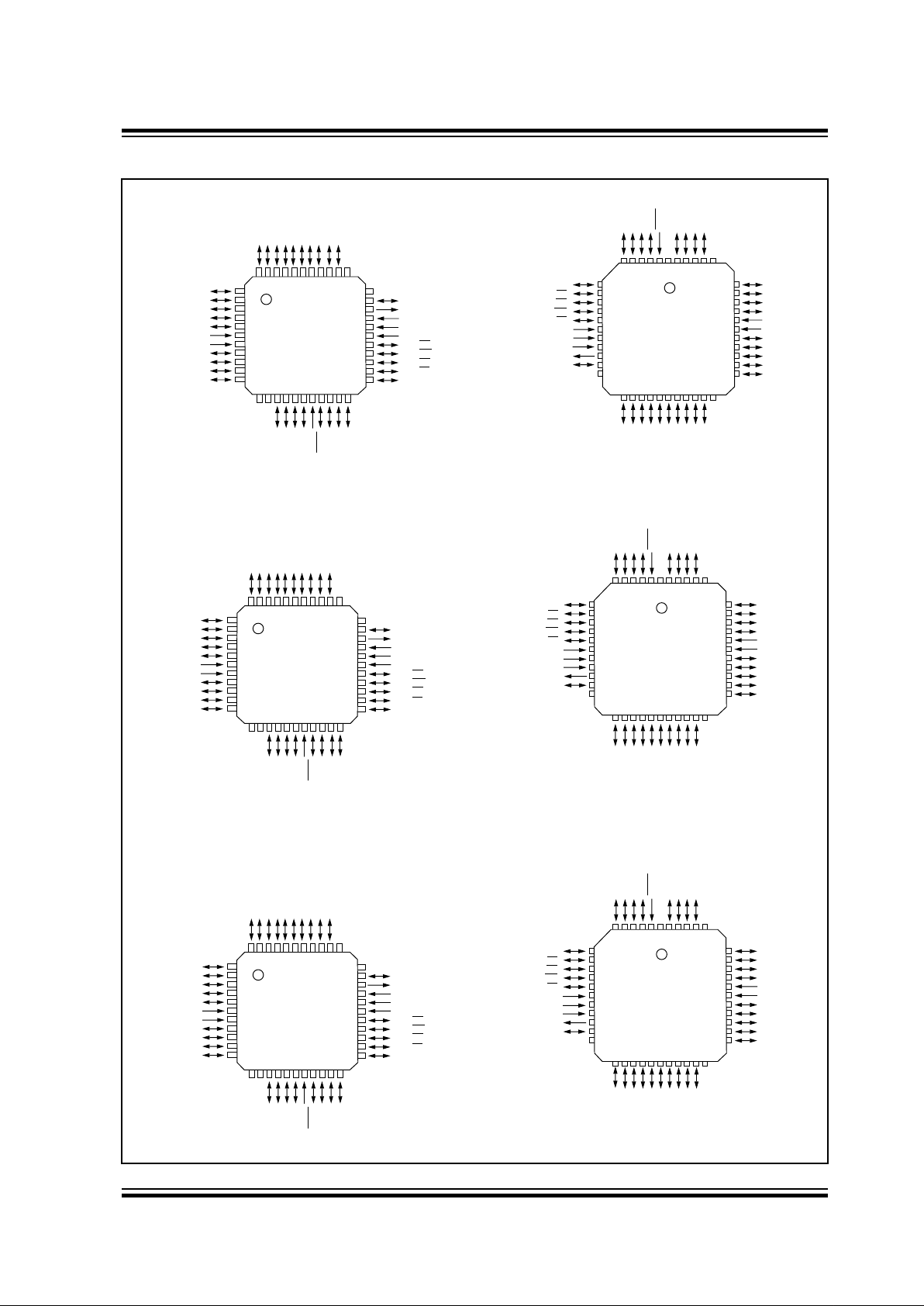
Pin Diagrams
PDIP, SOIC, Windowed CERDIP
18
17
16
15
14
13
12
11
10
1
2
3
4
5
6
7
8
9
PIC16C61
RB7
RB6
RB5
RB4
RB3
RB2
RB1
RB0/INT
VDD
VSS
RC7
RC6
RC5/SDO
RC4/SDI/SDA
MCLR/VPP
RA0
RA1
RA2
RA3
RA4/T0CKI
RA5/SS
VSS
OSC1/CLKIN
OSC2/CLKOUT
RC0/T1OSI/T1CKI
RC1/T1OSO
1
2
3
4
5
6
7
8
9
10
11
12
13
14
28
27
26
25
24
23
22
21
20
19
18
17
16
15
PIC16C62
RC2/CCP1
RC3/SCK/SCL
SDIP, SOIC, SSOP, Windowed CERDIP (300 mil)
RA2
RA3
RA4/T0CKI
MCLR/VPP
VSS
RB0/INT
RB1
RB2
RB3
RA1
RA0
OSC1/CLKIN
OSC2/CLKOUT
VDD
RB7
RB6
RB5
RB4
RB7
RB6
RB5
RB4
RB3
RB2
RB1
RB0/INT
V
DD
VSS
RC7/RX/DT
RC6/TX/CK
RC5/SDO
RC4/SDI/SDA
MCLR/VPP
RA0
RA1
RA2
RA3
RA4/T0CKI
RA5/SS
VSS
OSC1/CLKIN
OSC2/CLKOUT
RC0/T1OSO/T1CKI
RC1/T1OSI/CCP2
1
2
3
4
5
6
7
8
9
10
11
12
13
14
28
27
26
25
24
23
22
21
20
19
18
17
16
15
PIC16C63
RC2/CCP1
RC3/SCK/SCL
SDIP, SOIC, Windowed CERDIP (300 mil)
RB7
RB6
RB5
RB4
RB3
RB2
RB1
RB0/INT
V
DD
VSS
RC7
RC6
RC5/SDO
RC4/SDI/SDA
MCLR/VPP
RA0
RA1
RA2
RA3
RA4/T0CKI
RA5/SS
VSS
OSC1/CLKIN
OSC2/CLKOUT
RC0/T1OSO/T1CKI
RC1/T1OSI
1
2
3
4
5
6
7
8
9
10
11
12
13
14
28
27
26
25
24
23
22
21
20
19
18
17
16
15
PIC16C62A
RC2/CCP1
RC3/SCK/SCL
SDIP, SOIC, SSOP, Windowed CERDIP (300 mil)
PIC16CR62
RB7
RB6
RB5
RB4
RB3
RB2
RB1
RB0/INT
V
DD
VSS
RD7/PSP7
RD6/PSP6
RD5/PSP5
RD4/PSP4
RC7/RX/DT
RC6/TX/CK
RC5/SDO
RC4/SDI/SDA
RD3/PSP3
RD2/PSP2
MCLR/VPP
RA0
RA1
RA2
RA3
RA4/T0CKI
RA5/SS
RE0/RD
RE1/WR
RE2/CS
VDD
VSS
OSC1/CLKIN
OSC2/CLKOUT
RC0/T1OSO/T1CKI
RC1/T1OSI/CCP2
RC2/CCP1
RC3/SCK/SCL
RD0/PSP0
RD1/PSP1
1
2
3
4
5
6
7
8
9
10
11
12
13
14
15
16
17
18
19
20
40
39
38
37
36
35
34
33
32
31
30
29
28
27
26
25
24
23
22
21
PIC16C65
PDIP , Windowed CERDIP
RB7
RB6
RB5
RB4
RB3
RB2
RB1
RB0/INT
V
DD
VSS
RD7/PSP7
RD6/PSP6
RD5/PSP5
RD4/PSP4
RC7
RC6
RC5/SDO
RC4/SDI/SDA
RD3/PSP3
RD2/PSP2
MCLR/VPP
RA0
RA1
RA2
RA3
RA4/T0CKI
RA5/SS
RE0/RD
RE1/WR
RE2/CS
VDD
VSS
OSC1/CLKIN
OSC2/CLKOUT
RC0/T1OSI/T1CKI
RC1/T1OSO
RC2/CCP1
RC3/SCK/SCL
RD0/PSP0
RD1/PSP1
1
2
3
4
5
6
7
8
9
10
11
12
13
14
15
16
17
18
19
20
40
39
38
37
36
35
34
33
32
31
30
29
28
27
26
25
24
23
22
21
PIC16C64
RB7
RB6
RB5
RB4
RB3
RB2
RB1
RB0/INT
V
DD
VSS
RD7/PSP7
RD6/PSP6
RD5/PSP5
RD4/PSP4
RC7
RC6
RC5/SDO
RC4/SDI/SDA
RD3/PSP3
RD2/PSP2
MCLR/VPP
RA0
RA1
RA2
RA3
RA4/T0CKI
RA5/SS
RE0/RD
RE1/WR
RE2/CS
VDD
VSS
OSC1/CLKIN
OSC2/CLKOUT
RC0/T1OSO/T1CKI
RC1/T1OSI
RC2/CCP1
RC3/SCK/SCL
RD0/PSP0
RD1/PSP1
1
2
3
4
5
6
7
8
9
10
11
12
13
14
15
16
17
18
19
20
40
39
38
37
36
35
34
33
32
31
30
29
28
27
26
25
24
23
22
21
PIC16C64A
PIC16C65A
PIC16CR64
PIC16CR63
PIC16CR65
PIC16C66
PIC16C67
1997 Microchip Technology Inc. DS30234D-page 3
PIC16C6X
Pin Diagrams (Cont.’d)
NC
RC0/T1OSO/T1CKI
OSC2/CLKOUT
OSC1/CLKIN
V
SS
VDD
RE2/CS
RE1/WR
RE0/RD
RA5/SS
RA4/T0CKI
RC7/RX/DT
RD4/PSP4
RD5/PSP5
RD6/PSP6
RD7/PSP7
V
SS
VDD
RB0/INT
RB1
RB2
RB3
RC6/TX/CK
RC5/SDO
RC4/SDI/SDA
RD3/PSP3
RD2/PSP2
RD1/PSP1
RD0/PSP0
RC3/SCK/SCL
RC2/CCP1
RC1/T1OSI/CCP2
NC
1
2
3
4
5
6
7
8
9
10
11
33
32
31
30
29
28
27
26
25
24
23
RA3
RA2
RA1
RA0
MCLR/VPP
RB7
RB6
RB5
RB4
NC
NC
44
43
42
41
40
39
38
37
36
35
34
22
21
20
19
18
17
16
15
14
13
12
PIC16C65
MQFP,
RB3
RB2
RB1
RB0/INT
V
DD
VSS
RD7/PSP7
RD6/PSP6
RD5/PSP5
RD4/PSP4
RC7/RX/DT
RA4/T0CKI
RA5/SS
RE0/RD
RE1/WR
RE2/CS
VDD
VSS
OSC1/CLKIN
OSC2/CLKOUT
NC
RA3
RA2
RA1
RA0
MCLR/VPP
NC
RB7
RB6
RB5
RB4
NC
7
8
9
10
11
12
13
14
15
16
17
39
38
37
36
35
34
33
32
31
30
29
NC
RC6/TX/CK
RC5/SDO
RC4/SDI/SDA
RD3/PSP3
RD2/PSP2
RD1/PSP1
RD0/PSP0
RC3/SCK/SCL
RC2/CCP1
RC1/T1OSI
6
5
4
3
2
1
44
43
42
41
40
28
27
26
25
24
23
22
21
20
19
18
PIC16C65
/CCP2
PLCC
RC0/T1OSO/T1CKI
NC
RC0/T1OSO/T1CKI
OSC2/CLKOUT
OSC1/CLKIN
V
SS
VDD
RE2/CS
RE1/WR
RE0/RD
RA5/SS
RA4/T0CKI
RC7
RD4/PSP4
RD5/PSP5
RD6/PSP6
RD7/PSP7
V
SS
VDD
RB0/INT
RB1
RB2
RB3
RC6
RC5/SDO
RC4/SDI/SDA
RD3/PSP3
RD2/PSP2
RD1/PSP1
RD0/PSP0
RC3/SCK/SCL
RC2/CCP1
RC1/T1OSI
NC
1
2
3
4
5
6
7
8
9
10
11
33
32
31
30
29
28
27
26
25
24
23
RA3
RA2
RA1
RA0
MCLR
/VPP
RB7
RB6
RB5
RB4
NC
NC
34
35
36
37
38
39
40
41
42
43
44
PIC16C64A
MQFP,
RB3
RB2
RB1
RB0/INT
V
DD
VSS
RD7/PSP7
RD6/PSP6
RD5/PSP5
RD4/PSP4
RC7
RA4/T0CKI
RA5/SS
RE0/RD
RE1/WR
RE2/CS
VDD
VSS
OSC1/CLKIN
OSC2/CLKOUT
NC
RA3
RA2
RA1
RA0
MCLR/VPP
NC
RB7
RB6
RB5
RB4
NC
7
8
9
10
11
12
13
14
15
16
17
39
38
37
36
35
34
33
32
31
30
29
NC
RC6
RC5/SDO
RC4/SDI/SDA
RD3/PSP3
RD2/PSP2
RD1/PSP1
RD0/PSP0
RC3/SCK/SCL
RC2/CCP1
RC1/T1OSI
6
5
4
3
2
1
44
43
42
41
40
28
27
26
25
24
23
22
21
20
19
18
PIC16C64A
PLCC
RC0/T1OSO/T1CKI
PIC16CR64
PIC16CR64
PIC16C65A
PIC16C65A
TQFP (PIC16C64A only)
TQFP (Not on PIC16C65)
RB3
RB2
RB1
RB0/INT
V
DD
VSS
RD7/PSP7
RD6/PSP6
RD5/PSP5
RD4/PSP4
RC7
RA4/T0CKI
RA5/SS
RE0/RD
RE1/WR
RE2/CS
VDD
VSS
OSC1/CLKIN
NC
RA3
RA2
RA1
RA0
MCLR/VPP
NC
RB7
RB6
RB5
RB4
NC
7
8
9
10
11
12
13
14
15
16
17
39
38
37
36
35
34
33
32
31
30
29
NC
RC6
RC5/SDO
RC4/SDI/SDA
RD3/PSP3
RD2/PSP2
RD1/PSP1
RD0/PSP0
RC3/SCK/SCL
RC2/CCP1
RC1/T1OSO
6
5
4
3
2
1
44
43
42
41
40
28
27
26
25
24
23
22
21
20
19
18
PIC16C64
PLCC
NC
RC0/T1OSI/T1CKI
OSC2/CLKOUT
OSC1/CLKIN
V
SS
VDD
RE2/CS
RE1/WR
RE0/RD
RA5/SS
RA4/T0CKI
RC7
RD4/PSP4
RD5/PSP5
RD6/PSP6
RD7/PSP7
V
SS
VDD
RB0/INT
RB1
RB2
RB3
RC6
RC5/SDO
RC4/SDI/SDA
RD3/PSP3
RD2/PSP2
RD1/PSP1
RD0/PSP0
RC3/SCK/SCL
RC2/CCP1
RC1/T1OSO
NC
1
2
3
4
5
6
7
8
9
10
11
33
32
31
30
29
28
27
26
25
24
23
RA3
RA2
RA1
RA0
MCLR
/VPP
RB7
RB6
RB5
RB4
NC
NC
44
43
42
41
40
39
38
37
36
35
34
22
21
20
19
18
17
16
15
14
13
12
PIC16C64
MQFP
RC0/T1OSI/T1CKI
OSC2/CLKOUT
22
21
20
19
18
17
16
15
14
13
12
PIC16CR65
PIC16CR65
PIC16C67
PIC16C67

PIC16C6X
DS30234D-page 4
1997 Microchip Technology Inc.
Table Of Contents
1.0 General Description....................................................................................................................................................................... 5
2.0 PIC16C6X Device Varieties........................................................................................................................................................... 7
3.0 Architectural Overview................................................................................................................................................................... 9
4.0 Memory Organization................................................................................................................................................................... 19
5.0 I/O Ports....................................................................................................................................................................................... 51
6.0 Overview of Timer Modules......................................................................................................................................................... 63
7.0 Timer0 Module............................................................................................................................................................................. 65
8.0 Timer1 Module............................................................................................................................................................................. 71
9.0 Timer2 Module............................................................................................................................................................................. 75
10.0 Capture/Compare/PWM (CCP) Module(s)................................................................................................................................... 77
11.0 Synchronous Serial Port (SSP) Module....................................................................................................................................... 83
12.0 Universal Synchronous Asynchronous Receiver Transmitter (USART) Module ....................................................................... 105
13.0 Special Features of the CPU ..................................................................................................................................................... 123
14.0 Instruction Set Summary............................................................................................................................................................ 143
15.0 Development Support ................................................................................................................................................................ 159
16.0 Electrical Characteristics for PIC16C61..................................................................................................................................... 163
17.0 DC and AC Characteristics Graphs and Tables for PIC16C61.................................................................................................. 173
18.0 Electrical Characteristics for PIC16C62/64................................................................................................................................ 183
19.0 Electrical Characteristics for PIC16C62A/R62/64A/R64............................................................................................................ 199
20.0 Electrical Characteristics for PIC16C65..................................................................................................................................... 215
21.0 Electrical Characteristics for PIC16C63/65A ............................................................................................................................. 231
22.0 Electrical Characteristics for PIC16CR63/R65........................................................................................................................... 247
23.0 Electrical Characteristics for PIC16C66/67................................................................................................................................ 263
24.0 DC and AC Characteristics Graphs and Tables for:
PIC16C62, PIC16C62A, PIC16CR62, PIC16C63, PIC16C64, PIC16C64A, PIC16CR64,
PIC16C65A, PIC16C66, PIC16C67........................................................................................................................................... 281
25.0 Packaging Information ............................................................................................................................................................... 291
Appendix A: Modifications.............................................................................................................................................................. 307
Appendix B: Compatibility.............................................................................................................................................................. 307
Appendix C: What’s New................................................................................................................................................................ 308
Appendix D: What’s Changed ........................................................................................................................................................ 308
Appendix E: PIC16/17 Microcontrollers....................................................................................................................................... 309
Pin Compatibility ................................................................................................................................................................................ 315
Index .................................................................................................................................................................................................. 317
List of Equation and Examples........................................................................................................................................................... 326
List of Figures..................................................................................................................................................................................... 326
List of Tables...................................................................................................................................................................................... 330
Reader Response.............................................................................................................................................................................. 334
PIC16C6X Product Identification System........................................................................................................................................... 335
For register and module descriptions in this data sheet, device legends show which de vices apply to those sections . For
example, the legend below shows that some features of only the PIC16C62A, PIC16CR62, PIC16C63, PIC16C64A,
PIC16CR64, and PIC16C65A are described in this section.
Applicable Devices
61
62 62A R62 63 R63 64 64A R64 65 65A R65 66 67
To Our Valued Customers
We constantly strive to improve the quality of all our products and documentation. We have spent an exceptional
amount of time to ensure that these documents are correct. However, we realize that we may have missed a few
things. If you find any information that is missing or appears in error, please use the reader response for m in the
back of this data sheet to inform us. We appreciate your assistance in making this a better document.

1997 Microchip Technology Inc. DS30234D-page 5
PIC16C6X
1.0 GENERAL DESCRIPTION
The PIC16CXX is a family of
low-cost, high-perfor-
mance, CMOS, fully-static, 8-bit microcontrollers.
All PIC16/17 microcontrollers employ an advanced
RISC architecture. The PIC16CXX microcontroller fam-
ily has enhanced core features, eight-level deep stack,
and multiple internal and external interrupt sources.
The separate instruction and data buses of the Harvard
architecture allow a 14-bit wide instruction word with
separate 8-bit wide data. The two stage instruction
pipeline allows all instructions to execute in a single
cycle, except for program branches (which require two
cycles). A total of 35 instructions (reduced instruction
set) are available . Additionally, a large register set gives
some of the architectural innovations used to achie v e a
very high performance.
PIC16CXX microcontrollers typically achieve a 2:1
code compression and a 4:1 speed improvement over
other 8-bit microcontrollers in their class.
The
PIC16C61
device has 36 bytes of RAM and 13 I/O
pins. In addition a timer/counter is available.
The
PIC16C62/62A/R62
devices have 128 bytes of
RAM and 22 I/O pins. In addition, several peripheral
features are available, including: three timer/counters,
one Capture/Compare/PWM module and one serial
port. The Synchronous Serial Por t can be configured
as either a 3-wire Serial Peripheral Interface (SPI
) or
the two-wire Inter-Integrated Circuit (I
2
C) bus.
The
PIC16C63/R63
devices have 192 bytes of RAM,
while the
PIC16C66
has 368 bytes. All three devices
have 22 I/O pins. In addition, several peripheral fea-
tures are available, including: three timer/counters, two
Capture/Compare/PWM modules and two serial ports.
The Synchronous Serial Port can be configured as
either a 3-wire Serial Peripheral Interface (SPI) or the
two-wire Inter-Integrated Circuit (I
2
C) bus. The Univer-
sal Synchronous Asynchronous Receiver Transmitter
(USART) is also know as a Serial Communications
Interface or SCI.
The
PIC16C64/64A/R64
devices have 128 bytes of
RAM and 33 I/O pins. In addition, several peripheral
features are available, including: three timer/counters,
one Capture/Compare/PWM module and one serial
port. The Synchronous Serial Por t can be configured
as either a 3-wire Serial Peripheral Interface (SPI) or
the two-wire Inter-Integrated Circuit (I
2
C) bus. An 8-bit
Parallel Slave Port is also provided.
The
PIC16C65/65A/R65
devices have 192 bytes of
RAM, while the
PIC16C67
has 368 bytes. All four
devices have 33 I/O pins. In addition, se ver al peripheral
features are available, including: three timer/counters,
two Capture/Compare/PWM modules and two serial
ports. The Synchronous Serial Port can be configured
as either a 3-wire Serial Peripheral Interface (SPI) or
the two-wire Inter-Integrated Circuit (I
2
C) bus. The Uni-
versal Synchronous Asynchronous Receiver Transmit-
ter (USART) is also known as a Serial Communications
Interface or SCI. An 8-bit P arallel Sla ve Port is also pro-
vided.
The PIC16C6X device family has special features to
reduce external components, thus reducing cost,
enhancing system reliability and reducing power con-
sumption. There are f our oscillator options , of which the
single pin RC oscillator provides a low-cost solution,
the LP oscillator minimizes power consumption, XT is a
standard crystal, and the HS is for High Speed crystals.
The SLEEP (power-down) mode offers a power saving
mode. The user can wake the chip from SLEEP
through several external and internal interrupts, and
resets.
A highly reliable Watchdog Timer with its own on-chip
RC oscillator provides protection against software lock-
up.
A UV erasable CERDIP packaged version is ideal for
code development, while the cost-effective
One-Time-Programmable (OTP) version is suitable for
production in any volume.
The PIC16C6X family fits perfectly in applications rang-
ing from high-speed automotive and appliance control
to low-power remote sensors, keyboards and telecom
processors. The EPROM technology makes customi-
zation of application programs (transmitter codes,
motor speeds, receiver frequencies, etc.) extremely
fast and convenient. The small footprint packages
make this microcontroller series perfect for all applica-
tions with space limitations. Low-cost, low-power, high
performance, ease-of-use, and I/O flexibility make the
PIC16C6X very versatile even in areas where no micro-
controller use has been considered before (e.g. timer
functions, serial communication, capture and compare,
PWM functions, and co-processor applications).
1.1 F
amily and Upward Compatibility
Those users familiar with the PIC16C5X family of
microcontrollers will realize that this is an enhanced
version of the PIC16C5X architecture. Please refer to
Appendix A for a detailed list of enhancements. Code
written for PIC16C5X can be easily ported to
PIC16CXX family of devices (Appendix B).
1.2 De
velopment Support
PIC16C6X devices are supported by the complete line
of Microchip Development tools.
Please refer to Section 15.0 for more details about
Microchip’s development tools.
PIC16C6X
DS30234D-page 6
1997 Microchip Technology Inc.
TABLE 1-1: PIC16C6X FAMILY OF DEVICES
PIC16C61
PIC16C62A PIC16CR62 PIC16C63 PIC16CR63
Clock
Maximum Frequency
of Operation (MHz)
20 20 20 20 20
Memory
EPROM Program Memory
(x14 words)
1K 2K — 4K —
ROM Program Memory
(x14 words)
— — 2K — 4K
Data Memory (bytes) 36 128 128 192 192
Peripherals
Timer Module(s) TMR0 TMR0,
TMR1,
TMR2
TMR0,
TMR1,
TMR2
TMR0,
TMR1,
TMR2
TMR0,
TMR1,
TMR2
Capture/Compare/
PWM Module(s)
—1122
Serial Port(s)
(SPI/I
2
C, USART)
— SPI/I
2
C SPI/I
2
C SPI/I
2
C,
USART
SPI/I
2
C
USART
Parallel Slave Port — — — — —
Features
Interrupt Sources 3 7 7 10 10
I/O Pins 13 22 22 22 22
Voltage Range (Volts) 3.0-6.0 2.5-6.0 2.5-6.0 2.5-6.0 2.5-6.0
In-Circuit Serial Programming Yes Yes Yes Yes Yes
Brown-out Reset — Yes Yes Yes Yes
Packages 18-pin DIP, SO 28-pin SDIP,
SOIC, SSOP
28-pin SDIP,
SOIC, SSOP
28-pin SDIP,
SOIC
28-pin SDIP,
SOIC
PIC16C64A
PIC16CR64 PIC16C65A PIC16CR65 PIC16C66 PIC16C67
Clock
Maximum Frequency
of Operation (MHz)
20 20 20 20 20 20
Memory
EPROM Program Memory
(x14 words)
2K — 4K — 8K 8K
ROM Program Memory (x14
words)
—2K— 4K——
Data Memory (bytes) 128 128 192 192 368 368
Peripherals
Timer Module(s) TMR0,
TMR1,
TMR2
TMR0,
TMR1,
TMR2
TMR0,
TMR1,
TMR2
TMR0,
TMR1,
TMR2
TMR0,
TMR1,
TMR2
TMR0,
TMR1,
TMR2
Capture/Compare/PWM Mod-
ule(s)
1 1 2 222
Serial Port(s) (SPI/I
2
C, USART) SPI/I
2
C SPI/I
2
C SPI/I
2
C,
USART
SPI/I
2
C,
USART
SPI/I
2
C,
USART
SPI/I
2
C,
USART
Parallel Slave Port Yes Yes Yes Yes — Yes
Features
Interrupt Sources 8 8 11 11 10 11
I/O Pins 33 33 33 33 22 33
Voltage Range (Volts) 2.5-6.0 2.5-6.0 2.5-6.0 2.5-6.0 2.5-6.0 2.5-6.0
In-Circuit Serial Programming Yes Yes Yes Yes Yes Yes
Brown-out Reset Yes Yes Yes Yes Yes Yes
Packages 40-pin DIP;
44-pin PLCC,
MQFP, TQFP
40-pin DIP;
44-pin PLCC,
MQFP, TQFP
40-pin DIP;
44-pin PLCC,
MQFP, TQFP
40-pin DIP;
44-pin
PLCC,
MQFP,
TQFP
28-pin SDIP,
SOIC
40-pin DIP;
44-pin
PLCC,
MQFP,
TQFP
All PIC16/17 Family devices have Power-on Reset, selectable Watchdog Timer, selectable code protect and high I/O current
capability. All PIC16C6X Family devices use serial programming with clock pin RB6 and data pin RB7.

1997 Microchip Technology Inc. DS30234D-page 7
PIC16C6X
2.0 PIC16C6X DEVICE VARIETIES
A variety of frequency ranges and packaging options
are available . Depending on application and production
requirements, the proper device option can be selected
using the information in the PIC16C6X Product Identifi-
cation System section at the end of this data sheet.
When placing orders, please use that page of the data
sheet to specify the correct part number.
For the PIC16C6X family of devices, there are four
device “types” as indicated in the device number:
1. C, as in PIC16C64. These devices have
EPROM type memory and operate over the
standard voltage range.
2. LC, as in PIC16LC64. These devices have
EPROM type memory and operate over an
extended voltage range.
3. CR, as in PIC16CR64. These devices have
ROM program memory and operate over the
standard voltage range.
4. LCR, as in PIC16LCR64. These devices have
ROM program memory and operate over an
extended voltage range.
2.1 UV Erasable Devices
The UV erasable version, offered in CERDIP package
is optimal for prototype development and pilot
programs. This version can be erased and
reprogrammed to any of the oscillator modes.
Microchip's PICSTART
Plus and PRO MATE
II
programmers both support programming of the
PIC16C6X.
2.2 One-Time-Programmable (OTP)
Devices
The availability of OTP devices is especially useful for
customers who need the flexibility for frequent code
updates and small volume applications.
The OTP devices, packaged in plastic packages, per-
mit the user to program them once. In addition to the
program memory, the configuration bits must also be
programmed.
2.3 Quick-Turnaround-Production (QTP)
Devices
Microchip offers a QTP Programming Service for fac-
tory production orders. This service is made available
for users who choose not to program a medium to high
quantity of units and whose code patterns have stabi-
lized. The devices are identical to the OTP devices but
with all EPROM locations and configuration options
already programmed by the factory. Certain code and
prototype verification procedures apply before produc-
tion shipments are available. Please contact your local
Microchip Technology sales office for more details.
2.4 Serialized Quick-Turnaround
Production (SQTP
SM
) Devices
Microchip offers a unique programming service where
a few user-defined locations in each device are pro-
grammed with different serial numbers. The serial num-
bers may be random, pseudo-random, or sequential.
Serial programming allows each device to have a
unique number which can serve as an entry-code,
password, or ID number.
ROM devices do not allow serialization information in
the program memory space. The user may have this
information programmed in the data memory space.
For information on submitting ROM code, please con-
tact your regional sales office.
2.5 Read Only Memory (ROM) Devices
Microchip offers masked ROM versions of several of
the highest volume parts, thus giving customers a low
cost option for high volume, mature products.
For information on submitting ROM code, please con-
tact your regional sales office.

PIC16C6X
DS30234D-page 8 1997 Microchip Technology Inc.
NOTES:

1997 Microchip Technology Inc. DS30234D-page 9
PIC16C6X
3.0 ARCHITECTURAL OVERVIEW
The high performance of the PIC16CXX family can be
attributed to a number of architectural features com-
monly found in RISC microprocessors. To begin with,
the PIC16CXX uses a Harvard architecture, in which,
program and data are accessed from separate memo-
ries using separate buses. This improves bandwidth
over traditional von Neumann architecture where pro-
gram and data may be fetched from the same memory
using the same bus. Separ ating program and data b us-
ses further allows instructions to be sized differently
than 8-bit wide data words. Instruction opcodes are
14-bits wide making it possible to have all single word
instructions. A 14-bit wide program memory access
bus fetches a 14-bit instruction in a single cycle. A two-
stage pipeline overlaps fetch and execution of instruc-
tions (Example 3-1). Consequently, all instructions exe-
cute in a single cycle (200 ns @ 20 MHz) except for
program branches.
The PIC16C61 addresses 1K x 14 of program memory.
The PIC16C62/62A/R62/64/64A/R64 address 2K x 14 of
program memory, and the PIC16C63/R63/65/65A/R65
devices address 4K x 14 of program memory. The
PIC16C66/67 address 8K x 14 program memory. All
program memory is internal.
The PIC16CXX can directly or indirectly address its
register files or data memory. All special function reg-
isters including the program counter are mapped in
the data memory. The PIC16CXX has an orthogonal
(symmetrical) instruction set that makes it possible to
carry out any operation on any register using any
addressing mode. This symmetrical nature and lack of
“special optimal situations” makes programming with
the PIC16CXX simple yet efficient, thus significantly
reducing the learning curve.
The PIC16CXX device contains an 8-bit ALU and work-
ing register (W). The ALU is a general pur pose arith-
metic unit. It perf orms arithmetic and Boolean functions
between data in the working register and any register
file.
The ALU is 8-bits wide and capable of addition, sub-
traction, shift, and logical operations. Unless otherwise
mentioned, arithmetic operations are two's comple-
ment in nature. In two-operand instructions, typically
one operand is the working register (W register), the
other operand is a file register or an immediate con-
stant. In single operand instructions, the operand is
either the W register or a file register.
The W register is an 8-bit working register used for ALU
operations. It is not an addressable register.
Depending upon the instruction executed, the ALU may
affect the values of the Carry (C), Digit Carry (DC), and
Zero (Z) bits in the STATUS register. Bits C and DC
operate as a borro
w and digit borrow out bit, respec-
tively, in subtraction. See the SUBLW and SUBWF
instructions for examples.
PIC16C6X
DS30234D-page 10 1997 Microchip Technology Inc.
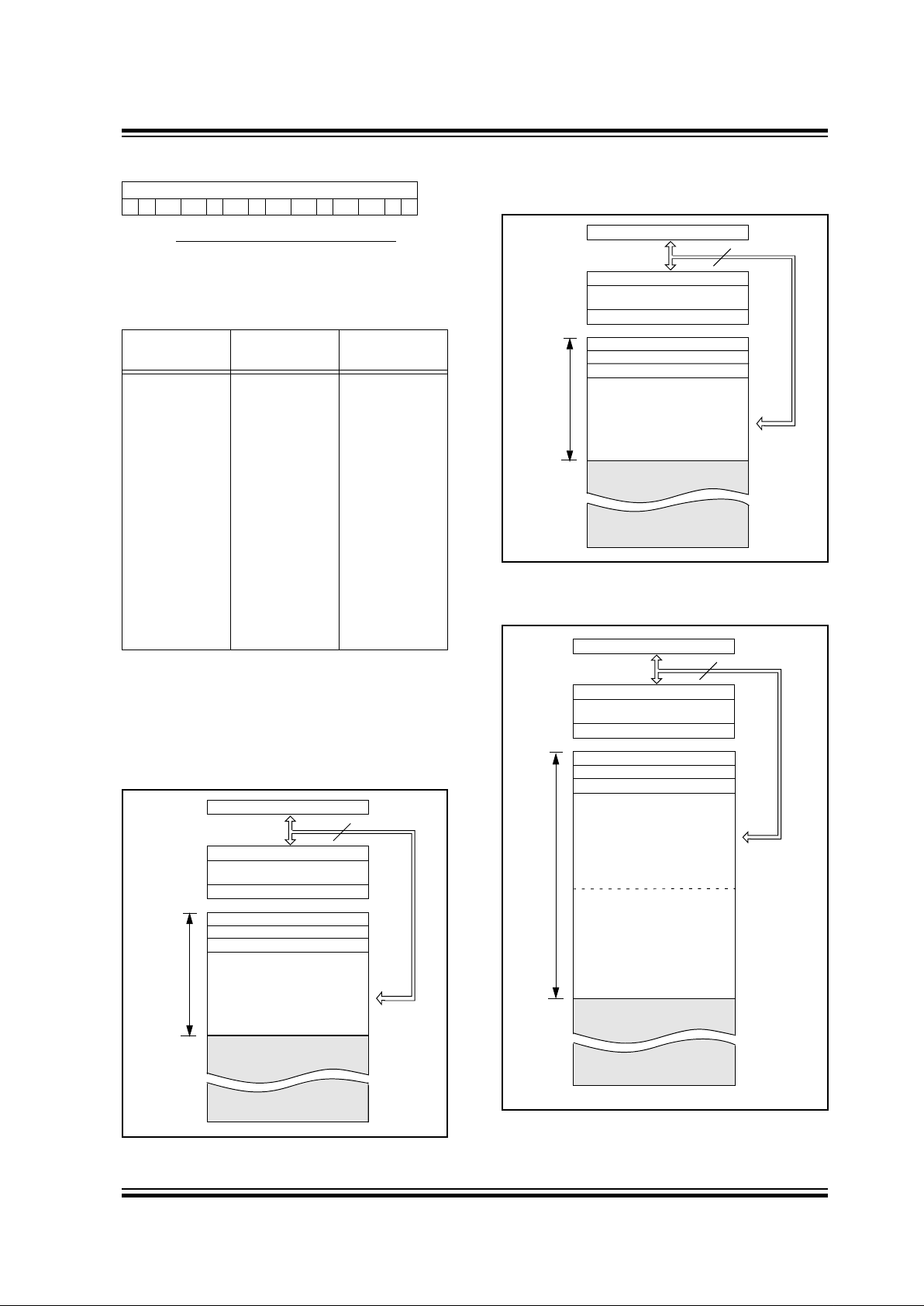
FIGURE 3-1: PIC16C61 BLOCK DIAGRAM
EPROM
Program
Memory
1K x 14
13
Data Bus
8
14
Program
Bus
Instruction reg
Program Counter
8 Level Stack
(13-bit)
RAM
File
Registers
36 x 8
Direct Addr
7
9
Addr MUX
Indirect
Addr
8
FSR reg
STATUS reg
MUX
ALU
W reg
Power-up
Timer
Oscillator
Start-up Timer
Power-on
Reset
Watchdog
Timer
Instruction
Decode &
Control
Timing
Generation
OSC1/CLKIN
OSC2/CLKOUT
MCLR
VDD, VSS
Timer0
3
PORTA
PORTB
RA1
RA4/T0CKI
RB0/INT
RB7:RB1
8
8
RAM Addr
(1)
Note 1: Higher order bits are from the STATUS register.
RA0
RA2
RA3

1997 Microchip Technology Inc. DS30234D-page 11
PIC16C6X
FIGURE 3-2: PIC16C62/62A/R62/64/64A/R64 BLOCK DIAGRAM
EPROM/
Program
Memory
2K x 14
13
Data Bus
8
14
Program
Bus
Instruction reg
Program Counter
8 Level Stack
(13-bit)
RAM
File
Registers
128 x 8
Direct Addr
7
RAM Addr
(1)
9
Addr MUX
Indirect
Addr
8
FSR reg
STATUS reg
MUX
ALU
W reg
Power-up
Timer
Oscillator
Start-up Timer
Power-on
Reset
Watchdog
Timer
Instruction
Decode &
Control
Timing
Generation
OSC1/CLKIN
OSC2/CLKOUT
MCLR
VDD, VSS
Synchronous
Serial Port
3
PORTA
PORTB
PORTC
PORTD
PORTE
RA4/T0CKI
RA5/SS
RB0/INT
RB7:RB1
RC0/T1OSO/T1CKI
(4)
RC1/T1OSI
(4)
RC2/CCP1
RC3/SCK/SCL
RC4/SDI/SDA
RC5/SDO
RC6
RC7
RE0/RD
RE1/WR
RE2/CS
RD0/PSP0
8
8
(Note 2)
Brown-out
Reset
(3)
ROM
Timer0
Timer1 Timer2 CCP1
RA1
RA0
RA2
RA3
RD1/PSP1
RD2/PSP2
RD3/PSP3
RD4/PSP4
RD5/PSP5
RD6/PSP6
RD7/PSP7
Parallel Slave
Port
Note 1: Higher order bits are from the STATUS register.
2: PORTD, PORTE and the Parallel Slave Port are not available on the PIC16C62/62A/R62.
3: Brown-out Reset is not available on the PIC16C62/64.
4: Pin functions T1OSI and T1OSO are swapped on the PIC16C62/64.

PIC16C6X
DS30234D-page 12 1997 Microchip Technology Inc.
FIGURE 3-3: PIC16C63/R63/65/65A/R65 BLOCK DIAGRAM
Synchronous
Serial Port
EPROM
Program
Memory
4K x 14
13
Data Bus
8
14
Program
Bus
Instruction reg
Program Counter
8 Level Stack
(13-bit)
RAM
File
Registers
192 x 8
Direct Addr
7
RAM Addr
(1)
9
Addr MUX
Indirect
Addr
8
FSR reg
STATUS reg
MUX
ALU
W reg
Power-up
Timer
Oscillator
Start-up Timer
Power-on
Reset
Watchdog
Timer
Instruction
Decode &
Control
Timing
Generation
OSC1/CLKIN
OSC2/CLKOUT
MCLR
VDD, VSS
3
PORTA
PORTB
PORTC
PORTD
PORTE
RA4/T0CKI
RA5/SS
RB0/INT
RB7:RB1
RC0/T1OSO/T1CKI
RC1/T1OSI/CCP2
RC2/CCP1
RC3/SCK/SCL
RC4/SDI/SDA
RC5/SDO
RC6/TX/CK
RC7/RX/DT
RE0/RD
RE1/WR
RE2/CS
8
8
Brown-out
Reset
(3)
(Note 2)
USART
Timer0 Timer1 Timer2
CCP2CCP1
RD0/PSP0
RD1/PSP1
RD2/PSP2
RD3/PSP3
RD4/PSP4
RD5/PSP5
RD6/PSP6
RD7/PSP7
RA1
RA0
RA2
RA3
Parallel Slave
Port
Note 1: Higher order bits are from the STATUS register.
2: PORTD, PORTE and the Parallel Slave Port are not available on the PIC16C63/R63.
3: Brown-out Reset is not available on the PIC16C65.
1997 Microchip Technology Inc. DS30234D-page 13
PIC16C6X
FIGURE 3-4: PIC16C66/67 BLOCK DIAGRAM
Synchronous
Serial Port
EPROM
Program
Memory
8K x 14
13
Data Bus
8
14
Program
Bus
Instruction reg
Program Counter
8 Level Stack
(13-bit)
RAM
File
Registers
368 x 8
Direct Addr
7
RAM Addr
(1)
9
Addr MUX
Indirect
Addr
8
FSR reg
STATUS reg
MUX
ALU
W reg
Power-up
Timer
Oscillator
Start-up Timer
Power-on
Reset
Watchdog
Timer
Instruction
Decode &
Control
Timing
Generation
OSC1/CLKIN
OSC2/CLKOUT
MCLR
VDD, VSS
3
PORTA
PORTB
PORTC
PORTD
PORTE
RA4/T0CKI
RA5/SS
RB0/INT
RB7:RB1
RC0/T1OSO/T1CKI
RC1/T1OSI/CCP2
RC2/CCP1
RC3/SCK/SCL
RC4/SDI/SDA
RC5/SDO
RC6/TX/CK
RC7/RX/DT
RE0/RD
RE1/WR
RE2/CS
8
8
Brown-out
Reset
(Note 2)
USART
Timer0 Timer1 Timer2
CCP2CCP1
RD0/PSP0
RD1/PSP1
RD2/PSP2
RD3/PSP3
RD4/PSP4
RD5/PSP5
RD6/PSP6
RD7/PSP7
RA1
RA0
RA2
RA3
Parallel Slave
Port
Note 1: Higher order bits are from the STATUS register.
2: PORTD, PORTE and the Parallel Slave Port are not available on the PIC16C66.
PIC16C6X
DS30234D-page 14 1997 Microchip Technology Inc.
TABLE 3-1: PIC16C61 PINOUT DESCRIPTION
Pin Name
DIP
Pin#
SOIC
Pin#
Pin Type
Buffer
Type
Description
OSC1/CLKIN 16 16 I
ST/CMOS
(1)
Oscillator crystal input/external clock source input.
OSC2/CLKOUT 15 15 O — Oscillator crystal output. Connects to crystal or resonator in crystal
oscillator mode. In RC mode, the pin outputs CLKOUT which has
1/4 the frequency of OSC1, and denotes the instruction cycle rate.
MCLR
/VPP
4 4 I/P ST Master clear reset input or programming voltage input. This pin is an
active low reset to the device.
PORTA is a bi-directional I/O port.
RA0 17 17 I/O TTL
RA1 18 18 I/O TTL
RA2 1 1 I/O TTL
RA3 2 2 I/O TTL
RA4/T0CKI 3 3 I/O ST RA4 can also be the clock input to the Timer0 timer/counter.
Output is open drain type.
PORTB is a bi-directional I/O port. PORTB can be software pro-
grammed for internal weak pull-up on all inputs.
RB0/INT 6 6 I/O TTL/ST
(2)
RB0 can also be the external interrupt pin.
RB1 7 7 I/O TTL
RB2 8 8 I/O TTL
RB3 9 9 I/O TTL
RB4 10 10 I/O TTL Interrupt on change pin.
RB5 11 11 I/O TTL Interrupt on change pin.
RB6 12 12 I/O TTL/ST
(3)
Interrupt on change pin. Serial programming clock.
RB7 13 13 I/O TTL/ST
(3)
Interrupt on change pin. Serial programming data.
VSS 5 5 P — Ground reference for logic and I/O pins.
VDD 14 14 P — Positive supply for logic and I/O pins.
Legend: I = input O = output I/O = input/output P = power
— = Not used TTL = TTL input ST = Schmitt Trigger input
Note 1: This buffer is a Schmitt Trigger input when configured in RC oscillator mode and a CMOS input otherwise.
2: This buffer is a Schmitt Trigger input when configured as the external interrupt.
3: This buffer is a Schmitt Trigger input when used in serial programming mode.

1997 Microchip Technology Inc. DS30234D-page 15
PIC16C6X
TABLE 3-2: PIC16C62/62A/R62/63/R63/66 PINOUT DESCRIPTION
Pin Name Pin# Pin Type
Buffer
Type
Description
OSC1/CLKIN 9 I
ST/CMOS
(3)
Oscillator crystal input/external clock source input.
OSC2/CLKOUT 10 O — Oscillator crystal output. Connects to crystal or resonator in crys-
tal oscillator mode. In RC mode, the pin outputs CLKOUT which
has 1/4 the frequency of OSC1, and denotes the instruction cycle
rate.
M
CLR/VPP
1 I/P ST Master clear reset input or programming voltage input. This pin is
an active low reset to the device.
PORTA is a bi-directional I/O port.
RA0 2 I/O TTL
RA1 3 I/O TTL
RA2 4 I/O TTL
RA3 5 I/O TTL
RA4/T0CKI 6 I/O ST RA4 can also be the clock input to the Timer0 timer/counter.
Output is open drain type.
RA5/SS 7 I/O TTL RA5 can also be the slave select for the synchronous serial
port.
PORTB is a bi-directional I/O port. PORTB can be software pro-
grammed for internal weak pull-up on all inputs.
RB0/INT 21 I/O TTL/ST
(4)
RB0 can also be the external interrupt pin.
RB1 22 I/O TTL
RB2 23 I/O TTL
RB3 24 I/O TTL
RB4 25 I/O TTL Interrupt on change pin.
RB5 26 I/O TTL Interrupt on change pin.
RB6 27 I/O TTL/ST
(5)
Interrupt on change pin. Serial programming clock.
RB7 28 I/O TTL/ST
(5)
Interrupt on change pin. Serial programming data.
PORTC is a bi-directional I/O port.
RC0/T1OSO
(1)
/T1CKI
11 I/O ST RC0 can also be the Timer1 oscillator output
(1)
or Timer1
clock input.
RC1/T1OSI
(1)
/CCP2
(2)
12 I/O ST RC1 can also be the Timer1 oscillator input
(1)
or Capture2
input/Compare2 output/PWM2 output
(2)
.
RC2/CCP1 13 I/O ST RC2 can also be the Capture1 input/Compare1 out-
put/PWM1 output.
RC3/SCK/SCL 14 I/O ST RC3 can also be the synchronous serial clock input/output
for both SPI and I
2
C modes.
RC4/SDI/SDA 15 I/O ST RC4 can also be the SPI Data In (SPI mode) or
data I/O (I
2
C mode).
RC5/SDO 16 I/O ST RC5 can also be the SPI Data Out (SPI mode).
RC6/TX/CK
(2)
17 I/O ST RC6 can also be the USART Asynchronous Transmit
(2)
or
Synchronous Clock
(2)
.
RC7/RX/DT
(2)
18 I/O ST RC7 can also be the USART Asynchronous Receive
(2)
or
Synchronous Data
(2)
.
VSS 8,19 P — Ground reference for logic and I/O pins.
VDD 20 P — Positive supply for logic and I/O pins.
Legend: I = input O = output I/O = input/output P = power
— = Not used TTL = TTL input ST = Schmitt Trigger input
Note 1: Pin functions T1OSO and T1OSI are reversed on the PIC16C62.
2: The USART and CCP2 are not available on the PIC16C62/62A/R62.
3: This buffer is a Schmitt Trigger input when configured in RC oscillator mode and a CMOS input otherwise.
4: This buffer is a Schmitt Trigger input when configured as the external interrupt.
5: This buffer is a Schmitt Trigger input when used in serial programming mode.
PIC16C6X
DS30234D-page 16 1997 Microchip Technology Inc.
TABLE 3-3: PIC16C64/64A/R64/65/65A/R65/67 PINOUT DESCRIPTION
Pin Name
DIP
Pin#
PLCC
Pin#
TQFP
MQFP
Pin#
Pin
Type
Buffer
Type
Description
OSC1/CLKIN 13 14 30 I
ST/CMOS
(3)
Oscillator crystal input/external clock source input.
OSC2/CLKOUT 14 15 31 O — Oscillator crystal output. Connects to crystal or resonator in
crystal oscillator mode. In RC mode, the pin outputs CLK-
OUT which has 1/4 the frequency of OSC1, and denotes the
instruction cycle rate.
MCLR
/VPP
1 2 18 I/P ST Master clear reset input or programming voltage input. This
pin is an active low reset to the device.
PORTA is a bi-directional I/O port.
RA0 2 3 19 I/O TTL
RA1 3 4 20 I/O TTL
RA2 4 5 21 I/O TTL
RA3 5 6 22 I/O TTL
RA4/T0CKI 6 7 23 I/O ST RA4 can also be the clock input to the Timer0
timer/counter. Output is open drain type.
RA5/SS 7 8 24 I/O TTL RA5 can also be the slave select for the synchronous
serial port.
PORTB is a bi-directional I/O port. PORTB can be software
programmed for internal weak pull-up on all inputs.
RB0/INT 33 36 8 I/O TTL/ST
(4)
RB0 can also be the external interrupt pin.
RB1 34 37 9 I/O TTL
RB2 35 38 10 I/O TTL
RB3 36 39 11 I/O TTL
RB4 37 41 14 I/O TTL Interrupt on change pin.
RB5 38 42 15 I/O TTL Interrupt on change pin.
RB6 39 43 16 I/O TTL/ST
(5)
Interrupt on change pin. Serial programming clock.
RB7 40 44 17 I/O TTL/ST
(5)
Interrupt on change pin. Serial programming data.
PORTC is a bi-directional I/O port.
RC0/T1OSO
(1)
/T1CKI 15 16 32 I/O ST RC0 can also be the Timer1 oscillator output
(1)
or
Timer1 clock input.
RC1/T1OSI
(1)
/CCP2
(2)
16 18 35 I/O ST RC1 can also be the Timer1 oscillator input
(1)
or
Capture2 input/Compare2 output/PWM2 output
(2)
.
RC2/CCP1 17 19 36 I/O ST RC2 can also be the Capture1 input/Compare1 out-
put/PWM1 output.
RC3/SCK/SCL 18 20 37 I/O ST RC3 can also be the synchronous serial clock input/out-
put for both SPI and I
2
C modes.
RC4/SDI/SDA 23 25 42 I/O ST RC4 can also be the SPI Data In (SPI mode) or
data I/O (I
2
C mode).
RC5/SDO 24 26 43 I/O ST RC5 can also be the SPI Data Out (SPI mode).
RC6/TX/CK
(2)
25 27 44 I/O ST RC6 can also be the USART Asynchronous Transmit
(2)
or Synchronous Clock
(2)
.
RC7/RX/DT
(2)
26 29 1 I/O ST RC7 can also be the USART Asynchronous Receive
(2)
or Synchronous Data
(2)
.
Legend: I = input O = output I/O = input/output P = power
— = Not used TTL = TTL input ST = Schmitt Trigger input
Note 1: Pin functions T1OSO and T1OSI are reversed on the PIC16C64.
2: CCP2 and the USART are not available on the PIC16C64/64A/R64.
3: This buffer is a Schmitt Trigger input when configured in RC oscillator mode and a CMOS input otherwise.
4: This buffer is a Schmitt Trigger input when configured as the external interrupt.
5: This buffer is a Schmitt Trigger input when used in serial programming mode.
6: This buffer is a Schmitt Trigger input when configured as general purpose I/O and a TTL input when used in the Parallel Slave
Port mode (for interfacing to a microprocessor bus).
1997 Microchip Technology Inc. DS30234D-page 17
PIC16C6X
PORTD can be a bi-directional I/O port or parallel slave port
for interfacing to a microprocessor bus.
RD0/PSP0 19 21 38 I/O ST/TTL
(6)
RD1/PSP1 20 22 39 I/O ST/TTL
(6)
RD2/PSP2 21 23 40 I/O ST/TTL
(6)
RD3/PSP3 22 24 41 I/O ST/TTL
(6)
RD4/PSP4 27 30 2 I/O ST/TTL
(6)
RD5/PSP5 28 31 3 I/O ST/TTL
(6)
RD6/PSP6 29 32 4 I/O ST/TTL
(6)
RD7/PSP7 30 33 5 I/O ST/TTL
(6)
PORTE is a bi-directional I/O port.
RE0/RD 8 9 25 I/O ST/TTL
(6)
RE0 can also be read control for the parallel slave port.
RE1/WR 9 10 26 I/O ST/TTL
(6)
RE1 can also be write control for the parallel slave port.
RE2/CS 10 11 27 I/O ST/TTL
(6)
RE2 can also be select control for the parallel slave port.
VSS 12,31 13,34 6,29 P — Ground reference for logic and I/O pins.
VDD 11,32 12,35 7,28 P — Positive supply for logic and I/O pins.
NC — 1,17,
28,40
12,13,
33,34
— — These pins are not internally connected. These pins should
be left unconnected.
TABLE 3-3: PIC16C64/64A/R64/65/65A/R65/67 PINOUT DESCRIPTION (Cont.’d)
Pin Name
DIP
Pin#
PLCC
Pin#
TQFP
MQFP
Pin#
Pin
Type
Buffer
Type
Description
Legend: I = input O = output I/O = input/output P = power
— = Not used TTL = TTL input ST = Schmitt Trigger input
Note 1: Pin functions T1OSO and T1OSI are reversed on the PIC16C64.
2: CCP2 and the USART are not available on the PIC16C64/64A/R64.
3: This buffer is a Schmitt Trigger input when configured in RC oscillator mode and a CMOS input otherwise.
4: This buffer is a Schmitt Trigger input when configured as the external interrupt.
5: This buffer is a Schmitt Trigger input when used in serial programming mode.
6: This buffer is a Schmitt Trigger input when configured as general purpose I/O and a TTL input when used in the Parallel Slave
Port mode (for interfacing to a microprocessor bus).
PIC16C6X
DS30234D-page 18 1997 Microchip Technology Inc.
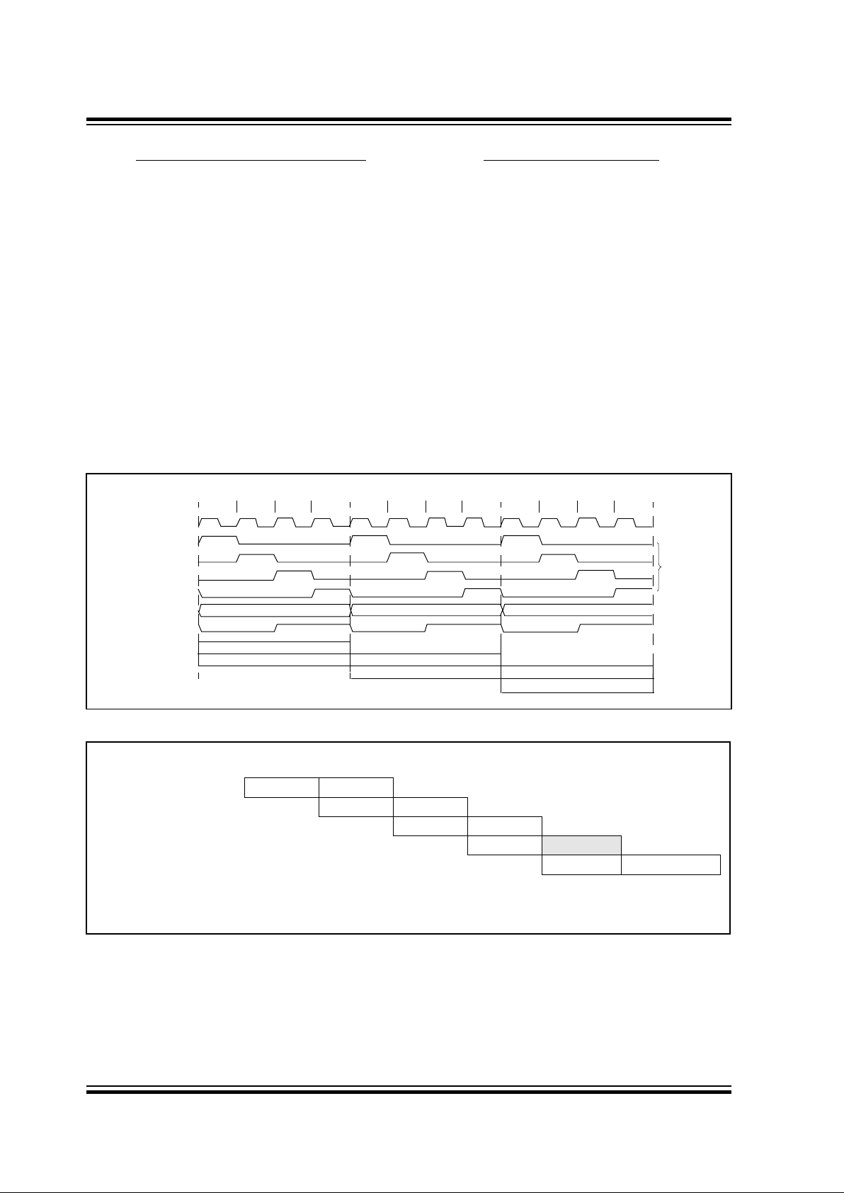
3.1 Clocking Scheme/Instruction Cycle
The clock input (from OSC1) is internally divided by
four to generate four non-overlapping quadrature
clocks namely Q1, Q2, Q3, and Q4. Internally, the pro-
gram counter (PC) is incremented every Q1, the
instruction is fetched from the program memory and
latched into the instruction register in Q4. The instruc-
tion is decoded and executed during the following Q1
through Q4. The clock and instruction execution flow is
shown in Figure 3-5.
3.2 Instruction Flow/Pipelining
An “Instruction Cycle” consists of four Q cycles (Q1,
Q2, Q3, and Q4). The instruction f etch and execute are
pipelined such that fetch takes one instruction cycle
while decode and execute takes another instruction
cycle. However, due to the pipelining, each instruction
effectively executes in one cycle. If an instruction
causes the program counter to change (e.g. GOTO)
then two cycles are required to complete the instruction
(Example 3-1).
A fetch cycle begins with the program counter (PC)
incrementing in Q1.
In the execution cycle, the f etched instruction is latched
into the “Instruction Register (IR)” in cycle Q1. This
instruction is then decoded and executed during the
Q2, Q3, and Q4 cycles. Data memory is read during Q2
(operand read) and written during Q4 (destination
write).
FIGURE 3-5: CLOCK/INSTRUCTION CYCLE
EXAMPLE 3-1: INSTRUCTION PIPELINE FLOW
Q1
Q2 Q3 Q4
Q1
Q2 Q3 Q4
Q1
Q2 Q3 Q4
OSC1
Q1
Q2
Q3
Q4
PC
(Program counter)
OSC2/CLKOUT
(RC mode)
PC PC+1 PC+2
Fetch INST (PC)
Execute INST (PC-1)
Fetch INST (PC+1)
Execute INST (PC) Fetch INST (PC+2)
Execute INST (PC+1)
Internal
Phase
Clock
All instructions are single cycle, except for any program branches. These take two cycles since the fetch
instruction is “flushed” from the pipeline while the new instruction is being fetched and then executed.
Tcy0 Tcy1 Tcy2 Tcy3 Tcy4 Tcy5
1. MOVLW 55h
Fetch 1 Execute 1
2. MOVWF PORTB
Fetch 2 Execute 2
3. CALL SUB_1
Fetch 3 Execute 3
4. BSF PORTA, BIT3 (Forced NOP)
Fetch 4 Flush
5. Instruction @ address SUB_1
Fetch SUB_1 Execute SUB_1
1997 Microchip Technology Inc. DS30234D-page 19
PIC16C6X
4.0 MEMORY ORGANIZATION
4.1 Program Memory Organization
The PIC16C6X family has a 13-bit program counter
capable of addressing an 8K x 14 program memory
space. The amount of program memory available to
each device is listed below:
For those devices with less than 8K program memory,
accessing a location above the physically implemented
address will cause a wraparound.
The reset vector is at 0000h and the interrupt vector is
at 0004h.
FIGURE 4-1: PIC16C61 PROGRAM
MEMORY MAP AND STACK
Applicable Devices
61 62 62A R62 63 R63 64 64A R64 65 65A R65 66 67
Device
Program
Memory
Address Range
PIC16C61 1K x 14 0000h-03FFh
PIC16C62 2K x 14 0000h-07FFh
PIC16C62A 2K x 14 0000h-07FFh
PIC16CR62 2K x 14 0000h-07FFh
PIC16C63 4K x 14 0000h-0FFFh
PIC16CR63 4K x 14 0000h-0FFFh
PIC16C64 2K x 14 0000h-07FFh
PIC16C64A 2K x 14 0000h-07FFh
PIC16CR64 2K x 14 0000h-07FFh
PIC16C65 4K x 14 0000h-0FFFh
PIC16C65A 4K x 14 0000h-0FFFh
PIC16CR65 4K x 14 0000h-0FFFh
PIC16C66 8K x 14 0000h-1FFFh
PIC16C67 8K x 14 0000h-1FFFh
PC<12:0>
Stack Level 1
•
Stack Level 8
•
•
User Memory
Space
CALL, RETURN
RETFIE, RETLW
13
0000h
0004h
1FFFh
03FFh
0400h
On-chip Program
Memory
0005h
Reset Vector
Peripheral Interrupt Vector
FIGURE 4-2: PIC16C62/62A/R62/64/64A/
R64 PROGRAM MEMORY
MAP AND STACK
FIGURE 4-3: PIC16C63/R63/65/65A/R65
PROGRAM MEMORY MAP
AND STACK
PC<12:0>
Stack Level 1
Stack Level 8
User Memory
Space
CALL, RETURN
RETFIE, RETLW
13
0000h
0004h
1FFFh
07FFh
0800h
On-chip Program
Memory
0005h
Reset Vector
Peripheral Interrupt Vector
•
•
•
PC<12:0>
Stack Level 1
Stack Level 8
User Memory
Space
CALL, RETURN
RETFIE, RETLW
13
0000h
0004h
1FFFh
07FFh
0FFFh
0800h
1000h
On-chip Program
Memory (Page 0)
On-chip Program
Memory (Page 1)
0005h
Reset Vector
Peripheral Interrupt Vector
•
•
•
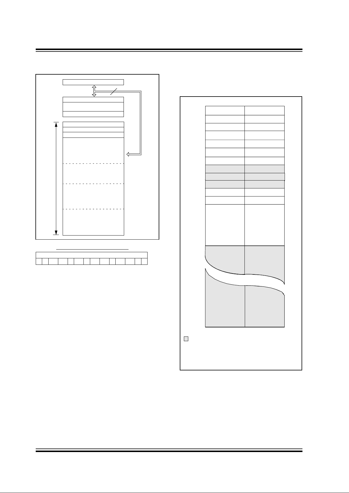
PIC16C6X
DS30234D-page 20 1997 Microchip Technology Inc.
FIGURE 4-4: PIC16C66/67 PROGRAM
MEMORY MAP AND STACK
4.2 Data Memory Organization
The data memory is partitioned into multiple banks
which contain the General Purpose Registers and the
Special Function Registers. Bits RP1 and RP0 are the
bank select bits.
RP1:RP0 (STATUS<6:5>)
= 00 → Bank0
= 01 → Bank1
= 10 → Bank2
= 11 → Bank3
Each bank extends up to 7Fh (128 bytes). The lower
locations of each bank are reserved for the Special
Function Registers. Above the Special Function Regis-
ters are General Purpose Registers, implemented as
static RAM. All implemented banks contain special
function registers. Some “high use” special function
registers from one bank may be mirrored in another
bank for code reduction and quicker access.
4.2.1 GENERAL PURPOSE REGISTERS
These registers are accessed either directly or indi-
rectly through the File Select Register (FSR)
(Section 4.5).
Applicable Devices
61 62 62A R62 63 R63 64 64A R64 65 65A R65 66 67
PC<12:0>
Stack Level 1
Stack Level 8
User Memory
Space
CALL, RETURN
RETFIE, RETLW
13
0000h
0004h
0FFFh
1000h
On-chip Program
Memory (Page 0)
On-chip Program
Memory (Page 1)
0005h
Reset Vector
Peripheral Interrupt Vector
•
•
•
07FFh
0800h
On-chip Program
Memory (Page 2)
On-chip Program
Memory (Page 3)
17FFh
1800h
1FFFh
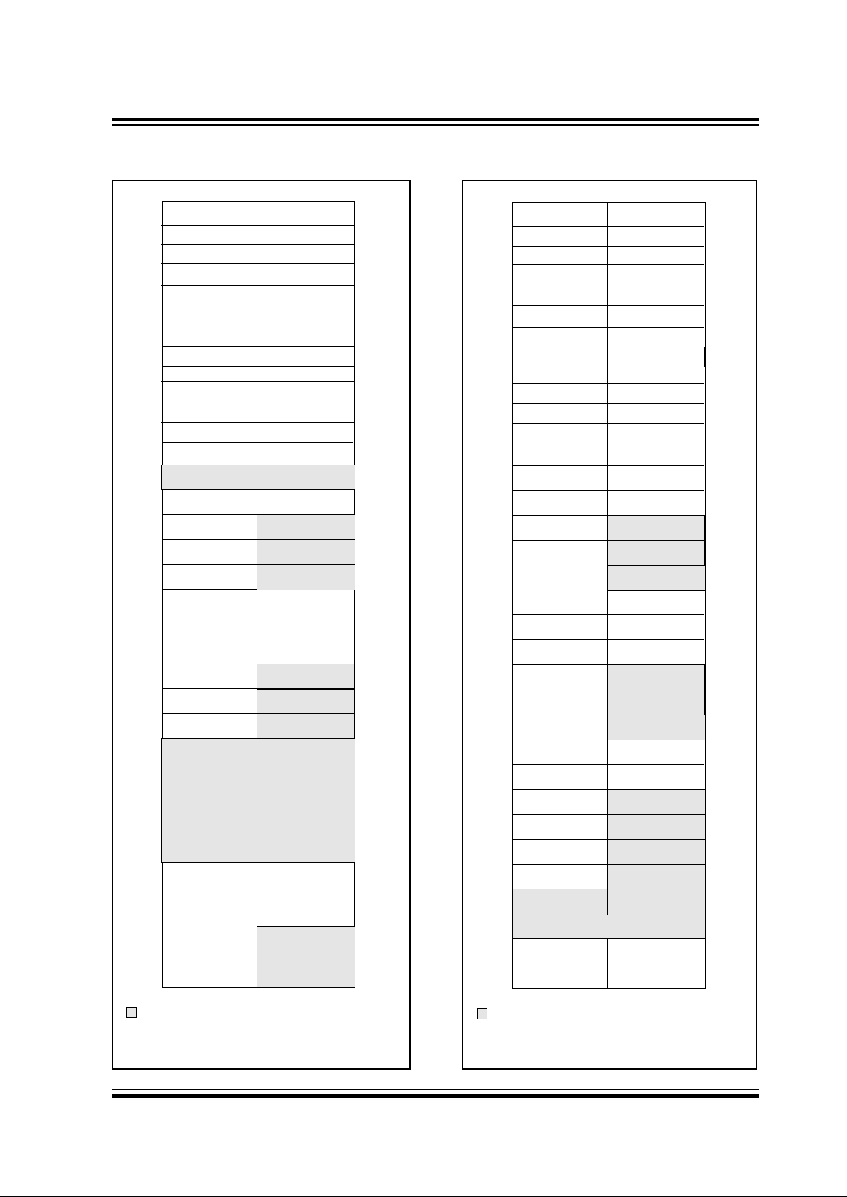
For the PIC16C61, general purpose register locations
8Ch-AFh of Bank 1 are not physically implemented.
These locations are mapped into 0Ch-2Fh of Bank 0.
FIGURE 4-5: PIC16C61 REGISTER FILE
MAP
File Address
00h
01h
02h
03h
04h
05h
06h
07h
08h
09h
0Ah
0Bh
0Ch
2Fh
30h
7Fh
80h
81h
82h
83h
84h
85h
86h
87h
88h
89h
8Ah
8Bh
8Ch
AFh
B0h
FFh
Bank 0
Bank 1
INDF
(1)
INDF
(1)
TMR0 OPTION
PCL
STATUS
FSR
PORTA
PORTB
PCLATH
INTCON
General
Purpose
Register
PCL
STATUS
FSR
TRISA
TRISB
PCLATH
INTCON
Mapped
in Bank 0
(2)
Unimplemented data memory location; read as '0'.
Note 1: Not a physical register.
2: These locations are unimplemented in
Bank 1. Any access to these locations will
access the corresponding Bank 0 register.
File Address
1997 Microchip Technology Inc. DS30234D-page 21
PIC16C6X
FIGURE 4-6: PIC16C62/62A/R62/64/64A/
R64 REGISTER FILE MAP
File Address
00h
01h
02h
03h
04h
05h
06h
07h
08h
09h
0Ah
0Bh
0Ch
7Fh
80h
81h
82h
83h
84h
85h
86h
87h
88h
89h
8Ah
8Bh
8Ch
FFh
Bank 0
Bank 1
INDF
(1)
INDF
(1)
TMR0 OPTION
PCL
STATUS
FSR
PORTA
PORTB
PORTD
(2)
PORTE
(2)
PCLATH
INTCON
PCL
STATUS
FSR
TRISA
TRISB
TRISD
(2)
TRISE
(2)
PCLATH
INTCON
Unimplemented data memory location; read as '0'.
PORTC TRISC
PIR1 PIE1
TMR1L PCON
TMR1H
T1CON
TMR2
T2CON
PR2
SSPBUF
SSPADD
SSPSTAT
SSPCON
CCPR1L
CCPR1H
CCP1CON
General
Purpose
Register
0Dh
8Dh
0Eh
8Eh
0Fh
8Fh
10h
90h
11h
91h
12h
92h
13h
93h
14h
94h
15h
95h
16h
96h
17h
97h
18h
98h
1Fh
9Fh
20h
A0h
BFh
C0h
General
Purpose
Register
Note 1: Not a physical register.
2: PORTD and PORTE are not available on
the PIC16C62/62A/R62.
File Address
FIGURE 4-7: PIC16C63/R63/65/65A/R65
REGISTER FILE MAP
File Address
00h
01h
02h
03h
04h
05h
06h
07h
08h
09h
0Ah
0Bh
0Ch
7Fh
80h
81h
82h
83h
84h
85h
86h
87h
88h
89h
8Ah
8Bh
8Ch
FFh
Bank 0
Bank 1
INDF
(1)
INDF
(1)
TMR0 OPTION
PCL
STATUS
FSR
PORTA
PORTB
PORTD
(2)
PORTE
(2)
PCLATH
INTCON
PCL
STATUS
FSR
TRISA
TRISB
TRISD
(2)
TRISE
(2)
PCLATH
INTCON
Unimplemented data memory location; read as '0'.
PORTC TRISC
PIR1 PIE1
PIR2 PIE2
TMR1L PCON
TMR1H
T1CON
TMR2
T2CON
PR2
SSPBUF
SSPADD
SSPSTAT
SSPCON
CCPR1L
CCPR1H
CCP1CON
CCPR2L
CCPR2H
CCP2CON
RCSTA
TXREG
RCREG
TXSTA
SPBRG
General
Purpose
Register
General
Purpose
Register
0Dh
8Dh
0Eh
8Eh
0Fh
8Fh
10h
90h
11h
91h
12h
92h
13h
93h
14h
94h
15h
95h
16h
96h
17h
97h
18h
98h
19h
99h
1Ah
9Ah
1Bh
9Bh
1Ch
9Ch
1Dh
9Dh
1Eh
9Eh
1Fh
9Fh
20h
A0h
Note 1: Not a physical register
2: PORTD and PORTE are not available on
the PIC16C63/R63.
File Address

PIC16C6X
DS30234D-page 22 1997 Microchip Technology Inc.
FIGURE 4-8: PIC16C66/67 DATA MEMORY MAP
Indirect addr.
(*)
TMR0
PCL
STATUS
FSR
PORTA
PORTB
PORTC
PCLATH
INTCON
PIR1
TMR1L
TMR1H
T1CON
TMR2
T2CON
SSPBUF
SSPCON
CCPR1L
CCPR1H
CCP1CON
OPTION
PCL
STATUS
FSR
TRISA
TRISB
TRISC
PCLATH
INTCON
PIE1
PCON
PR2
SSPADD
SSPSTAT
00h
01h
02h
03h
04h
05h
06h
07h
08h
09h
0Ah
0Bh
0Ch
0Dh
0Eh
0Fh
10h
11h
12h
13h
14h
15h
16h
17h
18h
19h
1Ah
1Bh
1Ch
1Dh
1Eh
1Fh
80h
81h
82h
83h
84h
85h
86h
87h
88h
89h
8Ah
8Bh
8Ch
8Dh
8Eh
8Fh
90h
91h
92h
93h
94h
95h
96h
97h
98h
99h
9Ah
9Bh
9Ch
9Dh
9Eh
9Fh
20h
A0h
7Fh
FFh
Bank 0
Bank 1
Unimplemented data memory locations, read as '0'.
* Not a physical register.
These registers are not implemented on the PIC16C66.
Note: The upper 16 bytes of data memory in banks 1, 2, and 3 are mapped in Bank 0. This may require
relocation of data memory usage in the user application code if upgrading to the PIC16C66/67.
File
Address
Indirect addr.
(*)
Indirect addr.
(*)
PCL
STATUS
FSR
PCLATH
INTCON
PCL
STATUS
FSR
PCLATH
INTCON
100h
101h
102h
103h
104h
105h
106h
107h
108h
109h
10Ah
10Bh
10Ch
10Dh
10Eh
10Fh
110h
111h
112h
113h
114h
115h
116h
117h
118h
119h
11Ah
11Bh
11Ch
11Dh
11Eh
11Fh
180h
181h
182h
183h
184h
185h
186h
187h
188h
189h
18Ah
18Bh
18Ch
18Dh
18Eh
18Fh
190h
191h
192h
193h
194h
195h
196h
197h
198h
199h
19Ah
19Bh
19Ch
19Dh
19Eh
19Fh
120h
1A0h
17Fh
1FFh
Bank 2
Bank 3
Indirect addr.
(*)
PORTD
PORTE
TRISD
TRISE
TMR0
OPTION
PIR2
PIE2
RCSTA
TXREG
RCREG
CCPR2L
CCPR2H
CCP2CON
TXSTA
SPBRG
General
Purpose
Register
General
Purpose
Register
General
Purpose
Register
General
Purpose
Register
1EFh
1F0h
EFh
F0h
16Fh
170h
General
Purpose
Register
General
Purpose
Register
TRISB
PORTB
96 Bytes
80 Bytes 80 Bytes 80 Bytes
16 Bytes
16 Bytes
(1)
(1)
(1)
(1)
accesses
70h-7Fh
in Bank 0
accesses
70h-7Fh
in Bank 0
accesses
70h-7Fh
in Bank 0

1997 Microchip Technology Inc. DS30234D-page 23
PIC16C6X
4.2.2 SPECIAL FUNCTION REGISTERS:
The Special Function Registers are registers used by
the CPU and peripheral modules for controlling the
desired operation of the device. These registers are
implemented as static RAM.
The special function registers can be classified into two
sets (core and peripheral). The registers associated
with the “core” functions are described in this section
and those related to the operation of the peripheral fea-
tures are described in the section of that peripheral fea-
ture.
TABLE 4-1: SPECIAL FUNCTION REGISTERS FOR THE PIC16C61
Address Name Bit 7 Bit 6 Bit 5 Bit 4 Bit 3 Bit 2 Bit 1 Bit 0
Value on:
POR
Value on
all other
resets
(3)
Bank 0
00h
(1)
INDF Addressing this location uses contents of FSR to address data memory (not a physical register) 0000 0000 0000 0000
01h TMR0 Timer0 module’s register xxxx xxxx uuuu uuuu
02h
(1)
PCL Program Counter's (PC) Least Significant Byte 0000 0000 0000 0000
03h
(1)
STATUS
IRP
(4)
RP1
(4)
RP0 TO PD ZDCC0001 1xxx 000q quuu
04h
(1)
FSR Indirect data memory address pointer xxxx xxxx uuuu uuuu
05h PORTA
— — — PORTA Data Latch when written: PORTA pins when read ---x xxxx ---u uuuu
06h PORTB PORTB Data Latch when written: PORTB pins when read xxxx xxxx uuuu uuuu
07h — Unimplemented
— —
08h
—
Unimplemented
— —
09h
—
Unimplemented
— —
0Ah
(1,2)
PCLATH — — —
Write Buffer for the upper 5 bits of the Program Counter
---0 0000 ---0 0000
0Bh
(1)
INTCON GIE — T0IE INTE RBIE T0IF INTF RBIF 0-00 000x 0-00 000u
Bank 1
80h
(1)
INDF Addressing this location uses contents of FSR to address data memory (not a physical register) 0000 0000 0000 0000
81h OPTION RBPU
INTEDG T0CS T0SE PSA PS2 PS1 PS0 1111 1111 1111 1111
82h
(1)
PCL Program Counter's (PC) Least Significant Byte 0000 0000 0000 0000
83h
(1)
STATUS
IRP
(4)
RP1
(4)
RP0 TO PD ZDCC0001 1xxx 000q quuu
84h
(1)
FSR Indirect data memory address pointer xxxx xxxx uuuu uuuu
85h TRISA
— — — PORTA Data Direction Register ---1 1111 ---1 1111
86h TRISB PORTB Data Direction Control Register 1111 1111 1111 1111
87h – Unimplemented
— —
88h
– Unimplemented
— —
89h
–
Unimplemented
— —
8Ah
(1,2)
PCLATH — — —
Write Buffer for the upper 5 bits of the Program Counter
---0 0000 ---0 0000
8Bh
(1)
INTCON GIE — T0IE INTE RBIE T0IF INTF RBIF 0-00 000x 0-00 000u
Legend: x = unknown, u = unchanged, q = value depends on condition, - = unimplemented locations read as '0'.
Shaded locations are unimplemented and read as ‘0’
Note 1: These registers can be addressed from either bank.
2: The upper byte of the Program Counter (PC) is not directly accessible. PCLATH is a holding register for the PC whose con-
tents are transferred to the upper byte of the program counter. (PC<12:8>)
3: Other (non power-up) resets include external reset through MCLR and the Watchdog Timer Reset.
4: The IRP and RP1 bits are reserved on the PIC16C61, always maintain these bits clear.
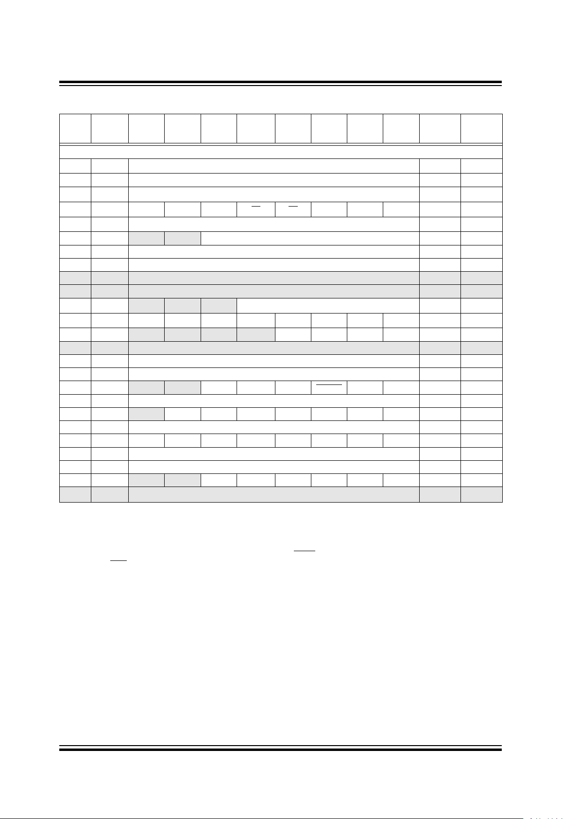
PIC16C6X
DS30234D-page 24 1997 Microchip Technology Inc.
TABLE 4-2: SPECIAL FUNCTION REGISTERS FOR THE PIC16C62/62A/R62
Address Name Bit 7 Bit 6 Bit 5 Bit 4 Bit 3 Bit 2 Bit 1 Bit 0
Value on:
POR,
BOR
Value on
all other
resets
(3)
Bank 0
00h
(1)
INDF Addressing this location uses contents of FSR to address data memory (not a physical register) 0000 0000 0000 0000
01h TMR0 Timer0 module’s register xxxx xxxx uuuu uuuu
02h
(1)
PCL Program Counter's (PC) Least Significant Byte 0000 0000 0000 0000
03h
(1)
STATUS
IRP
(5)
RP1
(5)
RP0 TO PD ZDCC0001 1xxx 000q quuu
04h
(1)
FSR Indirect data memory address pointer xxxx xxxx uuuu uuuu
05h PORTA
— — PORTA Data Latch when written: PORTA pins when read --xx xxxx --uu uuuu
06h PORTB PORTB Data Latch when written: PORTB pins when read xxxx xxxx uuuu uuuu
07h PORTC PORTC Data Latch when written: PORTC pins when read xxxx xxxx uuuu uuuu
08h — Unimplemented — —
09h — Unimplemented — —
0Ah
(1,2)
PCLATH — — —
Write Buffer for the upper 5 bits of the Program Counter
---0 0000 ---0 0000
0Bh
(1)
INTCON GIE PEIE T0IE INTE RBIE T0IF INTF RBIF 0000 000x 0000 000u
0Ch PIR1
(6) (6) — — SSPIF CCP1IF TMR2IF TMR1IF 00-- 0000 00-- 0000
0Dh — Unimplemented — —
0Eh TMR1L Holding register for the Least Significant Byte of the 16-bit TMR1 register xxxx xxxx uuuu uuuu
0Fh TMR1H Holding register for the Most Significant Byte of the 16-bit TMR1 register xxxx xxxx uuuu uuuu
10h T1CON — — T1CKPS1 T1CKPS0 T1OSCEN T1SYNC TMR1CS TMR1ON --00 0000 --uu uuuu
11h TMR2 Timer2 module’s register 0000 0000 0000 0000
12h T2CON — TOUTPS3 TOUTPS2 TOUTPS1 TOUTPS0 TMR2ON T2CKPS1 T2CKPS0 -000 0000 -000 0000
13h SSPBUF Synchronous Serial Port Receive Buffer/Transmit Register xxxx xxxx uuuu uuuu
14h SSPCON WCOL SSPOV SSPEN CKP SSPM3 SSPM2 SSPM1 SSPM0 0000 0000 0000 0000
15h CCPR1L Capture/Compare/PWM1 (LSB) xxxx xxxx uuuu uuuu
16h CCPR1H Capture/Compare/PWM1 (MSB) xxxx xxxx uuuu uuuu
17h CCP1CON — — CCP1X CCP1Y CCP1M3 CCP1M2 CCP1M1 CCP1M0 --00 0000 --00 0000
18h-1Fh
— Unimplemented
— —
Legend: x = unknown, u = unchanged, q = value depends on condition, - = unimplemented location read as '0'.
Shaded locations are unimplemented, read as ‘0’.
Note 1: These registers can be addressed from either bank.
2: The upper byte of the Program Counter (PC) is not directly accessible. PCLATH is a holding register for the PC whose
contents are transferred to the upper byte of the program counter. (PC<12:8>)
3: Other (non power-up) resets include external reset through MCLR and the Watchdog Timer reset.
4: The BOR bit is reserved on the PIC16C62, always maintain this bit set.
5: The IRP and RP1 bits are reserved on the PIC16C62/62A/R62, always maintain these bits clear.
6: PIE1<7:6> and PIR1<7:6> are reserved on the PIC16C62/62A/R62, always maintain these bits clear.
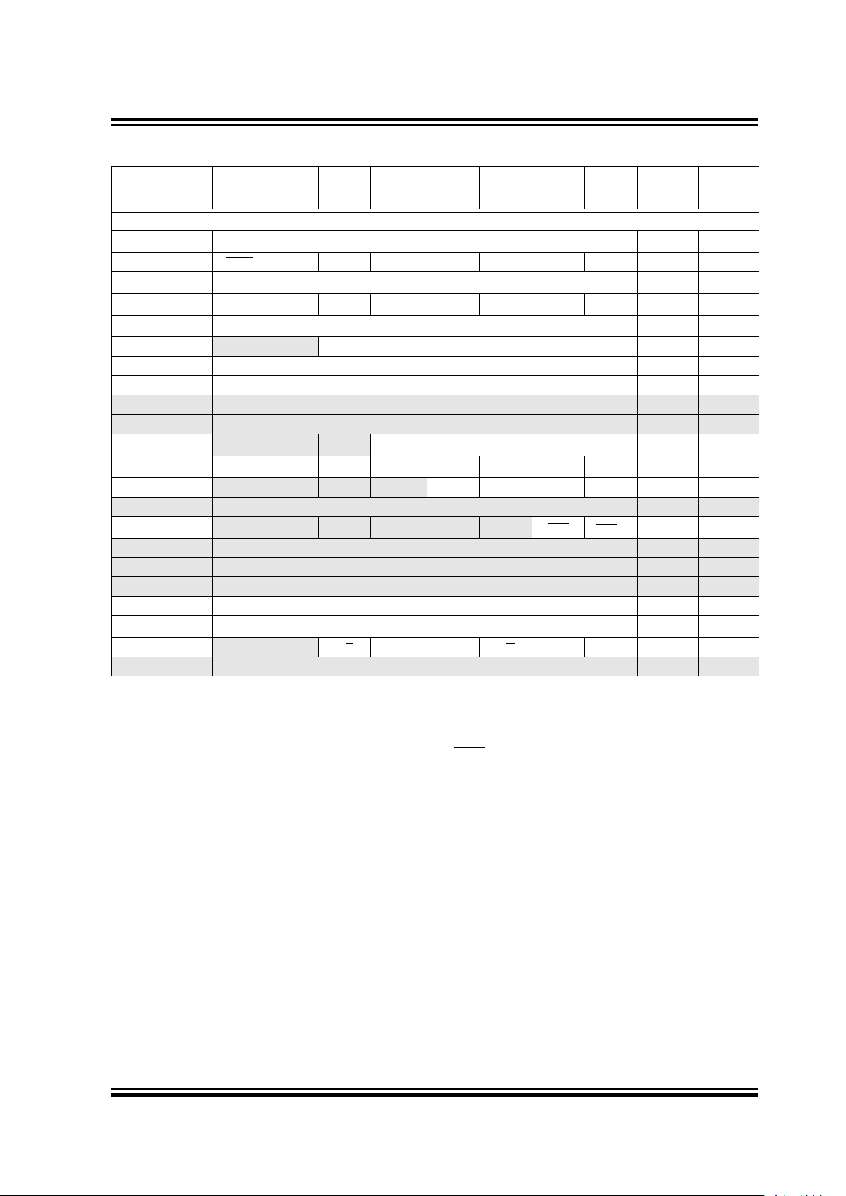
1997 Microchip Technology Inc. DS30234D-page 25
PIC16C6X
Bank 1
80h
(1)
INDF Addressing this location uses contents of FSR to address data memory (not a physical register) 0000 0000 0000 0000
81h OPTION RBPU
INTEDG T0CS T0SE PSA PS2 PS1 PS0 1111 1111 1111 1111
82h
(1)
PCL Program Counter's (PC) Least Significant Byte 0000 0000 0000 0000
83h
(1)
STATUS
IRP
(5)
RP1
(5)
RP0 TO PD ZDCC0001 1xxx 000q quuu
84h
(1)
FSR Indirect data memory address pointer xxxx xxxx uuuu uuuu
85h TRISA
— — PORTA Data Direction Register --11 1111 --11 1111
86h TRISB PORTB Data Direction Register 1111 1111 1111 1111
87h TRISC PORTC Data Direction Register 1111 1111 1111 1111
88h — Unimplemented — —
89h — Unimplemented — —
8Ah
(1,2)
PCLATH — — —
Write Buffer for the upper 5 bits of the Program Counter
---0 0000 ---0 0000
8Bh
(1)
INTCON GIE PEIE T0IE INTE RBIE T0IF INTF RBIF 0000 000x 0000 000u
8Ch PIE1
(6) (6) — — SSPIE CCP1IE TMR2IE TMR1IE 00-- 0000 00-- 0000
8Dh — Unimplemented — —
8Eh PCON
— — — — — — POR
BOR
(4)
---- --qq ---- --uu
8Fh — Unimplemented — —
90h — Unimplemented — —
91h — Unimplemented — —
92h PR2 Timer2 Period Register 1111 1111 1111 1111
93h SSPADD
Synchronous Serial Port (I
2
C mode) Address Register
0000 0000 0000 0000
94h SSPSTAT — — D/A P S R/W UA BF --00 0000 --00 0000
95h-9Fh — Unimplemented — —
TABLE 4-2: SPECIAL FUNCTION REGISTERS FOR THE PIC16C62/62A/R62 (Cont.’d)
Address Name Bit 7 Bit 6 Bit 5 Bit 4 Bit 3 Bit 2 Bit 1 Bit 0
Value on:
POR,
BOR
Value on
all other
resets
(3)
Legend: x = unknown, u = unchanged, q = value depends on condition, - = unimplemented location read as '0'.
Shaded locations are unimplemented, read as ‘0’.
Note 1: These registers can be addressed from either bank.
2: The upper byte of the Program Counter (PC) is not directly accessible. PCLATH is a holding register for the PC whose
contents are transferred to the upper byte of the program counter. (PC<12:8>)
3: Other (non power-up) resets include external reset through MCLR
and the Watchdog Timer reset.
4: The BOR bit is reserved on the PIC16C62, always maintain this bit set.
5: The IRP and RP1 bits are reserved on the PIC16C62/62A/R62, always maintain these bits clear.
6: PIE1<7:6> and PIR1<7:6> are reserved on the PIC16C62/62A/R62, always maintain these bits clear.
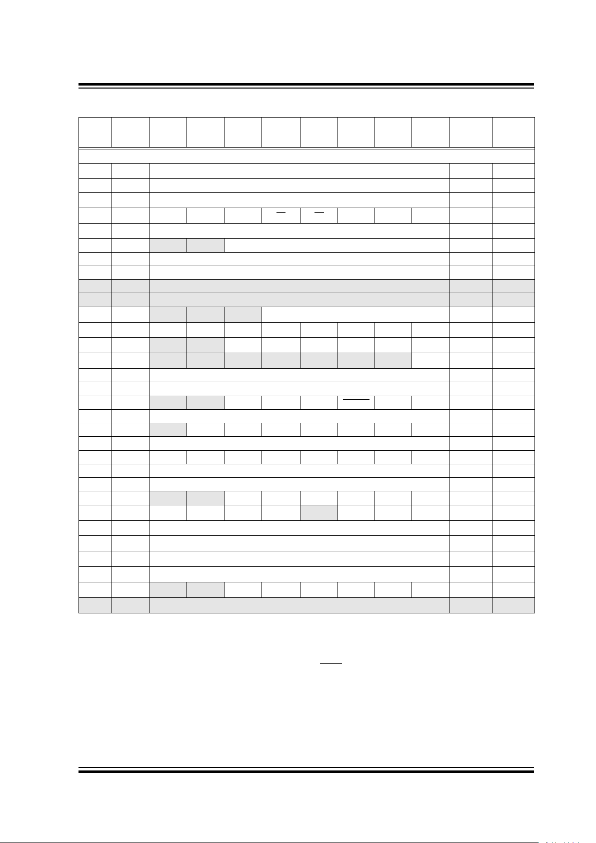
1997 Microchip Technology Inc. DS30234D-page 26
PIC16C6X
TABLE 4-3: SPECIAL FUNCTION REGISTERS FOR THE PIC16C63/R63
Address Name Bit 7 Bit 6 Bit 5 Bit 4 Bit 3 Bit 2 Bit 1 Bit 0
Value on:
POR,
BOR
Value on
all other
resets
(3)
Bank 0
00h
(1)
INDF Addressing this location uses contents of FSR to address data memory (not a physical register) 0000 0000 0000 0000
01h TMR0 Timer0 module’s register xxxx xxxx uuuu uuuu
02h
(1)
PCL Program Counter's (PC) Least Significant Byte 0000 0000 0000 0000
03h
(1)
STATUS
IRP
(4)
RP1
(4)
RP0 TO PD ZDCC0001 1xxx 000q quuu
04h
(1)
FSR Indirect data memory address pointer xxxx xxxx uuuu uuuu
05h PORTA
— — PORTA Data Latch when written: PORTA pins when read --xx xxxx --uu uuuu
06h PORTB PORTB Data Latch when written: PORTB pins when read xxxx xxxx uuuu uuuu
07h PORTC PORTC Data Latch when written: PORTC pins when read xxxx xxxx uuuu uuuu
08h — Unimplemented — —
09h — Unimplemented — —
0Ah
(1,2)
PCLATH — — —
Write Buffer for the upper 5 bits of the Program Counter
---0 0000 ---0 0000
0Bh
(1)
INTCON GIE PEIE T0IE INTE RBIE T0IF INTF RBIF 0000 000x 0000 000u
0Ch PIR1
(5) (5)
RCIF TXIF
SSPIF CCP1IF TMR2IF TMR1IF 0000 0000 0000 0000
0Dh PIR2
— — — —– — — — CCP2IF ---- ---0 ---- ---0
0Eh TMR1L Holding register for the Least Significant Byte of the 16-bit TMR1 register xxxx xxxx uuuu uuuu
0Fh TMR1H Holding register for the Most Significant Byte of the 16-bit TMR1 register xxxx xxxx uuuu uuuu
10h T1CON
— — T1CKPS1 T1CKPS0 T1OSCEN T1SYNC TMR1CS TMR1ON --00 0000 --uu uuuu
11h TMR2 Timer2 module’s register 0000 0000 0000 0000
12h T2CON — TOUTPS3 TOUTPS2 TOUTPS1 TOUTPS0 TMR2ON T2CKPS1 T2CKPS0 -000 0000 -000 0000
13h SSPBUF Synchronous Serial Port Receive Buffer/Transmit Register xxxx xxxx uuuu uuuu
14h SSPCON WCOL SSPOV SSPEN CKP SSPM3 SSPM2 SSPM1 SSPM0 0000 0000 0000 0000
15h CCPR1L Capture/Compare/PWM1 (LSB) xxxx xxxx uuuu uuuu
16h CCPR1H Capture/Compare/PWM1 (MSB) xxxx xxxx uuuu uuuu
17h CCP1CON — — CCP1X CCP1Y CCP1M3 CCP1M2 CCP1M1 CCP1M0 --00 0000 --00 0000
18h RCSTA
SPEN RX9 SREN CREN
— FERR OERR RX9D 0000 -00x 0000 -00x
19h TXREG
USART Transmit Data Register 0000 0000 0000 0000
1Ah RCREG
USART Receive Data Register 0000 0000 0000 0000
1Bh CCPR2L
Capture/Compare/PWM2 (LSB) xxxx xxxx uuuu uuuu
1Ch
CCPR2H
Capture/Compare/PWM2 (MSB) xxxx xxxx uuuu uuuu
1Dh
CCP2CON
— — CCP2X CCP2Y CCP2M3 CCP2M2 CCP2M1 CCP2M0 --00 0000 --00 0000
1Eh-1Fh
— Unimplemented
— —
Legend: x = unknown, u = unchanged, q = value depends on condition, - = unimplemented location read as '0'.
Shaded locations are unimplemented, read as ‘0’.
Note 1: These registers can be addressed from either bank.
2: The upper byte of the Program Counter (PC) is not directly accessible. PCLATH is a holding register for the PC whose
contents are transferred to the upper byte of the program counter. (PC<12:8>)
3: Other (non power-up) resets include external reset through MCLR and the Watchdog Timer reset.
4: The IRP and RP1 bits are reserved on the PIC16C63/R63, always maintain these bits clear.
5: PIE1<7:6> and PIR1<7:6> are reserved on the PIC16C63/R63, always maintain these bits clear.
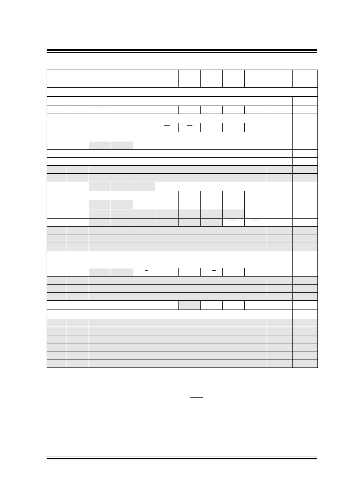
1997 Microchip Technology Inc. DS30234D-page 27
PIC16C6X
Bank 1
80h
(1)
INDF Addressing this location uses contents of FSR to address data memory (not a physical register) 0000 0000 0000 0000
81h OPTION RBPU
INTEDG T0CS T0SE PSA PS2 PS1 PS0 1111 1111 1111 1111
82h
(1)
PCL Program Counter's (PC) Least Significant Byte 0000 0000 0000 0000
83h
(1)
STATUS
IRP
(4)
RP1
(4)
RP0 TO PD ZDCC0001 1xxx 000q quuu
84h
(1)
FSR Indirect data memory address pointer xxxx xxxx uuuu uuuu
85h TRISA
— — PORTA Data Direction Register --11 1111 --11 1111
86h TRISB PORTB Data Direction Register 1111 1111 1111 1111
87h TRISC PORTC Data Direction Register 1111 1111 1111 1111
88h — Unimplemented — —
89h — Unimplemented — —
8Ah
(1,2)
PCLATH — — —
Write Buffer for the upper 5 bits of the Program Counter
---0 0000 ---0 0000
8Bh
(1)
INTCON GIE PEIE T0IE INTE RBIE T0IF INTF RBIF 0000 000x 0000 000u
8Ch PIE1
(5) (5)
RCIE TXIE
SSPIE CCP1IE TMR2IE TMR1IE 0000 0000 0000 0000
8Dh PIE2
— — — — — — — CCP2IE ---- ---0 ---- ---0
8Eh PCON
— — — — — — POR BOR ---- --qq ---- --uu
8Fh — Unimplemented — —
90h — Unimplemented — —
91h — Unimplemented — —
92h PR2 Timer2 Period Register 1111 1111 1111 1111
93h SSPADD
Synchronous Serial Port (I
2
C mode) Address Register
0000 0000 0000 0000
94h SSPSTAT — — D/A P S R/W UA BF --00 0000 --00 0000
95h — Unimplemented — —
96h — Unimplemented — —
97h — Unimplemented — —
98h
(2)
TXSTA CSRC TX9 TXEN SYNC — BRGH TRMT TX9D 0000 -010 0000 -010
99h
(2)
SPBRG Baud Rate Generator Register 0000 0000 0000 0000
9Ah — Unimplemented — —
9Bh — Unimplemented — —
9Ch — Unimplemented — —
9Dh — Unimplemented — —
9Eh — Unimplemented — —
9Fh — Unimplemented — —
TABLE 4-3: SPECIAL FUNCTION REGISTERS FOR THE PIC16C63/R63 (Cont.’d)
Address Name Bit 7 Bit 6 Bit 5 Bit 4 Bit 3 Bit 2 Bit 1 Bit 0
Value on:
POR,
BOR
Value on
all other
resets
(3)
Legend: x = unknown, u = unchanged, q = value depends on condition, - = unimplemented location read as '0'.
Shaded locations are unimplemented, read as ‘0’.
Note 1: These registers can be addressed from either bank.
2: The upper byte of the Program Counter (PC) is not directly accessible. PCLATH is a holding register for the PC whose
contents are transferred to the upper byte of the program counter. (PC<12:8>)
3: Other (non power-up) resets include external reset through MCLR and the Watchdog Timer reset.
4: The IRP and RP1 bits are reserved on the PIC16C63/R63, always maintain these bits clear.
5: PIE1<7:6> and PIR1<7:6> are reserved on the PIC16C63/R63, always maintain these bits clear.

PIC16C6X
DS30234D-page 28 1997 Microchip Technology Inc.
TABLE 4-4: SPECIAL FUNCTION REGISTERS FOR THE PIC16C64/64A/R64
Address Name Bit 7 Bit 6 Bit 5 Bit 4 Bit 3 Bit 2 Bit 1 Bit 0
Value on:
POR,
BOR
Value on
all other
resets
(3)
Bank 0
00h
(1)
INDF Addressing this location uses contents of FSR to address data memory (not a physical register) 0000 0000 0000 0000
01h TMR0 Timer0 module’s register xxxx xxxx uuuu uuuu
02h
(1)
PCL Program Counter's (PC) Least Significant Byte 0000 0000 0000 0000
03h
(1)
STATUS
IRP
(5)
RP1
(5)
RP0 TO PD ZDCC0001 1xxx 000q quuu
04h
(1)
FSR Indirect data memory address pointer xxxx xxxx uuuu uuuu
05h PORTA
— — PORTA Data Latch when written: PORTA pins when read --xx xxxx --uu uuuu
06h PORTB PORTB Data Latch when written: PORTB pins when read xxxx xxxx uuuu uuuu
07h PORTC PORTC Data Latch when written: PORTC pins when read xxxx xxxx uuuu uuuu
08h
PORTD
PORTD Data Latch when written: PORTD pins when read xxxx xxxx uuuu uuuu
09h
PORTE
— — — — — RE2 RE1 RE0 ---- -xxx ---- -uuu
0Ah
(1,2)
PCLATH — — —
Write Buffer for the upper 5 bits of the Program Counter
---0 0000 ---0 0000
0Bh
(1)
INTCON GIE PEIE T0IE INTE RBIE T0IF INTF RBIF 0000 000x 0000 000u
0Ch PIR1
PSPIF
(6) — — SSPIF CCP1IF TMR2IF TMR1IF 00-- 0000 00-- 0000
0Dh — Unimplemented — —
0Eh TMR1L Holding register for the Least Significant Byte of the 16-bit TMR1 register xxxx xxxx uuuu uuuu
0Fh TMR1H Holding register for the Most Significant Byte of the 16-bit TMR1 register xxxx xxxx uuuu uuuu
10h T1CON — — T1CKPS1 T1CKPS0 T1OSCEN T1SYNC TMR1CS TMR1ON --00 0000 --uu uuuu
11h TMR2 Timer2 module’s register 0000 0000 0000 0000
12h T2CON
— TOUTPS3 TOUTPS2 TOUTPS1 TOUTPS0 TMR2ON T2CKPS1 T2CKPS0 -000 0000 -000 0000
13h SSPBUF Synchronous Serial Port Receive Buffer/Transmit Register xxxx xxxx uuuu uuuu
14h SSPCON WCOL SSPOV SSPEN CKP SSPM3 SSPM2 SSPM1 SSPM0 0000 0000 0000 0000
15h CCPR1L Capture/Compare/PWM1 (LSB) xxxx xxxx uuuu uuuu
16h CCPR1H Capture/Compare/PWM1 (MSB) xxxx xxxx uuuu uuuu
17h CCP1CON — — CCP1X CCP1Y CCP1M3 CCP1M2 CCP1M1 CCP1M0 --00 0000 --00 0000
18h-1Fh
— Unimplemented
— —
Legend: x = unknown, u = unchanged, q = value depends on condition, - = unimplemented location read as '0'.
Shaded locations are unimplemented, read as ‘0’.
Note 1: These registers can be addressed from either bank.
2: The upper byte of the Program Counter (PC) is not directly accessible. PCLATH is a holding register for the PC whose
contents are transferred to the upper byte of the program counter. (PC<12:8>)
3: Other (non power-up) resets include external reset through MCLR and the Watchdog Timer reset.
4: The BOR bit is reserved on the PIC16C64, always maintain this bit set.
5: The IRP and RP1 bits are reserved on the PIC16C64/64A/R64, always maintain these bits clear.
6: PIE1<6> and PIR1<6> are reserved on the PIC16C64/64A/R64, always maintain these bits clear.
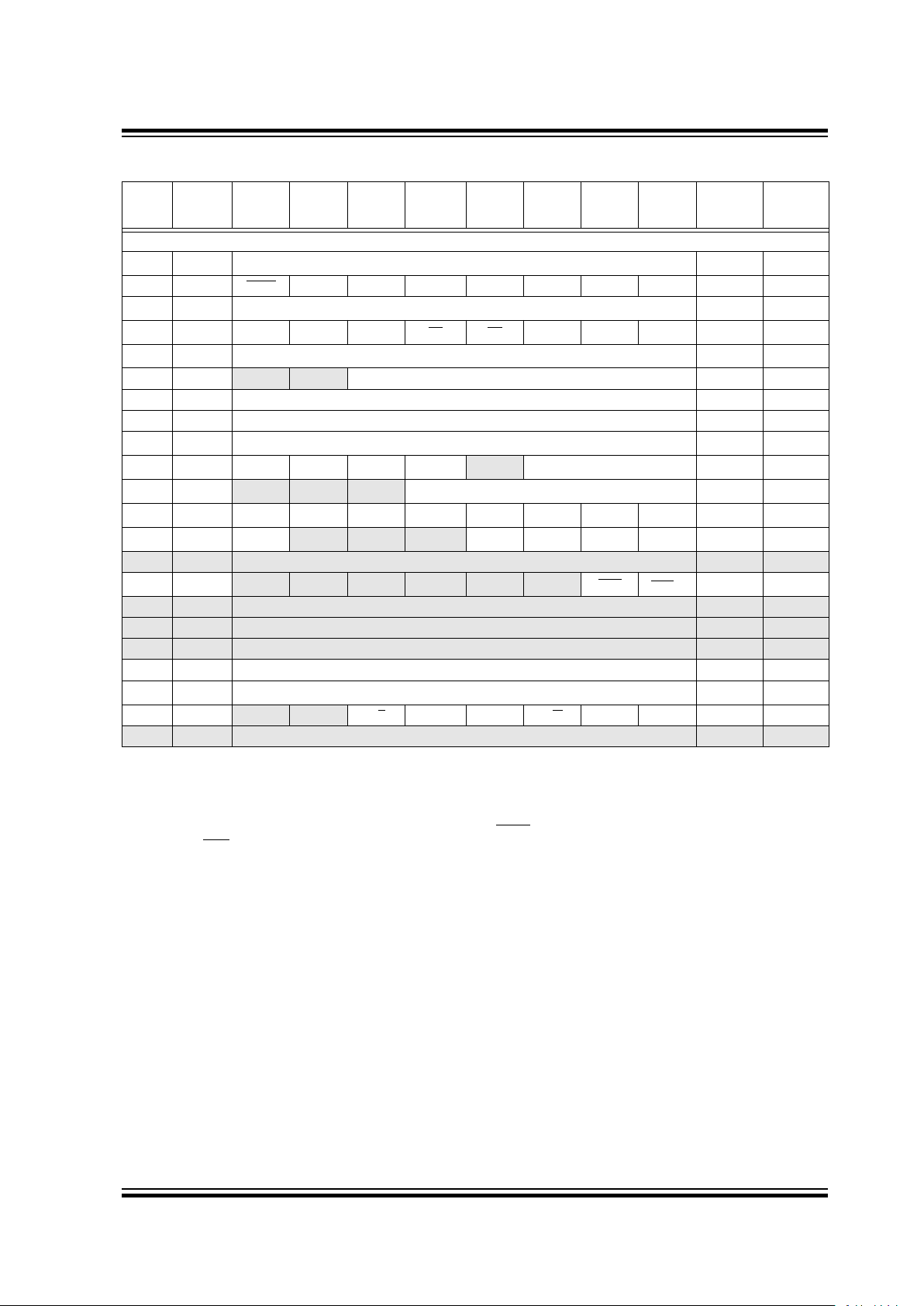
1997 Microchip Technology Inc. DS30234D-page 29
PIC16C6X
Bank 1
80h
(1)
INDF Addressing this location uses contents of FSR to address data memory (not a physical register) 0000 0000 0000 0000
81h OPTION RBPU
INTEDG T0CS T0SE PSA PS2 PS1 PS0 1111 1111 1111 1111
82h
(1)
PCL Program Counter's (PC) Least Significant Byte 0000 0000 0000 0000
83h
(1)
STATUS
IRP
(5)
RP1
(5)
RP0 TO PD ZDCC0001 1xxx 000q quuu
84h
(1)
FSR Indirect data memory address pointer xxxx xxxx uuuu uuuu
85h TRISA
— — PORTA Data Direction Register --11 1111 --11 1111
86h TRISB PORTB Data Direction Register 1111 1111 1111 1111
87h TRISC PORTC Data Direction Register 1111 1111 1111 1111
88h TRISD
PORTD Data Direction Register 1111 1111 1111 1111
89h TRISE
IBF OBF IBOV PSPMODE
— PORTE Data Direction Bits 0000 -111 0000 -111
8Ah
(1,2)
PCLATH — — —
Write Buffer for the upper 5 bits of the Program Counter
---0 0000 ---0 0000
8Bh
(1)
INTCON GIE PEIE T0IE INTE RBIE T0IF INTF RBIF 0000 000x 0000 000u
8Ch PIE1
PSPIE
(6) — — SSPIE CCP1IE TMR2IE TMR1IE 00-- 0000 00-- 0000
8Dh — Unimplemented — —
8Eh PCON
— — — — — — POR
BOR
(4)
---- --qq ---- --uu
8Fh — Unimplemented — —
90h — Unimplemented — —
91h — Unimplemented — —
92h PR2 Timer2 Period Register 1111 1111 1111 1111
93h SSPADD
Synchronous Serial Port (I
2
C mode) Address Register
0000 0000 0000 0000
94h SSPSTAT — — D/A P S R/W UA BF --00 0000 --00 0000
95h-9Fh — Unimplemented — —
TABLE 4-4: SPECIAL FUNCTION REGISTERS FOR THE PIC16C64/64A/R64 (Cont.’d)
Address Name Bit 7 Bit 6 Bit 5 Bit 4 Bit 3 Bit 2 Bit 1 Bit 0
Value on:
POR,
BOR
Value on
all other
resets
(3)
Legend: x = unknown, u = unchanged, q = value depends on condition, - = unimplemented location read as '0'.
Shaded locations are unimplemented, read as ‘0’.
Note 1: These registers can be addressed from either bank.
2: The upper byte of the Program Counter (PC) is not directly accessible. PCLATH is a holding register for the PC whose
contents are transferred to the upper byte of the program counter. (PC<12:8>)
3: Other (non power-up) resets include external reset through MCLR and the Watchdog Timer reset.
4: The BOR bit is reserved on the PIC16C64, always maintain this bit set.
5: The IRP and RP1 bits are reserved on the PIC16C64/64A/R64, always maintain these bits clear.
6: PIE1<6> and PIR1<6> are reserved on the PIC16C64/64A/R64, always maintain these bits clear.
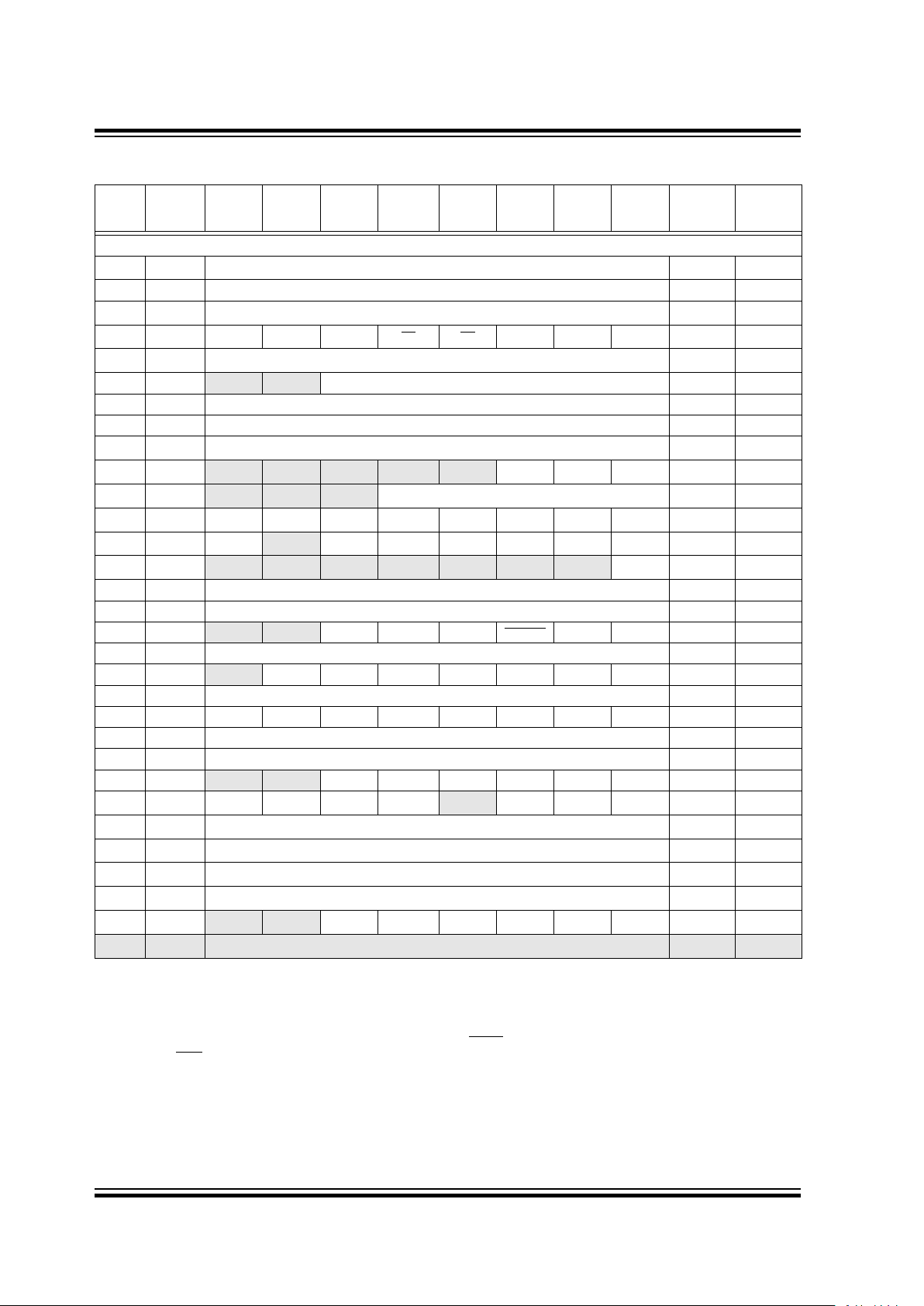
PIC16C6X
DS30234D-page 30 1997 Microchip Technology Inc.
TABLE 4-5: SPECIAL FUNCTION REGISTERS FOR THE PIC16C65/65A/R65
Address Name Bit 7 Bit 6 Bit 5 Bit 4 Bit 3 Bit 2 Bit 1 Bit 0
Value on:
POR,
BOR
Value on
all other
resets
(3)
Bank 0
00h
(1)
INDF Addressing this location uses contents of FSR to address data memory (not a physical register) 0000 0000 0000 0000
01h TMR0 Timer0 module’s register xxxx xxxx uuuu uuuu
02h
(1)
PCL Program Counter's (PC) Least Significant Byte 0000 0000 0000 0000
03h
(1)
STATUS
IRP
(5)
RP1
(5)
RP0 TO PD ZDCC0001 1xxx 000q quuu
04h
(1)
FSR Indirect data memory address pointer xxxx xxxx uuuu uuuu
05h PORTA
— — PORTA Data Latch when written: PORTA pins when read --xx xxxx --uu uuuu
06h PORTB PORTB Data Latch when written: PORTB pins when read xxxx xxxx uuuu uuuu
07h PORTC PORTC Data Latch when written: PORTC pins when read xxxx xxxx uuuu uuuu
08h
PORTD
PORTD Data Latch when written: PORTD pins when read xxxx xxxx uuuu uuuu
09h
PORTE
— — — — — RE2 RE1 RE0 ---- -xxx ---- -uuu
0Ah
(1,2)
PCLATH — — —
Write Buffer for the upper 5 bits of the Program Counter
---0 0000 ---0 0000
0Bh
(1)
INTCON GIE PEIE T0IE INTE RBIE T0IF INTF RBIF 0000 000x 0000 000u
0Ch PIR1
PSPIF
(6)
RCIF TXIF
SSPIF CCP1IF TMR2IF TMR1IF 0000 0000 0000 0000
0Dh PIR2
— — — —– — — — CCP2IF ---- ---0 ---- ---0
0Eh TMR1L Holding register for the Least Significant Byte of the 16-bit TMR1 register xxxx xxxx uuuu uuuu
0Fh TMR1H Holding register for the Most Significant Byte of the 16-bit TMR1 register xxxx xxxx uuuu uuuu
10h T1CON
— — T1CKPS1 T1CKPS0 T1OSCEN T1SYNC TMR1CS TMR1ON --00 0000 --uu uuuu
11h TMR2 Timer2 module’s register 0000 0000 0000 0000
12h T2CON — TOUTPS3 TOUTPS2 TOUTPS1 TOUTPS0 TMR2ON T2CKPS1 T2CKPS0 -000 0000 -000 0000
13h SSPBUF Synchronous Serial Port Receive Buffer/Transmit Register xxxx xxxx uuuu uuuu
14h SSPCON WCOL SSPOV SSPEN CKP SSPM3 SSPM2 SSPM1 SSPM0 0000 0000 0000 0000
15h CCPR1L Capture/Compare/PWM1 (LSB) xxxx xxxx uuuu uuuu
16h CCPR1H Capture/Compare/PWM1 (MSB) xxxx xxxx uuuu uuuu
17h CCP1CON — — CCP1X CCP1Y CCP1M3 CCP1M2 CCP1M1 CCP1M0 --00 0000 --00 0000
18h RCSTA
SPEN RX9 SREN CREN
— FERR OERR RX9D 0000 -00x 0000 -00x
19h TXREG
USART Transmit Data Register 0000 0000 0000 0000
1Ah RCREG
USART Receive Data Register 0000 0000 0000 0000
1Bh CCPR2L
Capture/Compare/PWM2 (LSB) xxxx xxxx uuuu uuuu
1Ch
CCPR2H
Capture/Compare/PWM2 (MSB) xxxx xxxx uuuu uuuu
1Dh
CCP2CON
— — CCP2X CCP2Y CCP2M3 CCP2M2 CCP2M1 CCP2M0 --00 0000 --00 0000
1Eh-1Fh
— Unimplemented
— —
Legend: x = unknown, u = unchanged, q = value depends on condition, - = unimplemented location read as '0'.
Shaded locations are unimplemented, read as ‘0’.
Note 1: These registers can be addressed from either bank.
2: The upper byte of the Program Counter (PC) is not directly accessible. PCLATH is a holding register for the PC whose
contents are transferred to the upper byte of the program counter. (PC<12:8>)
3: Other (non power-up) resets include external reset through MCLR and the Watchdog Timer reset.
4: The BOR bit is reserved on the PIC16C65, always maintain this bit set.
5: The IRP and RP1 bits are reserved on the PIC16C65/65A/R65, always maintain these bits clear.
6: PIE1<6> and PIR1<6> are reserved on the PIC16C65/65A/R65, always maintain these bits clear.
 Loading...