


PIC12CE673-04-JW
Table of contents
 Loading...
Microchip Technology Inc PIC12CE673-04-JW, PIC12CE673-04-P, PIC12CE673-04E-JW, PIC12CE674-04-P, PIC12CE674-04E-JW Datasheet
...
M
PIC12CE67X
8-Pin, 8-Bit CMOS Microcontroller with A/D Converter
and EEPROM Data Memory
Devices:
PIC12CE673 and PIC12CE674 are 8-bit OTP microcontrollers with 8-bit A/D Converter and EEPROM data
memory packaged in 8-lead packages. They are based
on the 14-bit PICmicro™ MCU architecture.
High-Performance RISC CPU:
• Only 35 single word instructions to learn
• All instructions are single cycle (400 ns) except for
program branches which are two-cycle
• Operating speed: DC - 10 MHz clock input
Device
PIC12CE673 1024 x 14 128 x 8 16 x 8
PIC12CE674 2048 x 14 128 x 8 16 x 8
• 14-bit wide instructions
• 8-bit wide data path
• Interrupt capability
• Special function hardware registers
• 8-level deep hardware stack
• Direct, indirect and relative addressing modes for
data and instructions
DC - 400 ns instruction cycle
Memory
Program
Data
RAM
Data
EEPROM
Peripheral Features:
• 8-bit real time clock/counter (TMR0) with 8-bit
programmable prescaler
• Interrupt on pin change (GP0, GP1, GP3)
• 1,000,000 erase/write cycle EEPROM data
memory
• EEPROM data retention > 40 years
• Four-channel, 8-bit A/D converter
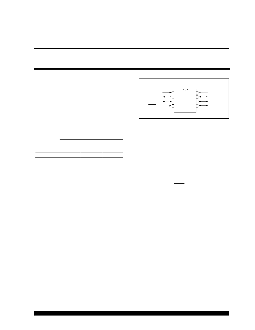
Pin Diagram:
PDIP , Windo wed CERDIP
PIC12CE673
CLKOUT
GP3/MCLR
VDD
/VPP
GP5/OSC1/CLKIN
GP4/OSC2/AN3/
PIC12CE674
1
2
3
4
VSS
8
GP0/AN0
7
GP1/AN1/V
6
5
GP2/T0CKI/
AN2/INT
Special Microcontroller Features:
• In-Circuit Serial Programming (ICSP™)
• Internal 4 MHz oscillator with programmable
calibration
• Selectable clockout
• Power-on Reset (POR)
• Power-up Timer (PWRT) and Oscillator Start-up
Timer (OST)
• Watchdog Timer (WDT) with its own on-chip RC
oscillator for reliable operation
• Programmable code protection
• Power saving SLEEP mode
• Internal pull-ups on I/O pins (GP0, GP1)
• Internal pull-up on MCLR
• Selectable oscillator options:
- INTRC: Precision internal 4 MHz oscillator
- EXTRC: External low-cost RC oscillator
- XT: Standard crystal/resonator
- HS: High speed crystal/resonator
- LP: Power saving, low frequency crystal
pin
CMOS Technology:
• Low-power, high-speed CMOS EPROM/
EEPROM technology
• Fully static design
• Wide operating voltage range 2.5V to 5.5V
• Commercial, Industrial, and Extended
temperature ranges
• Low power consumption
< 2 mA @ 5V, 4 MHz
15 µA typical @ 3V, 32 kHz
< 1 µA typical standby current
REF
1998 Microchip Technology Inc.
Preliminary
DS40181A-page 1

PIC12CE67X
Table of Contents
1.0 General Description....................................................................................................................................................................... 3
2.0 PIC12CE67X Device Varieties....................................................................................................................................................... 5
3.0 Architectural Overview...................................................................................................................................................................7
4.0 Memory Organization................................................................................................................................................................... 11
5.0 I/O Port......................................................................................................................................................................................... 25
6.0 EEPROM Peripheral Operation................................................................................................................................................... 27
7.0 Timer0 Module.............................................................................................................................................................................31
8.0 Analog-to-Digital Converter (A/D) Module ................................................................................................................................... 37
9.0 Special Features of the CPU ....................................................................................................................................................... 45
10.0 Instruction Set Summary..............................................................................................................................................................61
11.0 Development Support .................................................................................................................................................................. 75
12.0 Electrical Characteristics for PIC12CE67X .................................................................................................................................. 79
13.0 DC and AC Characteristics - PIC12CE67X ................................................................................................................................. 95
14.0 Packaging Information ............................................................................................................................................................... 101
Appendix A: Code for Accessing EEPROM Data Memory ............................................................................................................ 105
Index .................................................................................................................................................................................................. 107
On-Line Support................................................................................................................................................................................. 111
PIC12CE67X Product Identification System ..................................................................................................................................... 113
To Our Valued Customers
We constantly strive to improve the quality of all our products and documentation. We have spent an exceptional
amount of time to ensure that these documents are correct. However, we realize that we may have missed a few
things. If you find any information that is missing or appears in error, please use the reader response form in the
back of this data sheet to inform us. We appreciate your assistance in making this a better document.
DS40181A-page 2
Preliminary
1998 Microchip Technology Inc.

PIC12CE67X
1.0 GENERAL DESCRIPTION
The PIC12CE67X devices are low-cost, high-performance, CMOS, fully-static, 8-bit microcontroller with
integrated analog-to-digital (A/D) converter and
EEPROM data memory in the PIC12CEXXX Microcontroller family.
All PICmicro™ microcontrollers employ an advanced
RISC architecture. The PIC12CE67X microcontrollers
have enhanced core features, eight-level deep stack,
and multiple internal and external interrupt sources.
The separate instruction and data buses of the Harvard
architecture allow a 14-bit wide instruction word with
the separate 8-bit wide data. The two stage instruction
pipeline allows all instructions to execute in a single
cycle, except for program branches which require two
cycles. A total of 35 instructions (reduced instruction
set) are available. Additionally, a large register set gives
some of the architectural innovations used to achiev e a
very high performance.
PIC12CE67X microcontrollers typically achieve a 2:1
code compression and a 4:1 speed improvement over
other 8-bit microcontrollers in their class.
The PIC12CE67X devices ha ve 128 b ytes of RAM, 16
bytes of EEPROM data memory, 5 I/O
pin. In addition a timer/counter is available. Also a 4channel high-speed 8-bit A/D is provided. The 8-bit resolution is ideally suited for applications requiring lowcost analog interface, e.g. thermostat control, pressure
sensing, etc.
The PIC12CE67X device has special features to
reduce external components, thus reducing cost,
enhancing system reliability and reducing power consumption. The PIC12CE67X products are equipped
with special features that reduce system cost and
power requirements. The Power-On Reset (POR),
Power-up Timer (PWRT), and Oscillator Start-up Timer
(OST) eliminate the need for external reset circuitry.
There are five oscillator configurations to choose from,
including INTRC precision internal oscillator mode and
the power-saving LP (Low Power) oscillator. Power
saving SLEEP mode, Watchdog Timer and code
protection features improve system cost, power and
reliability.The SLEEP (power-down) feature provides a
power saving mode. The user can wake up the chip
from SLEEP through several external and internal
interrupts and resets.
pins and 1 input
A highly reliable Watchdog Timer with its own on-chip
RC oscillator provides protection against software lockup.
A UV erasable windowed package version is ideal for
code development while the cost-effective One-TimeProgrammable (OTP) version is suitable for production
in any volume. The customer can take full advantage of
Microchip’s price leadership in OTP microcontrollers
while benefiting from the OTP’s flexibility.
The PIC12CE67X device fits perfectly in applications
ranging from security and remote sensors to appliance
control and automotive. The EPROM technology
makes customization of application programs (transmitter codes, motor speeds, receiver frequencies, etc.)
extremely fast and convenient. The small footprint
packages make this microcontroller series perfect for
all applications with space limitations. Low cost, low
power, high perf ormance, ease of use and I/O flexibility
make the PIC12CE67X very versatile even in areas
where no microcontroller use has been considered
before (e.g. timer functions, communications and
coprocessor applications).
1.1 F
The PIC12CE67X products are compatible with other
members of the 14-Bit, PIC12C67X and PIC16CXXX
families.
1.2 De
The PIC12CE67X device is supported by a full-featured macro assembler, a software simulator, an in-circuit emulator, a low-cost de velopment prog rammer and
a full-featured programmer. A “C” compiler and fuzzy
logic support tools are also available.
amily and Upward Compatibility
velopment Support
1998 Microchip Technology Inc.
Preliminary
DS40181A-page 3

PIC12CE67X
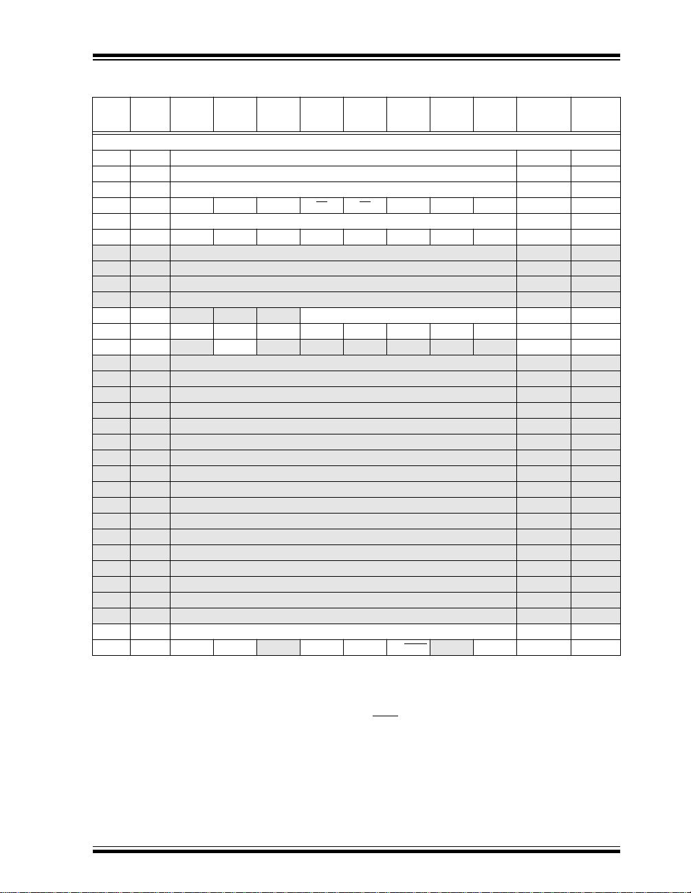
TABLE 1-1: PIC12CXXX & PIC12CEXXX FAMILY OF DEVICES
Clock
Memory
Peripherals
Features
PIC12C508(A)
Maximum
Frequency
of Operation
(MHz)
EPROM
Program
Memory
RAM Data
Memory
(bytes)
EEPROM
Data Memory
(bytes)
Timer
Module(s)
A/D Converter (8-bit)
Channels
Wake-up
from SLEEP
on pin
change
Interrupt
Sources
I/O Pins 5 5 5 5 5 5 5 5
Input Pins 1 1 1 1 1 1 1 1
Internal
Pull-ups
In-Circuit
Serial
Programming
Number of
Instructions
Packages 8-pin DIP,
4 4 4 4 10 10 10 10
512 x 12 1024 x 12 512 x 12 1024 x 12 1024 x 14 2048 x 14 1024 x 14 2048 x 14
25 41 25 41 128 128
— — 16 16 — —
TMR0 TMR0 TMR0 TMR0 TMR0 TMR0 TMR0 TMR0
— — — — 4 4 4 4
Yes Yes Yes Yes Yes Yes Yes Yes
— — 4 4 4 4
Yes Yes Yes Yes Yes Yes Yes Yes
Yes Yes Yes Yes Yes Yes Yes Yes
33 33 33 33 35 35 35 35
JW, SOIC
PIC12C509(A) PIC12CE518 PIC12CE519 PIC12C671 PIC12C672 PIC12CE673 PIC12CE674
8-pin DIP,
JW, SOIC
8-pin DIP,
JW, SOIC
8-pin DIP,
JW, SOIC
8-pin DIP,
JW, SOIC
8-pin DIP,
JW, SOIC
128 128
16 16
8-pin DIP, JW8-pin DIP,
JW
All PIC12CXXX & PIC12CEXXX devices have Power-on Reset, selectable Watchdog Timer, selectable
code protect and high I/O current capability.
All PIC12CXXX & PIC12CEXXX devices use serial programming with data pin GP0 and clock pin GP1.
DS40181A-page 4
Preliminary
1998 Microchip Technology Inc.

PIC12CE67X
2.0 PIC12CE67X DEVICE
VARIETIES
A variety of frequency ranges and packaging options
are available. Depending on application and production
requirements, the proper device option can be selected
using the information in the PIC12CE67X Product
Identification System section at the end of this data
sheet. When placing orders, please use that page of
the data sheet to specify the correct part number.
For the PIC12CE67X, the device “type” is indicated in
the device number:
1.CE, as in PIC12CE671. These devices have
OTP program memory, EEPROM data memory
and operate over the standard voltage range.
2.1 UV Erasab
The UV erasable version, offered in windowed package, is optimal for prototype dev elopment and pilot programs.
The UV erasable version can be erased and reprogrammed to any of the configuration modes.
Microchip's PICSTART Plus and PRO MATE programmers both support the PIC12CE67X. Third party
programmers also are available; refer to the Microchip
Third Party Guide for a list of sources.
Note:
Please note that erasing the device will
also erase the pre-programmed internal
calibration value for the internal oscillator.
The calibration value must be saved prior
to erasing the part.
2.2 One-Time-Pr
Devices
The availability of OTP devices is especially useful for
customers who need the flexibility for frequent code
updates and small volume applications.
The OTP devices, packaged in plastic packages, permit the user to program them once. In addition to the
program memory, the configuration bits must also be
programmed.
le Devices
ogrammable (OTP)
2.3 Quic
k-Turn-Programming (QTP)
Devices
Microchip offers a QTP Programming Service for factory production orders. This service is made available
for users who choose not to program a medium to high
quantity of units and whose code patterns have stabilized. The devices are identical to the OTP devices but
with all EPROM locations and configuration options
already programmed by the factory. Certain code and
prototype verification procedures apply before production shipments are available. Please contact your local
Microchip Technology sales office for more details.
2.4 Serializ
Microchip offers a unique programming service where
a few user-defined locations in each device are programmed with different serial numbers. The serial numbers may be random, pseudo-random, or sequential.
Serial programming allows each device to have a
unique number which can serve as an entry-code,
password, or ID number.
ed Quick-Turn Programming
SM
(SQTP
Devices
)
1998 Microchip Technology Inc.
Preliminary
DS40181A-page 5

PIC12CE67X
NOTES:
DS40181A-page 6
Preliminary
1998 Microchip Technology Inc.

PIC12CE67X
3.0 ARCHITECTURAL OVERVIEW
The high performance of the PIC12CE67X family can
be attributed to a number of architectural features commonly found in RISC microprocessors. To begin with,
the PIC12CE67X uses a Harvard architecture, in which
program and data are accessed from separate memories using separate buses. This improves bandwidth
over traditional von Neumann architecture in which program and data are fetched from the same memory
using the same bus. Separating program and data
buses also allow instructions to be sized differently than
the 8-bit wide data word. Instruction opcodes are 14bits wide making it possible to have all single word
instructions. A 14-bit wide program memory access
bus fetches a 14-bit instruction in a single cycle. A twostage pipeline overlaps fetch and execution of instructions (Example 3-1). Consequently, all instructions (35)
execute in a single cycle (1 µs @ 4 MHz) except for program branches.
The table below lists program memory (EPROM), data
memory (RAM), and non-volatile memory (EEPROM)
for each PIC12CE67X device.
Device
PIC12CE673 1K x 14 128 x 8 16x8
PIC12CE674 2K x 14 128 x 8 16x8
Program
Memory
RAM
Data
Memory
EEPROM
Data
Memory
The PIC12CE67X can directly or indirectly address its
register files or data memory. All special function registers, including the program counter, are mapped in the
data memory. The PIC12CE67X has an orthogonal
(symmetrical) instruction set that makes it possible to
carry out any operation on any register using any
addressing mode. This symmetrical nature and lack of
‘special optimal situations’ mak e prog r amming with the
PIC12CE67X simple yet efficient. In addition, the learning curve is reduced significantly.
PIC12CE67X devices contain an 8-bit ALU and working register. The ALU is a general purpose arithmetic
unit. It performs arithmetic and Boolean functions
between the data in the working register and any register file.
The ALU is 8-bits wide and capable of addition, subtraction, shift and logical operations. Unless otherwise
mentioned, arithmetic operations are two's complement in nature. In two-operand instructions, typically
one operand is the working register (W register). The
other operand is a file register or an immediate constant. In single operand instructions, the operand is
either the W register or a file register.
The W register is an 8-bit working register used for ALU
operations. It is not an addressable register.
Depending on the instruction executed, the ALU may
affect the values of the Carry (C), Digit Carry (DC), and
Zero (Z) bits in the ST ATUS register. The C and DC bits
operate as a borro
respectively, in subtraction. See the
instructions for examples.
w bit and a digit borrow out bit,
SUBLW
and
SUBWF
1998 Microchip Technology Inc.
Preliminary
DS40181A-page 7
PIC12CE67X
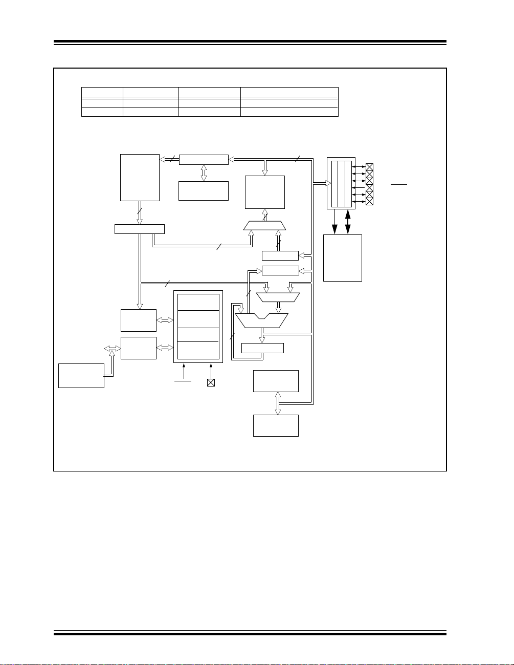
FIGURE 3-1: PIC12CE67X BLOCK DIAGRAM
PIC12CE673
PIC12CE674
OSC1/CLKIN
OSC2/CLKOUT
Internal
4 MHz Clock
Device
Program
Bus
Program Memory Data Memory (RAM)
1K x 14
2K x 14
EPROM
Program
Memory
14
Instruction reg
Instruction
Decode &
Control
Timing
Generation
8
13
Program Counter
8 Level Stack
Direct Addr
Power-up
Timer
Oscillator
Start-up Timer
Watchdog
Timer
Power-on
Reset
MCLR
128 x 8
128 x 8
(13 bit)
VDD, VSS
Non-Volatile Memory (EEPROM)
Data Bus
RAM
128 bytes
File
Registers
(1)
RAM Addr
7
8
3
9
Addr MUX
8
FSR reg
STATUS reg
MUX
ALU
W reg
Timer0
16 x 8
16 x 8
Indirect
Addr
8
GPIO
SCL
16x8
EEPROM
Data
Memory
GP0/AN0
GP1/AN1/VREF
GP2/T0CKI/AN2/INT
GP3/MCLR/Vpp
GP4/OSC2/AN3/CLKOUT
GP5/OSC1/CLKIN
SDA
Note 1: Higher order bits are from the STATUS register.
DS40181A-page 8
Preliminary
A/D
1998 Microchip Technology Inc.

PIC12CE67X
TABLE 3-1: PIC12CE67X PINOUT DESCRIPTION
DIP
Name
GP0/AN0 7 7 I/O TTL/ST Bi-directional I/O port/serial programming data/analog
GP1/AN1/V
GP2/T0CKI/AN2/INT 5 5 I/O ST Bi-directional I/O port/analog input 2. Can be config-
GP3/MCLR
GP4/OSC2/AN3/
CLKOUT
GP5/OSC1/CLKIN 2 2 I/O TTL/ST Bidirectional IO port oscillator crystal input/external
V
DD
SS
V
REF
/V
PP
Legend: I = input, O = output, I/O = input/output, P = power, — = not used, TTL = TTL input,
ST = Schmitt Trigger input
Pin #
SOIC
Pin #
6 6 I/O TTL/ST Bi-directional I/O port/serial programming clock/analog
4 4 I TTL Input port/master clear (reset) input/programming volt-
3 3 I/O TTL Bi-directional I/O port/oscillator crystal output/analog
1 1 P — Positive supply for logic and I/O pins
8 8 P — Ground reference for logic and I/O pins
I/O/P
Type
Buffer
Type
Description
input 0. Can be software programmed for internal
weak pull-up and interrupt on pin change. This b uffer is
a Schmitt Trigger input when used in serial programming mode.
input 1/voltage reference. Can be software programmed for internal weak pull-up and interrupt on pin
change. This buffer is a Schmitt Trigger input when
used in serial programming mode.
ured as T0CKI or external interrupt.
age input. When configured as MCLR
active low reset to the device. Voltage on MCLR
must not exceed VDD during normal device operation.
Can be software programmed for internal weak pull-up
and interrupt on pin change. W eak pull-up alw ays on if
configured as MCLR
input 3. Connections to crystal or resonator in crystal
oscillator mode (XT and LP modes only , GPIO in other
modes). In EXTRC and INTRC modes, the pin output
can be configured to CLKOUT which has 1/4 the frequency of OSC1 and denotes the instruction cycle
rate.
clock source input (GPIO in INTRC mode only, OSC1
in all other oscillator modes). Schmitt trigger in EXTRC
mode only.
.
, this pin is an
/V
PP
1998 Microchip Technology Inc.
Preliminary
DS40181A-page 9
PIC12CE67X
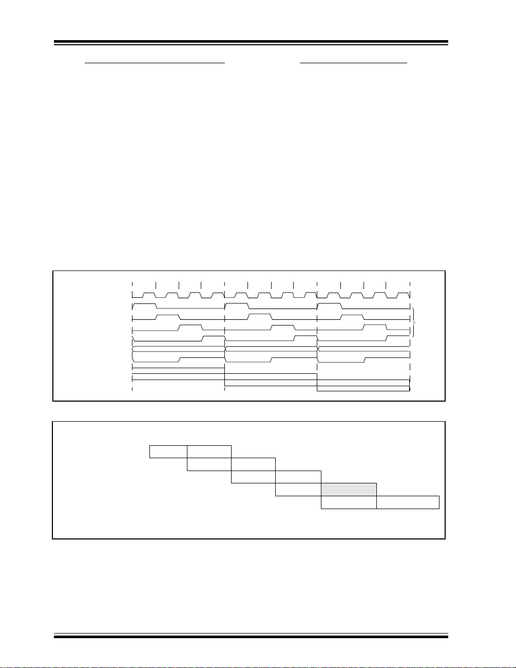
3.1 Cloc
king Scheme/Instruction Cycle
The clock input (from OSC1) is internally divided by
four to generate four non-overlapping quadrature
clocks namely Q1, Q2, Q3 and Q4. Internally, the program counter (PC) is incremented every Q1, the
instruction is fetched from the program memory and
latched into the instruction register in Q4. The instruction is decoded and executed during the following Q1
through Q4. The clocks and instruction execution flow
is shown in Figure 3-2.
FIGURE 3-2: CLOCK/INSTRUCTION CYCLE
Q2 Q3 Q4
Q1
OSC1
Q1
Q2
Q3
Q4
PC
OSC2/CLKOUT
(EXTRC and
INTRC modes)
PC PC+1 PC+2
Fetch INST (PC)
Execute INST (PC-1) Fetch INST (PC+1)
3.2 Instruction Flo
An “Instruction Cycle” consists of four Q cycles (Q1,
Q2, Q3 and Q4). The instruction fetch and execute
are pipelined such that fetch takes one instruction
cycle while decode and execute takes another
instruction cycle. However, due to the pipelining,
each instruction effectively executes in one cycle. If
an instruction causes the program counter to change
(e.g.
GOTO
the instruction (Example 3-1).
A fetch cycle begins with the program counter (PC)
incrementing in Q1.
In the execution cycle, the fetched instruction is
latched into the “Instruction Register" (IR) in cycle
Q1. This instruction is then decoded and executed
during the Q2, Q3, and Q4 cycles. Data memory is
read during Q2 (operand read) and written during Q4
(destination write).
Q2 Q3 Q4
Q1
Execute INST (PC) Fetch INST (PC+2)
) then two cycles are required to complete
Q1
Execute INST (PC+1)
w/Pipelining
Q2 Q3 Q4
Internal
phase
clock
EXAMPLE 3-1: INSTRUCTION PIPELINE FLOW
Tcy0 Tcy1 Tcy2 Tcy3 Tcy4 Tcy5
1. MOVLW 55h
2. MOVWF GPIO
3. CALL SUB_1
4. BSF GPIO, BIT3 (Forced NOP)
5. Instruction @ address SUB_1
All instructions are single cycle, except for any progr am branches . These take two cycles since the fetch instruction is “flushed” from the pipeline while the new instruction is being fetched and then executed.
DS40181A-page 10
Fetch 1 Execute 1
Fetch 2 Execute 2
Fetch 3 Execute 3
Preliminary
Fetch 4 Flush
Fetch SUB_1 Execute SUB_1
1998 Microchip Technology Inc.

PIC12CE67X
4.0 MEMORY ORGANIZATION
4.1 Pr
The PIC12CE67X has a 13-bit program counter capable of addressing an 8K x 14 program memory space.
For the PIC12CE673 the first 1K x 14 (0000h-03FFh) is
implemented.
For the PIC12CE674, the first 2K x 14 (0000h-07FFh)
is implemented. Accessing a location above the physically implemented address will cause a wraparound.
The reset vector is at 0000h and the interrupt vector is
at 0004h.
FIGURE 4-1: PIC12CE67X PROGRAM
ogram Memory Organization
MEMORY MAP AND STACK
PC<12:0>
CALL, RETURN
RETFIE, RETLW
Stack Level 1
Stack Level 8
Reset Vector
Peripheral
Interrupt Vector
13
0000h
0004h
0005h
4.2 Data Memor
The data memory is partitioned into two Banks which
contain the General Purpose Registers and the Special
Function Registers. Bit RP0 is the bank select bit.
RP0 (STATUS<5>) = 1 → Bank 1
RP0 (STATUS<5>) = 0 → Bank 0
Each Bank extends up to 7Fh (128 bytes). The lower
locations of each Bank are reserved for the Special
Function Registers. Abo v e the Special Function Registers are General Purpose Registers implemented as
static RAM. Both Bank 0 and Bank 1 contain special
function registers. Some "high use" special function
registers from Bank 0 are mirrored in Bank 1 for code
reduction and quicker access.
Also note that F0h through FFh on the PIC12CE67X is
mapped into Bank 0 registers 70h-7Fh.
4.2.1 GENERAL PURPOSE REGISTER FILE The register file can be accessed either directly , or indi-
rectly through the File Select Register FSR
(Section 4.5).
y Organization
On-chip Program
Memory
(PIC12CE674 only)
1998 Microchip Technology Inc.
03FFh
0400h
07FFh
0800h
1FFFh
Preliminary
DS40181A-page 11
PIC12CE67X
FIGURE 4-2: PIC12CE67X REGISTER FILE
MAP
File
Address
00h
01h
02h
03h
04h
05h
06h
07h
08h
09h
0Ah
0Bh
0Ch
0Dh
0Eh
0Fh
10h
11h
12h
13h
14h
15h
16h
17h
18h
19h
1Ah
1Bh
1Ch
1Dh
1Eh
1Fh
20h
70h
7Fh
(1)
INDF
TMR0
PCL
STATUS
FSR
GPIO
PCLATH
INTCON
PIR1
ADRES
ADCON0
General
Purpose
Register
Bank 0 Bank 1
INDF
OPTION
PCL
STATUS
FSR
TRIS
PCLATH
INTCON
PIE1
PCON
OSCCAL
ADCON1
General
Purpose
Register
Mapped
in Bank 0
File
Address
(1)
80h
81h
82h
83h
84h
85h
86h
87h
88h
89h
8Ah
8Bh
8Ch
8Dh
8Eh
8Fh
90h
91h
92h
93h
94h
95h
96h
97h
98h
99h
9Ah
9Bh
9Ch
9Dh
9Eh
9Fh
A0h
BFh
C0h
EFh
F0h
FFh
4.2.2 SPECIAL FUNCTION REGISTERS The Special Function Registers are registers used by
the CPU and Peripheral Modules for controlling the
desired operation of the device. These registers are
implemented as static RAM.
The special function registers can be classified into two
sets (core and peripheral). Those registers associated
with the “core” functions are described in this section,
and those related to the operation of the peripheral
features are described in the section of that peripheral
feature.
Unimplemented data memory locations, read
as '0'.
Note 1: Not a physical register.
DS40181A-page 12
Preliminary
1998 Microchip Technology Inc.
PIC12CE67X
TABLE 4-1: PIC12CE67X SPECIAL FUNCTION REGISTER SUMMARY
Address Name Bit 7 Bit 6 Bit 5 Bit 4 Bit 3 Bit 2 Bit 1 Bit 0
Bank 0
(1)
00h
INDF Addressing this location uses contents of FSR to address data memory (not a physical register)
01h TMR0 Timer0 module’s register
(1)
02h
PCL Program Counter's (PC) Least Significant Byte
(1)
03h
STATUS IRP
(1)
FSR Indirect data memory address pointer
04h
05h GPIO SCL SDA GP5 GP4 GP3 GP2 GP1 GP0
06h
07h — Unimplemented — —
08h — Unimplemented — —
09h — Unimplemented — —
0Ah
0Bh
0Ch PIR1 — ADIF — — — — — — -0-- ---- -0-- ----
0Dh — Unimplemented — —
0Eh — Unimplemented — —
0Fh — Unimplemented — —
10h — Unimplemented — —
11h — Unimplemented — —
12h — Unimplemented — —
13h — Unimplemented — —
14h — Unimplemented — —
15h — Unimplemented — —
16h — Unimplemented — —
17h — Unimplemented — —
18h — Unimplemented — —
19h — Unimplemented — —
1Ah — Unimplemented — —
1Bh — Unimplemented — —
1Ch — Unimplemented — —
1Dh — Unimplemented — —
1Eh ADRES A/D Result Register xxxx xxxx uuuu uuuu
1Fh ADCON0 ADCS1 ADCS0 r CHS1 CHS0 GO/DONE r ADON 0000 0000 0000 0000
— Unimplemented — —
(1,2)
PCLATH
(1)
INTCON GIE PEIE T0IE INTE GPIE T0IF INTF GPIF 0000 000x 0000 000u
(4)
— — — Write Buffer for the upper 5 bits of the Program Counter
RP1
(4)
RP0 T
O PD Z DC C
Value on
Power-on
Reset
0000 0000 0000 0000
xxxx xxxx uuuu uuuu
0000 0000 0000 0000
0001 1xxx 000q quuu
xxxx xxxx uuuu uuuu
11xx xxxx 11uu uuuu
---0 0000 ---0 0000
Legend: x = unknown, u = unchanged, q = value depends on condition, - = unimplemented read as '0', r = reserved.
Shaded locations are unimplemented, read as ‘0’.
Note 1: These registers can be addressed from either bank.
2: The upper byte of the program counter is not directly accessible. PCLATH is a holding register for the PC<12:8> whose
contents are transferred to the upper byte of the program counter.
3: Other (non power-up) resets include external reset through MCLR and Watchdog Timer Reset.
4: The IRP and RP1 bits are reserved on the PIC12CE67X, always maintain these bits clear.
Value on
all other
Resets
(3)
1998 Microchip Technology Inc.
Preliminary
DS40181A-page 13
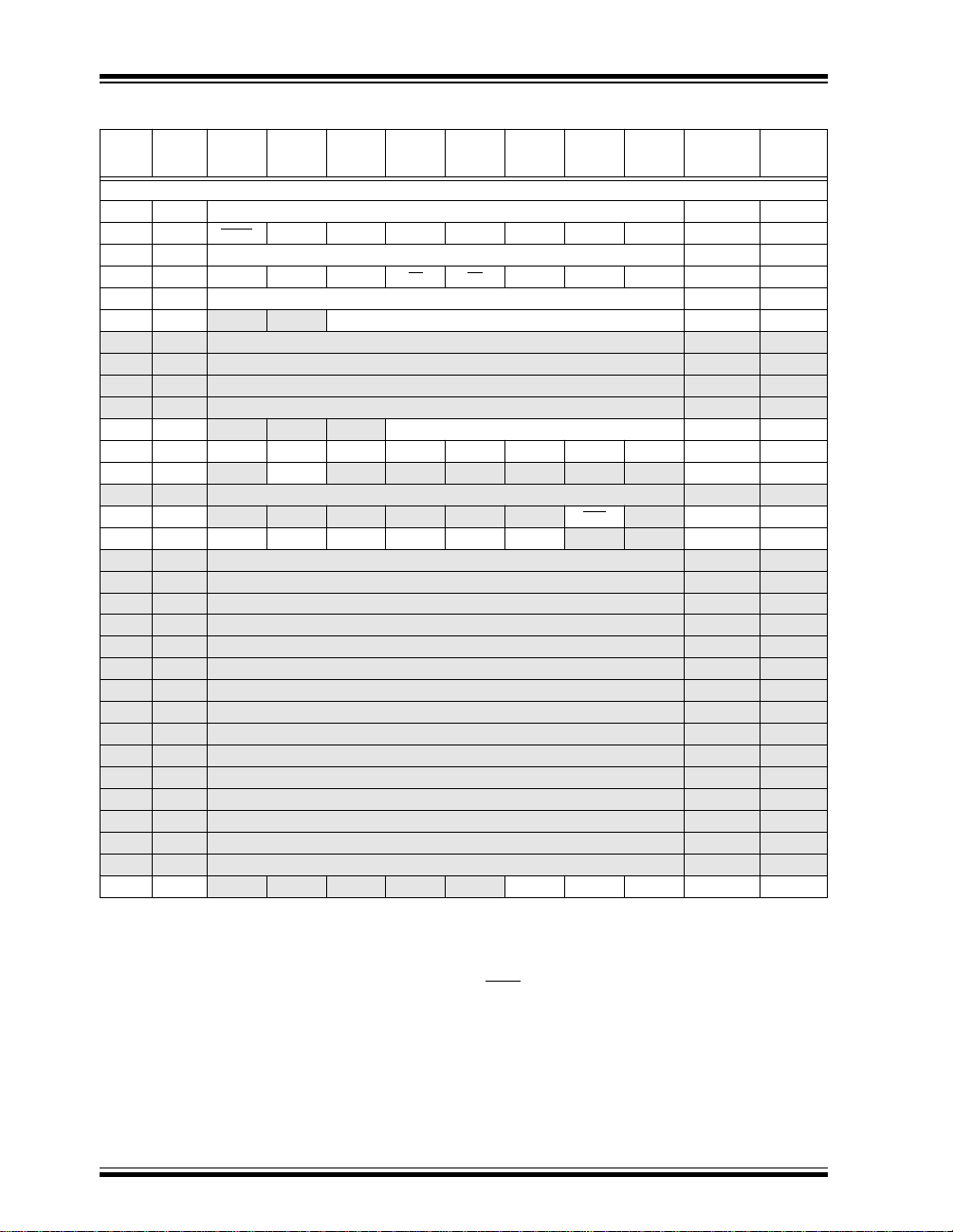
PIC12CE67X
TABLE 4-1: PIC12CE67X SPECIAL FUNCTION REGISTER SUMMARY (CONT.)
Address Name Bit 7 Bit 6 Bit 5 Bit 4 Bit 3 Bit 2 Bit 1 Bit 0
Bank 1
(1)
80h
INDF Addressing this location uses contents of FSR to address data memory (not a physical register) 0000 0000 0000 0000
81h OPTION GPPU INTEDG T0CS T0SE PSA PS2 PS1 PS0 1111 1111 1111 1111
(1)
82h
PCL Program Counter's (PC) Least Significant Byte 0000 0000 0000 0000
(1)
83h
STATUS IRP
(1)
84h
FSR Indirect data memory address pointer xxxx xxxx uuuu uuuu
85h TRIS — — GPIO Data Direction Register 0011 1111 0011 1111
86h — Unimplemented — —
87h — Unimplemented — —
88h — Unimplemented — —
89h — Unimplemented — —
(1,2)
8Ah
PCLATH — — — Write Buffer for the upper 5 bits of the PC ---0 0000 ---0 0000
(1)
8Bh
INTCON GIE PEIE T0IE INTE GPIE T0IF INTF GPIF 0000 000x 0000 000x
8Ch PIE1 — ADIE — — — — — — -0-- ---- -0-- ----
8Dh — Unimplemented — —
8Eh PCON — — — — — — POR — ---- --0- ---- --u-
8Fh OSCCAL CAL5 CAL4 CAL3 CAL2 CAL1 CAL0 — — 1000 00-- uuuu uu--
90h — Unimplemented — —
91h — Unimplemented — —
92h — Unimplemented — —
93h — Unimplemented — —
94h — Unimplemented — —
95h — Unimplemented — —
96h — Unimplemented — —
97h — Unimplemented — —
98h — Unimplemented — —
99h — Unimplemented — —
9Ah — Unimplemented — —
9Bh — Unimplemented — —
9Ch — Unimplemented — —
9Dh — Unimplemented — —
9Eh — Unimplemented — —
9Fh ADCON1 — — — — — PCFG2 PCFG1 PCFG0 ---- -000 ---- -000
(4)
RP1
(4)
RP0 TO PD Z DC C 0001 1xxx 000q quuu
Value on
Power-on
Reset
Legend: x = unknown, u = unchanged, q = value depends on condition, - = unimplemented read as '0', r = reserved.
Shaded locations are unimplemented, read as ‘0’.
Note 1: These registers can be addressed from either bank.
2: The upper byte of the program counter is not directly accessible. PCLATH is a holding register for the PC<12:8> whose
contents are transferred to the upper byte of the program counter.
3: Other (non power-up) resets include external reset through MCLR and Watchdog Timer Reset.
4: The IRP and RP1 bits are reserved on the PIC12CE67X, always maintain these bits clear.
Value on
all other
Resets
(3)
DS40181A-page 14 Preliminary 1998 Microchip Technology Inc.

PIC12CE67X
4.2.2.1 STATUS REGISTER
The STATUS register, shown in Figure 4-3, contains
the arithmetic status of the ALU, the RESET status and
the bank select bits for data memory.
The STATUS register can be the destination for any
instruction, as with any other register. If the STATUS
register is the destination for an instruction that affects
the Z, DC or C bits, then the write to these three bits is
disabled. These bits are set or cleared according to the
device logic. Further more, the T
writable. Therefore, the result of an instruction with the
STATUS register as destination may be different than
intended.
For example, CLRF STATUS will clear the upper-three
bits and set the Z bit. This lea v es the STATUS register
as 000u u1uu (where u = unchanged).
O and PD bits are not
It is recommended, therefore, that only BCF, BSF,
SWAPF and MOVWF instructions are used to alter the
STATUS register because these instructions do not
affect the Z, C or DC bits from the STATUS register. For
other instructions, not affecting any status bits, see the
"Instruction Set Summary."
Note 1: Bits IRP and RP1 (STATUS<7:6>) are not
used by the PIC12CE67X and should be
maintained clear. Use of these bits as
general purpose R/W bits is NOT recommended, since this may affect upward
compatibility with future products.
Note 2: The C and DC bits operate as a borro
and digit borrow bit, respectively, in subtraction. See the SUBLW and SUBWF
instructions for examples.
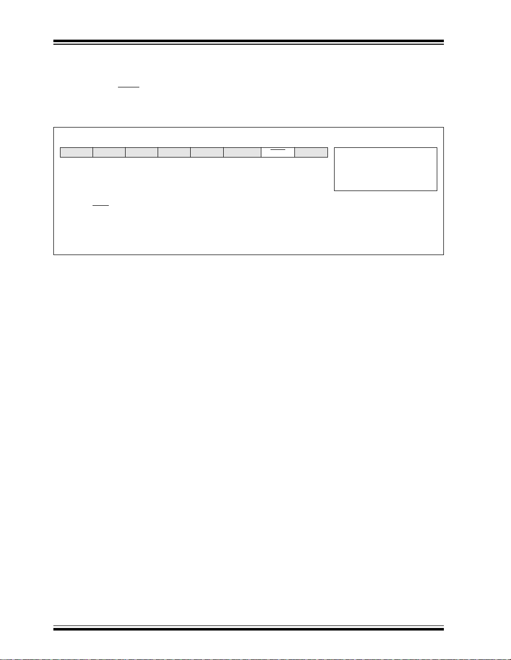
FIGURE 4-3: STATUS REGISTER (ADDRESS 03h, 83h)
Reserved Reserved R/W-0 R-1 R-1 R/W-x R/W-x R/W-x
IRP RP1 RP0 TO PD Z DC C R = Readable bit
bit7 bit0
bit 7: IRP: Register Bank Select bit (used for indirect addressing)
1 = Bank 2, 3 (100h - 1FFh)
0 = Bank 0, 1 (00h - FFh)
The IRP bit is reserved, always maintain this bit clear.
bit 6-5: RP1:RP0: Register Bank Select bits (used for direct addressing)
11 = Bank 3 (180h - 1FFh)
10 = Bank 2 (100h - 17Fh)
01 = Bank 1 (80h - FFh)
00 = Bank 0 (00h - 7Fh)
Each bank is 128 bytes. The RP1 bit is reserved, always maintain this bit clear.
bit 4: T
bit 3: PD
bit 2: Z: Zero bit
bit 1: DC: Digit carry/borro
bit 0: C: Carry/borro
O: Time-out bit
1 = After power-up, CLRWDT instruction, or SLEEP instruction
0 = A WDT time-out occurred
: Power-down bit
1 = After power-up or by the CLRWDT instruction
0 = By execution of the SLEEP instruction
1 = The result of an arithmetic or logic operation is zero
0 = The result of an arithmetic or logic operation is not zero
1 = A carry-out from the 4th low order bit of the result occurred
0 = No carry-out from the 4th low order bit of the result
1 = A carry-out from the most significant bit of the result occurred
0 = No carry-out from the most significant bit of the result occurred
Note: For borro
second operand. For rotate (RRF, RLF) instructions, this bit is loaded with either the high or low order bit of
the source register.
w bit (ADDWF, ADDLW,SUBLW,SUBWF instructions)(for borrow the polarity is reversed)
w bit (ADDWF, ADDLW,SUBLW,SUBWF instructions)
w the polarity is reversed. A subtraction is executed by adding the two’s complement of the
W = Writable bit
U = Unimplemented bit,
read as ‘0’
- n = Value at POR reset
w
1998 Microchip Technology Inc. Preliminary DS40181A-page 15

PIC12CE67X
4.2.2.2 OPTION REGISTER
The OPTION register is a readable and writable regis-
ter which contains various control bits to configure the
TMR0/WDT prescaler, the External INT Interrupt,
Note: To achieve a 1:1 prescaler assignment for
the TMR0 register, assign the prescaler to
the Watchdog Timer by setting bit PSA
(OPTION<3>).
TMR0, and the weak pull-ups on GPIO.
FIGURE 4-4: OPTION REGISTER (ADDRESS 81h)
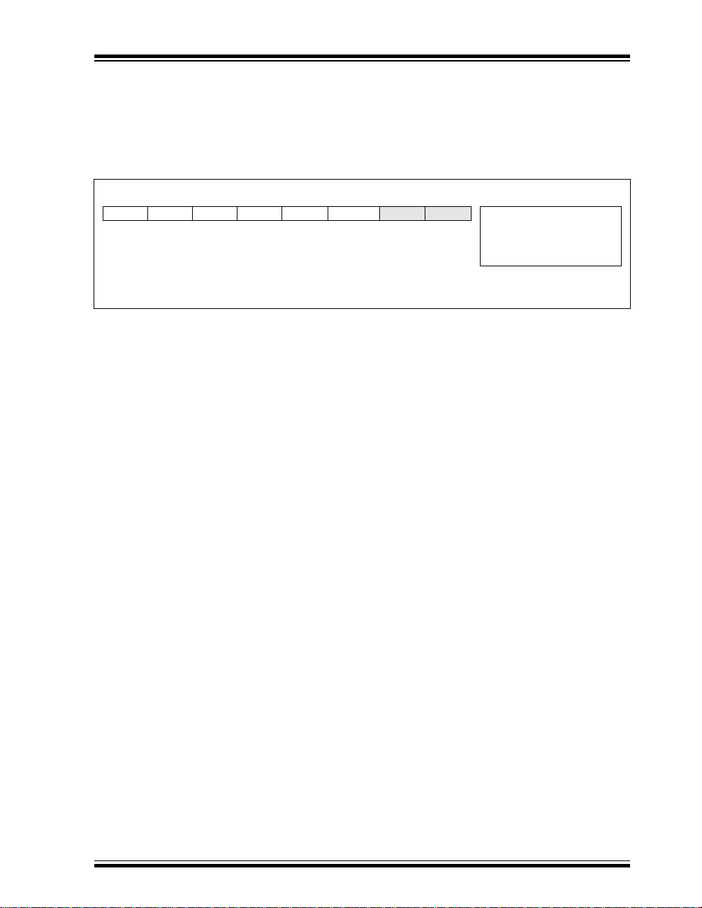
R/W-1 R/W-1 R/W-1 R/W-1 R/W-1 R/W-1 R/W-1 R/W-1
INTEDG T0CS T0SE PSA PS2 PS1 PS0 R = Readable bit
GPPU
bit7 bit0
bit 7: GPPU: Weak pullup enable
1 = Weak pullups disabled
0 = Weak pullups enabled (GP0, GP1, GP3)
bit 6: INTEDG: Interrupt edge
1 = Interrupt on rising edge of GP2/INT pin
0 = Interrupt on falling edge of GP2/INT pin
bit 5: T0CS: TMR0 Clock Source Select bit
1 = Transition on GP2/T0CKI/AN2 pin
0 = Internal instruction cycle clock (CLKOUT)
bit 4: T0SE: TMR0 Source Edge Select bit
1 = Increment on high-to-low transition on GP2/T0CKI/AN2 pin
0 = Increment on low-to-high transition on GP2/T0CKI/AN2 pin
bit 3: PSA: Prescaler Assignment bit
1 = Prescaler is assigned to the WDT
0 = Prescaler is assigned to the Timer0 module
bit 2-0: PS2:PS0: Prescaler Rate Select bits
Bit Value TMR0 Rate WDT Rate
000
001
010
011
100
101
110
111
1 : 2
1 : 4
1 : 8
1 : 16
1 : 32
1 : 64
1 : 128
1 : 256
1 : 1
1 : 2
1 : 4
1 : 8
1 : 16
1 : 32
1 : 64
1 : 128
W = Writable bit
U = Unimplemented bit,
read as ‘0’
- n = Value at POR reset
DS40181A-page 16 Preliminary 1998 Microchip Technology Inc.

PIC12CE67X
4.2.2.3 INTCON REGISTER
The INTCON Register is a readable and writable regis-
ter which contains various enable and flag bits for the
TMR0 register overflow, GPIO Port change and External GP2/INT Pin interrupts.
Note: Interrupt flag bits get set when an interrupt
condition occurs regardless of the state of
its corresponding enable bit or the global
enable bit, GIE (INTCON<7>).
FIGURE 4-5: INTCON REGISTER (ADDRESS 0Bh, 8Bh)
R/W-0 R/W-0 R/W-0 R/W-0 R/W-0 R/W-0 R/W-0 R/W-x
GIE PEIE T0IE INTE GPIE T0IF INTF GPIF R = Readable bit
bit7 bit0
bit 7: GIE: Global Interrupt Enable bit
1 = Enables all un-masked interrupts
0 = Disables all interrupts
bit 6: PEIE: Peripheral Interrupt Enable bit
1 = Enables all un-masked peripheral interrupts
0 = Disables all peripheral interrupts
bit 5: T0IE: TMR0 Overflow Interrupt Enable bit
1 = Enables the TMR0 interrupt
0 = Disables the TMR0 interrupt
bit 4: INTE: INT External Interrupt Enable bit
1 = Enables the external interrupt on GP2/INT pin
0 = Disables the external interrupt on GP2/INT pin
bit 3: GPIE: GPIO Interrupt on Change Enable bit
1 = Enables the GPIO Interrupt on Change
0 = Disables the GPIO Interrupt on Change
bit 2: T0IF: TMR0 Overflow Interrupt Flag bit
1 = TMR0 register has overflowed (must be cleared in software)
0 = TMR0 register did not overflow
bit 1: INTF: INT External Interrupt Flag bit
1 = The external interrupt on GP2/INT pin occurred (must be cleared in software)
0 = The external interrupt on GP2/INT pin did not occur
bit 0: GPIF: GPIO Interrupt on Change Flag bit
1 = GP0, GP1, or GP3 pins changed state (must be cleared in software)
0 = Neither GP0, GP1, nor GP3 pins have changed state
W = Writable bit
U = Unimplemented bit,
- n = Value at POR reset
read as ‘0’
1998 Microchip Technology Inc. Preliminary DS40181A-page 17

PIC12CE67X
4.2.2.4 PIE1 REGISTER
This register contains the individual enable bits for the
Peripheral interrupts.
Note: Bit PEIE (INTCON<6>) must be set to
enable any peripheral interrupt.
FIGURE 4-6: PIE1 REGISTER (ADDRESS 8Ch)
U-0 R/W-0 U-0 U-0 U-0 U-0 U-0 U-0
— ADIE — — — — — — R = Readable bit
bit7 bit0
bit 7: Unimplemented: Read as '0'
bit 6: ADIE: A/D Converter Interrupt Enable bit
1 = Enables the A/D interrupt
0 = Disables the A/D interrupt
bit 5-0: Unimplemented: Read as '0'
W = Writable bit
U = Unimplemented bit,
- n = Value at POR reset
read as ‘0’
DS40181A-page 18 Preliminary 1998 Microchip Technology Inc.

PIC12CE67X
4.2.2.5 PIR1 REGISTER
This register contains the individual flag bits for the
Peripheral interrupts.
Note: Interrupt flag bits get set when an interrupt
condition occurs regardless of the state of
its corresponding enable bit or the global
enable bit, GIE (INTCON<7>). User software should ensure the appropriate interrupt flag bits are clear prior to enabling an
interrupt.
FIGURE 4-7: PIR1 REGISTER (ADDRESS 0Ch)
U-0 R/W-0 U-0 U-0 U-0 U-0 U-0 U-0
— ADIF — — — — — — R = Readable bit
bit7 bit0
bit 7: Unimplemented: Read as '0'
bit 6: ADIF: A/D Converter Interrupt Flag bit
1 = An A/D conversion completed
0 = The A/D conversion is not complete
bit 5-0: Unimplemented: Read as '0'
W = Writable bit
U = Unimplemented bit,
- n = Value at POR reset
read as ‘0’
1998 Microchip Technology Inc. Preliminary DS40181A-page 19
PIC12CE67X
4.2.2.6 PCON REGISTER
The Power Control (PCON) register contains a flag bit
to allow differentiation between a Power-on Reset
(POR), an external MCLR
FIGURE 4-8: PCON REGISTER (ADDRESS 8Eh)
U-0 U-0 U-0 U-0 U-0 U-0 R/W-0 U-0
— — — — — — POR — R = Readable bit
bit7 bit0
bit 7-2: Unimplemented: Read as '0'
bit 1: POR
bit 0: Unimplemented: Read as '0'
: Power-on Reset Status bit
1 = No Power-on Reset occurred
0 = A Power-on Reset occurred (must be set in software after a Power-on Reset occurs)
Reset, and WDT Reset.
W = Writable bit
U = Unimplemented bit,
- n = Value at POR reset
read as ‘0’
DS40181A-page 20 Preliminary 1998 Microchip Technology Inc.
PIC12CE67X
4.2.2.7 OSCCAL REGISTER
The Oscillator Calibration (OSCCAL) register is used to
calibrate the internal 4 MHz oscillator. It contains six
bits for calibration. Increasing the cal value increases
the frequency.
FIGURE 4-9: OSCCAL REGISTER (ADDRESS 8Fh)
R/W-1 R/W-0 R/W-0 R/W-0 R/W-0 R/W-0 U-0 U-0
CAL5 CAL4 CAL3 CAL2 CAL1 CAL0 — — R = Readable bit
bit7 bit0
bit 7-2: CAL<5:0>: Calibration
W = Writable bit
U = Unimplemented bit,
- n = Value at POR reset
read as ‘0’
1998 Microchip Technology Inc. Preliminary DS40181A-page 21
PIC12CE67X
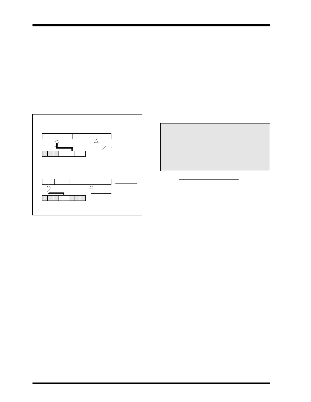
4.3 PCL and PCLATH
The program counter (PC) is 13-bits wide. The low b yte
comes from the PCL register, which is a readable and
writable register. The high byte (PC<12:8>) is not
directly readable or writable and comes from PCLATH.
On any reset, the PC is cleared. Figure 4-10 shows the
two situations for the loading of the PC. The upper
example in the figure shows how the PC is loaded on a
write to PCL (PCLA TH<4:0> → PCH). The lower e xample in the figure shows how the PC is loaded during a
CALL or GOTO instruction (PCLATH<4:3> → PCH).
FIGURE 4-10: LOADING OF PC IN
DIFFERENT SITUATIONS
PCH PCL
12 8 7 0
PC
PCLA TH<4:0>
5
PCLA TH
PCH PCL
12 11 10 0
PC
2
8 7
PCLATH<4:3>
PCLATH
11
4.3.1 COMPUTED GOTO A computed GOTO is accomplished by adding an off-
set to the program counter (ADDWF PCL). When doing a
table read using a computed GOTO method, care
should be exercised if the table location crosses a PCL
memory boundary (each 256 byte block). Refer to the
application note
“Implementing a Table Read"
8
Instr
uction with
PCL as
Destination
ALU result
GOTO, CALL
Opcode <10:0>
(AN556).
4.3.2 STACK The PIC12CE67X family has an 8 level deep x 13-bit
wide hardware stack. The stack space is not part of
either program or data space and the stack pointer is
not readable or writable. The PC is PUSHed onto the
stack when a CALL instruction is executed or an interrupt causes a branch. The stack is POPed in the event
of a RETURN, RETLW or a RETFIE instruction execution.
PCLA TH is not affected by a PUSH or POP operation.
The stack operates as a circular buffer . This means that
after the stack has been PUSHed eight times, the ninth
push overwrites the value that was stored from the first
push. The tenth push overwrites the second push (and
so on).
Note 1: There are no status bits to indicate stack
overflow or stack underflow conditions.
Note 2: There are no instructions/mnemonics
called PUSH or POP. These are actions
that occur from the execution of the CALL,
RETURN, RETLW, and RETFIE instructions, or the vectoring to an interrupt
address.
4.4 Program Memory Paging
The PIC12CE67X ignores both paging bits
PCLATH<4:3>, which are used to access program
memory when more than one page is available. The
use of PCLATH<4:3> as general purpose read/write
bits for the PIC12CE67X is not recommended since
this may affect upward compatibility with future products.
DS40181A-page 22 Preliminary 1998 Microchip Technology Inc.
PIC12CE67X
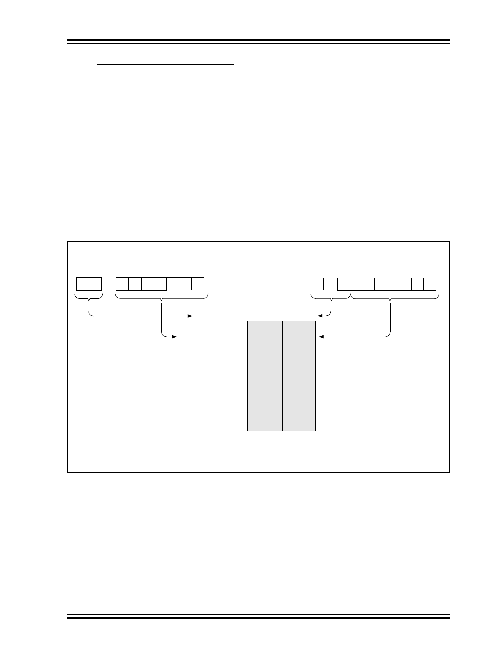
4.5 Indirect Addressing, INDF and FSR
Registers
The INDF register is not a physical register. Addressing
the INDF register will cause indirect addressing.
Indirect addressing is possible by using the INDF register. Any instruction using the INDF register actually
accesses the register pointed to by the File Select Register, FSR. Reading the INDF register itself indirectly
(FSR = '0') will read 00h. Writing to the INDF register
indirectly results in a no-operation (although status bits
may be affected). An effective 9-bit address is obtained
by concatenating the 8-bit FSR register and the IRP bit
(STA TUS<7>), as shown in Figure 4-11. However, IRP
is not used in the PIC12CE67X.
A simple program to clear RAM locations 20h-2Fh
using indirect addressing is shown in Example 4-1.
FIGURE 4-11: DIRECT/INDIRECT ADDRESSING
(1)
RP1 RP0 6
bank select location select
from opcode
00h
0
00 01 10 11
EXAMPLE 4-1: INDIRECT ADDRESSING
movlw 0x20 ;initialize pointer
movwf FSR ;to RAM
NEXT clrf INDF ;clear INDF register
incf FSR,F ;inc pointer
btfss FSR,4 ;all done?
goto NEXT ;no clear next
CONTINUE
: ;yes continue
Indirect AddressingDirect Addressing
(1)
IRP
bank select
00h
7
FSR register
location select
0
Data
Memory
7Fh
not used
7Fh
Bank 0 Bank 1 Bank 2 Bank 3
For register file map detail see Figure 4-2.
Note 1: The RP1 and IRP bits are reserved, always maintain these bits clear.
1998 Microchip Technology Inc. Preliminary DS40181A-page 23

PIC12CE67X
NOTES:
DS40181A-page 24 Preliminary 1998 Microchip Technology Inc.
PIC12CE67X
5.0 I/O PORT
As with any other register, the I/O register can be
written and read under program control. However,
read instructions (e.g., MOVF GPIO,W) always read the
I/O pins independent of the pin’s input/output modes.
On RESET, all I/O ports are defined as input (inputs
are at hi-impedance) since the I/O control registers are
all set.
5.1 GPIO
GPIO is an 8-bit I/O register. Only the low order 6 bits
are used (GP5:GP0). Bits 6 and 7 (SDA and SCL) are
used by the EEPROM peripheral. Refer to Section 6.0
and Appendix A for use of SDA and SCL. Please note
that GP3 is an input only pin. The configuration word
can set several I/O’s to alternate functions. When
acting as alternate functions the pins will read as ‘0’
during port read. Pins GP0, GP1, and GP3 can be
configured with weak pull-ups and also with interrupt
on change. The interrupt on change and weak pull-up
functions are not pin selectable. If pin 4 is configured
as MCLR
change for this pin is not set and GP3 will read as '0'.
Interrupt on change is enabled by setting INTCON<3>.
Note that external oscillator use overrides the GPIO
functions on GP4 and GP5.
5.2 TRIS Register
This register controls the data direction for GPIO. A '1'
from a TRIS register bit puts the corresponding output
driver in a hi-impedance mode. A '0' puts the contents
of the output data latch on the selected pins, enabling
the output buffer. The exceptions are GP3 which is
input only and its TRIS bit will always read as '1'.
Upon reset, the TRIS register is all '1's, making all pins
inputs.
, the weak pull-up is always on. Interrupt on
Note: A read of the ports reads the pins, not the
output data latches. That is, if an output
driver on a pin is enabled and driven high,
but the external system is holding it low, a
read of the port will indicate that the pin is
low.
5.3 I/O Interfacing
The equivalent circuit for an I/O port pin is shown in
Figure 5-2. All port pins, except GP3 which is input
only, may be used for both input and output
operations. For input operations these ports are nonlatching. Any input must be present until read by an
input instruction (e.g., MOVF GPIO,W). The outputs are
latched and remain unchanged until the output latch is
rewritten. To use a port pin as output, the
corresponding direction control bit in TRIS must be
cleared (= 0). For use as an input, the corresponding
TRIS bit must be set. Any I/O pin (except GP3) can be
programmed individually as input or output.
Note: On a Power-on Reset, GP0, GP1, GP2,
GP4 are configured as analog inputs and
read as '0'.
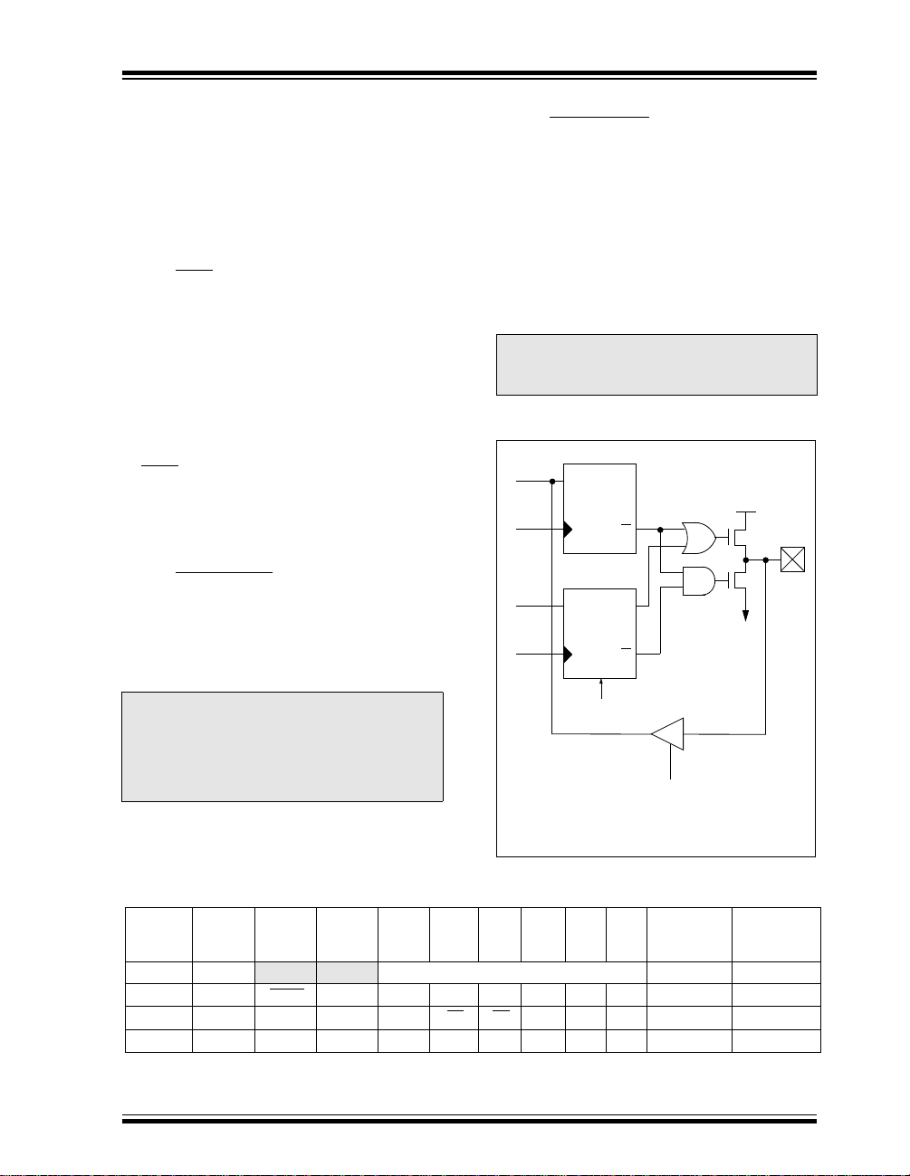
FIGURE 5-1: EQUIVALENT CIRCUIT
FOR A SINGLE I/O PIN
Data
Bus
WR
Port
W
Reg
TRIS ‘f’
Note 1: I/O pins have protection diodes to VDD and VSS.
GP3 is input only with no data latch and no
output drivers.
Data
Latch
CK
TRIS
Latch
CK
Reset
QD
VDD
Q
QD
Q
RD Port
P
N
VSS
I/O
pin
(1)
TABLE 5-1: SUMMARY OF PORT REGISTERS
Value on
Address Name Bit 7 Bit 6 Bit 5 Bit 4 Bit 3 Bit 2 Bit 1 Bit 0
85h TRIS
81h OPTION GPPU INTEDG T0CS T0SE PSA PS2 PS1 PS0 1111 1111 1111 1111
03h STATUS
05h GPIO SCL SDA GP5 GP4 GP3 GP2 GP1 GP0 11xx xxxx 11uu uuuu
Legend: Shaded cells not used by Port Registers, read as ‘0’, — = unimplemented, read as '0', x = unknown, u = unchanged,
q = see tables in Section 9.4 for possible values.
Note 1: The IRP and RP1 bits are reserved on the PIC12CE67X, always maintain these bits clear.
1998 Microchip Technology Inc. Preliminary DS40181A-page 25
— — GPIO Data Direction Register --11 1111 --11 1111
IRP
(1)
RP1
(1)
RP0 TO PD Z DC C 0001 1xxx 000q quuu
Power-on
Reset
Value on
all other
Resets
PIC12CE67X
5.4 I/O Programming Considerations
5.4.1 BI-DIRECTIONAL I/O PORTS Any instruction which writes, operates internally as a
read followed by a write operation. The BCF and BSF
instructions, for example, read the register into the
CPU, ex ecute the bit operation and write the result back
to the register. Caution must be used when these
instructions are applied to a port with both inputs and
outputs defined. For example, a BSF operation on bit5
of GPIO will cause all eight bits of GPIO to be read into
the CPU. Then the BSF operation takes place on bit5
and GPIO is written to the output latches. If another bit
of GPIO is used as a bi-directional I/O pin (e.g., bit0)
and it is defined as an input at this time, the input signal
present on the pin itself would be read into the CPU
and rewritten to the data latch of this particular pin,
overwriting the previous content. As long as the pin
stays in the input mode, no problem occurs. However,
if bit0 is switched to an output, the content of the data
latch may now be unknown.
Reading the port register, reads the values of the port
pins. Writing to the port register writes the value to the
port latch. When using read-modify-write instructions
(ex. BCF, BSF , etc.) on a port, the value of the port pins
is read, the desired operation is done to this value, and
this value is then written to the port latch.
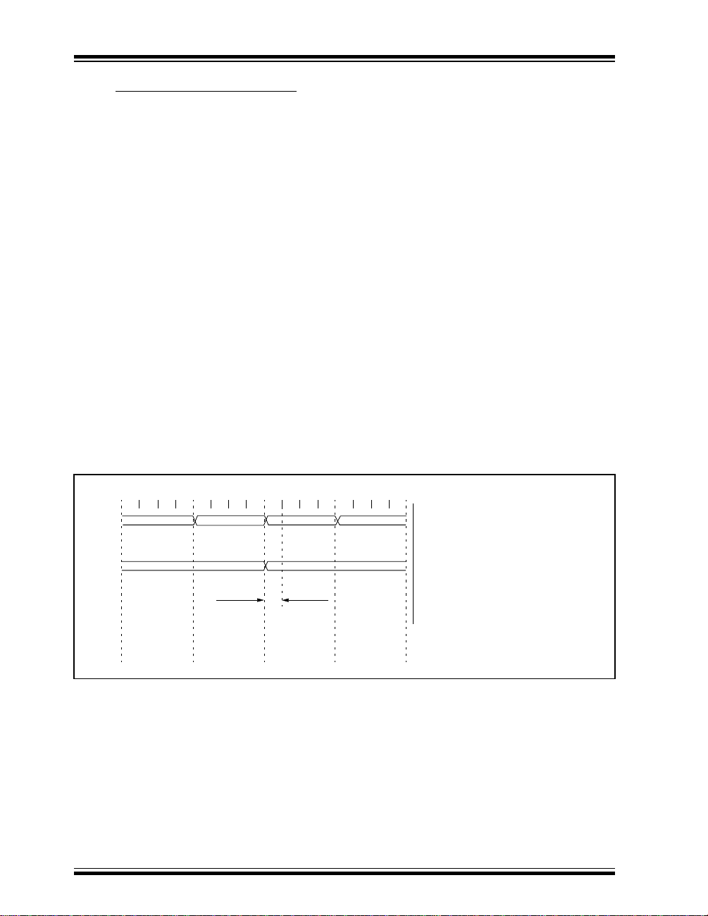
FIGURE 5-2: SUCCESSIVE I/O OPERATION
Example 5-1 shows the effect of two sequential read-
modify-write instructions on an I/O port.
EXAMPLE 5-1: READ-MODIFY-WRITE
INSTRUCTIONS ON AN
I/O PORT
;Initial GPIO Settings
; GPIO<5:3> Inputs
; GPIO<2:0> Outputs
;
; GPIO latch GPIO pins
; ---------- --------- BCF GPIO, 5 ;--01 -ppp --11 pppp
BCF GPIO, 4 ;--10 -ppp --11 pppp
MOVLW 007h ;
TRIS GPIO ;--10 -ppp --11 pppp
;
;Note that the user may have expected the pin
;values to be --00 pppp. The 2nd BCF caused
;GP5 to be latched as the pin value (High).
A pin actively outputting a Low or High should not be
driven from external devices at the same time in order
to change the level on this pin (“wired-or”, “wired-and”).
The resulting high output currents may damage the
chip.
Q4
Q3
Q1 Q2
Instruction
fetched
GP5:GP0
Instruction
executed
DS40181A-page 26 Preliminary 1998 Microchip Technology Inc.
PC PC + 1 PC + 2
MOVWF GPIO
Q1 Q2
MOVF GPIO,W
MOVWF GPIO
Q3
Port pin
written here
(Write to
GPIO)
Q4
Q1 Q2
MOVF GPIO,W
Q3
NOP
Port pin
sampled here
(Read
GPIO)
Q4
Q1 Q2
Q3
PC + 3
NOP
NOP
Q4
This example shows a write to GPIO followed
by a read from GPIO.
Data setup time = (0.25 TCY – TPD)
where: TCY = instruction cycle.
TPD = propagation delay
Therefore, at higher clock frequencies, a
write followed by a read may be problematic.

PIC12CE67X
6.0 EEPROM PERIPHERAL
OPERATION
The PIC12CE673 and PIC12CE674 each have 16
bytes of EEPROM data memory. The EEPROM memory has an endurance of 1,000,000 erase/write cycles
and a data retention of greater than 40 years. The
EEPROM data memory supports a bi-directional 2-wire
bus and data transmission protocol. These two-wires
are serial data (SDA) and serial clock (SCL), that are
mapped to bit6 and bit7, respectively, of the GPIO register (SFR 06h). Unlike the GP0-GP5 that are connected to the I/O pins, SDA and SCL are only
connected to the internal EEPROM peripheral. For
most applications, all that is required is calls to the following functions:
; Byte_Write: Byte write routine
; Inputs: EEPROM Address EEADDR
; EEPROM Data EEDATA
; Outputs: Return 01 in W if OK, else
return 00 in W
;
; Read_Current: Read EEPROM at address
currently held by EE device.
; Inputs: NONE
; Outputs: EEPROM Data EEDATA
; Return 01 in W if OK, else
return 00 in W
;
; Read_Random: Read EEPROM byte at supplied
address
; Inputs: EEPROM Address EEADDR
; Outputs: EEPROM Data EEDATA
; Return 01 in W if OK,
else return 00 in W
The code for these functions is not yet determined, but
will be available on our web site (www.microchip.com)
when it is completed. The code will be accessed by
either including the source code FLASH67X.INC or by
linking FLASH67X.ASM.
6.0.1 SERIAL DATA
SDA is a bi-directional pin used to transfer addresses
and data into and data out of the device.
For normal data transfer SDA is allo wed to change only
during SCL low. Changes during SCL high are
reserved for indicating the START and STOP conditions.
6.0.2 SERIAL CLOCK
This SCL input is used to synchronize the data transf er
from and to the EEPROM.
6.1 BUS CHARACTERISTICS
The following bus protocol is to be used with the
EEPROM data memory. In this section, the term “processor” is used to denote the portion of the
PIC12CE67X that interfaces to the EEPROM via software.
• Data transfer may be initiated only when the bus
is not busy.
During data transfer, the data line must remain stable
whenever the clock line is HIGH. Changes in the data
line while the clock line is HIGH will be interpreted as a
START or STOP condition.
Accordingly, the following bus conditions have been
defined (Figure 6-1).
6.1.1 BUS NOT BUSY (A)
Both data and clock lines remain HIGH.
6.1.2 START DATA TRANSFER (B)
A HIGH to LOW transition of the SDA line while the
clock (SCL) is HIGH determines a ST AR T condition. All
commands must be preceded by a START condition.
6.1.3 STOP DATA TRANSFER (C)
A LOW to HIGH transition of the SDA line while the
clock (SCL) is HIGH determines a STOP condition. All
operations must be ended with a STOP condition.
6.1.4 DATA VALID (D)
The state of the data line represents valid data when,
after a START condition, the data line is stable for the
duration of the HIGH period of the clock signal.
The data on the line must be changed during the LOW
period of the clock signal. There is one bit of data per
clock pulse.
Each data transfer is initiated with a START condition
and terminated with a STOP condition. The number of
the data bytes transferred between the START and
STOP conditions is determined by the processor
device and is theoretically unlimited.
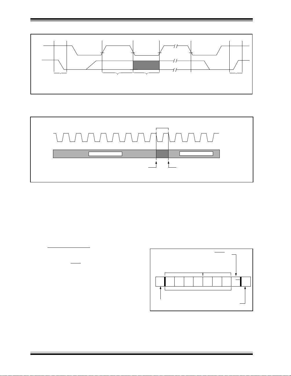
6.1.5 ACKNOWLEDGE
The EEPROM, when addressed, will generate an
acknowledge after the reception of each byte. The processor must generate an extra clock pulse which is
associated with this acknowledge bit.
Note: Acknowledge bits are not generated if an
internal programming cycle is in progress.
The device that acknowledges has to pull down the
SDA line during the acknowledge clock pulse in such a
way that the SDA line is stable LOW during the HIGH
period of the acknowledge related clock pulse. Of
course, setup and hold times must be taken into
account. The processor must signal an end of data to
the EEPROM by not generating an acknowledge bit on
the last byte that has been clocked out of the EEPROM.
In this case, the EEPROM must leave the data line
HIGH to enable the processor to generate the STOP
condition (Figure 6-2).
1998 Microchip Technology Inc. Preliminary DS40181A-page 27
PIC12CE67X
FIGURE 6-1: DATA TRANSFER SEQUENCE ON THE SERIAL BUS
SCL
SDA
(A)
START
CONDITION
(C)
ADDRESS OR
ACKNOWLEDGE
VALID
(B)
FIGURE 6-2: ACKNOWLEDGE TIMING
SCL
SDA
Data from transmitter
Transmitter must release the SDA line at this point
allowing the Receiver to pull the SDA line low to
acknowledge the previous eight bits of data.
DATA
ALLOWED
TO CHANGE
Acknowledge
(D)
Bit
987654321 1 2 3
Data from transmitter
Receiver must release the SDA line at this point
so the Transmitter can continue sending data.
STOP
CONDITION
(A)(C)
6.2 Device Addressing
After generating a START condition, the processor
FIGURE 6-3: CONTROL BYTE FORMAT
Read/Wr
ite Bit
transmits a control byte consisting of a EEPROM
address and a Read/Wr
ite bit that indicates what type
of operation is to be performed. The EEPROM address
Device Select
Bits
Don’t Care
Bits
consists of a 4-bit device code (1010) followed b y three
don't care bits.
1 0 1 0 X X XS ACKR/W
The last bit of the control byte determines the operation
to be performed. When set to a one a read operation is
selected, and when set to a zero a write operation is
selected. (Figure 6-3). The bus is monitored for its cor-
Start Bit
EEPROM Address
Acknowledge Bit
responding EEPROM address all the time. It generates
an acknowledge bit if the EEPROM address was true
and it is not in a programming mode.
DS40181A-page 28 Preliminary 1998 Microchip Technology Inc.
PIC12CE67X
6.3 WRITE OPERATIONS
6.3.1 BYTE WRITE Following the start signal from the processor, the
device code (4 bits), the don't care bits (3 bits), and the
R/W
bit (which is a logic low) are placed onto the bus
by the processor. This indicates to the addressed
EEPROM that a byte with a word address will follow
after it has generated an acknowledge bit during the
ninth clock cycle. Therefore, the next byte transmitted
by the processor is the word address and will be written
into the address pointer. Only the lower four address
bits are used by the device, and the upper four bits are
don’t cares. The address byte is acknowledgeable and
the processor will then transmit the data word to be
written into the addressed memory location. The memory acknowledges again and the processor generates
a stop condition. This initiates the internal write cycle,
and during this time will not generate acknowledge signals (Figure 6-5). After a byte write command, the internal address counter will not be incremented and will
point to the same address location that was just written.
If a stop bit is transmitted to the device at any point in
the write command sequence before the entire
sequence is complete, then the command will abort
and no data will be written. If more than 8 data bits are
transmitted before the stop bit is sent, then the device
will clear the previously loaded byte and begin loading
the data buffer again. If more than one data byte is
transmitted to the device and a stop bit is sent before a
full eight data bits have been transmitted, then the write
command will abort and no data will be written. The
EEPROM memory employs a V
circuit which disables the internal erase/write logic if
the V
CC is below minimum VDD.
CC threshold detector
6.4 ACKNOWLEDGE POLLING
Since the EEPROM will not acknowledge during a write
cycle, this can be used to determine when the cycle is
complete (this feature can be used to maximize bus
throughput). Once the stop condition for a write command has been issued from the processor, the device
initiates the internally timed write cycle. ACK polling
can be initiated immediately. This involves the processor sending a start condition followed by the control
byte for a write command (R/W
= 0). If the device is still
busy with the write cycle, then no ACK will be returned.
If no ACK is returned, then the start bit and control byte
must be re-sent. If the cycle is complete, then the
device will return the ACK and the processor can then
proceed with the next read or write command. See
Figure 6-4 for flow diagram.
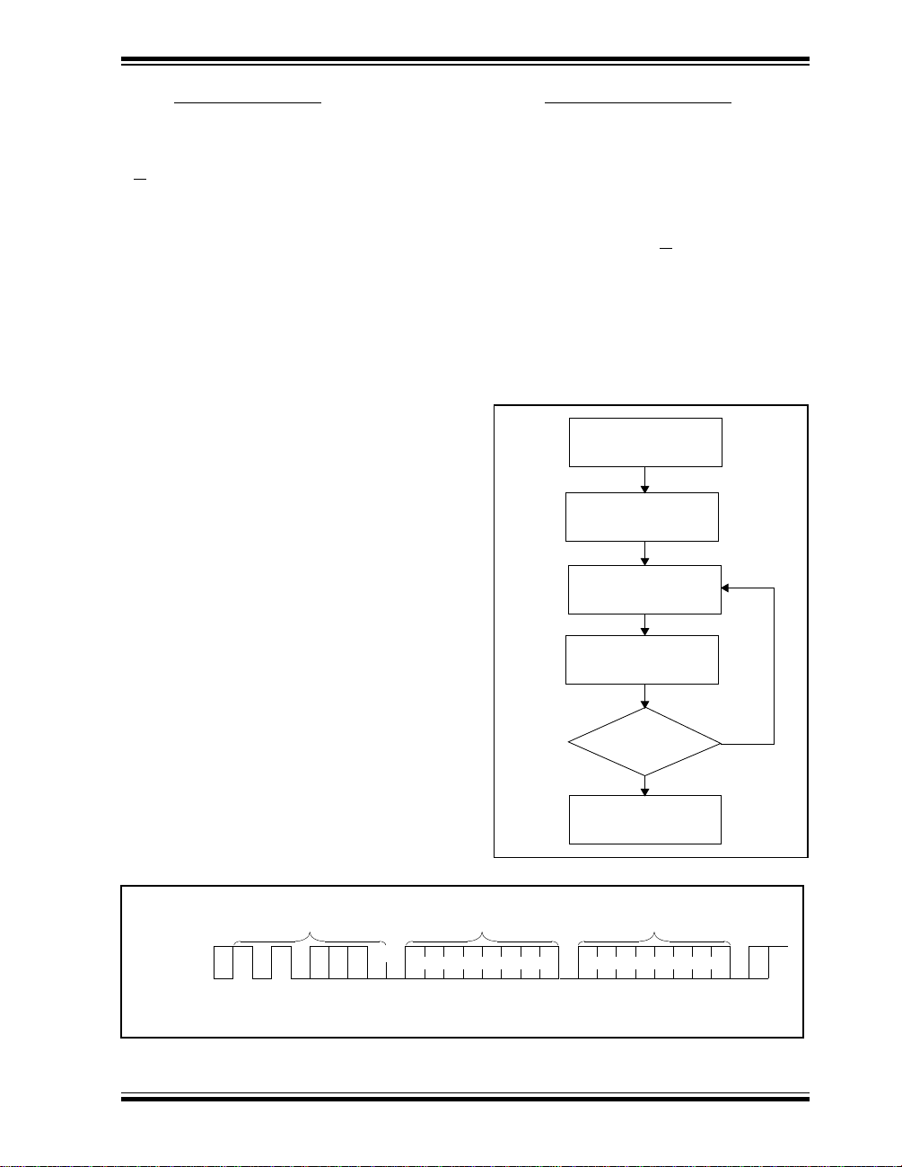
FIGURE 6-4: ACKNOWLEDGE POLLING
FLOW
Send
Write Command
Send Stop
Condition to
Initiate Write Cycle
Send Start
Send Control Byte
with R/W = 0
Did EEPROM
Acknowledge
(ACK = 0)?
NO
YES
Next
Operation
FIGURE 6-5: BYTE WRITE
S
BUS ACTIVITY
PROCESSOR
SDA LINE
BUS ACTIVITY
X = Don’t Care Bit
1998 Microchip Technology Inc. Preliminary DS40181A-page 29
T
A
R
T
S
CONTROL
BYTE
1 0 X1 0 XX X
0
A
C
K
ADDRESS
X X X
WORD
DATA
A
C
K
S
T
O
P
P
A
C
K
PIC12CE67X
6.5 READ OPERATIONS
Read operations are initiated in the same way as write
operations with the exception that the R/W
bit of the
EEPROM address is set to one. There are three basic
types of read operations: current address read, random
read, and sequential read.
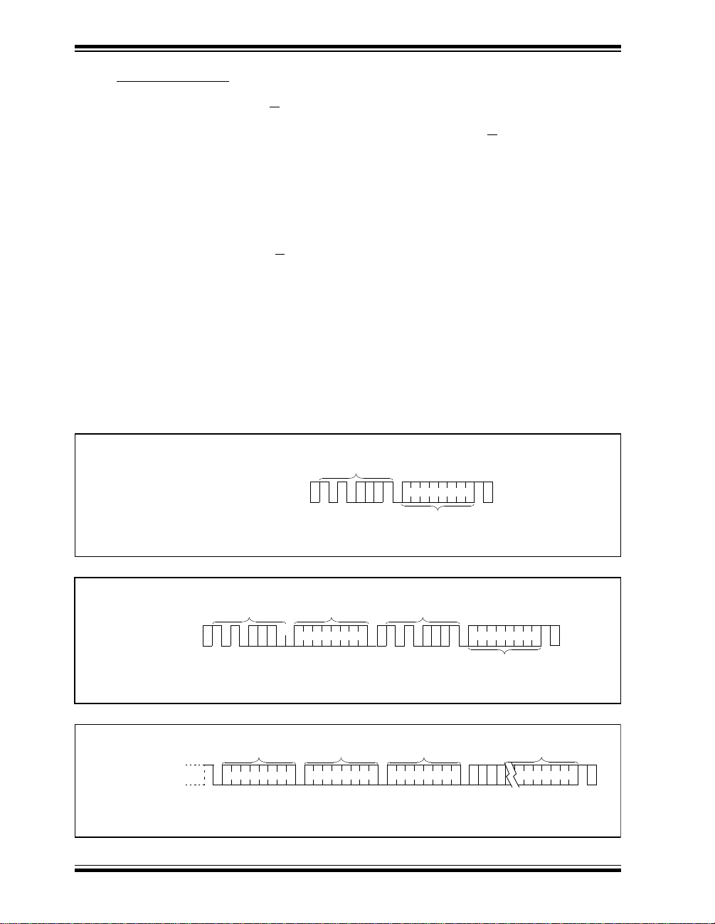
6.5.1 CURRENT ADDRESS READ It contains an address counter that maintains the
address of the last word accessed, internally incremented by one. Therefore, if the previous read access
was to address n, the next current address read operation would access data from address n + 1. Upon
receipt of the EEPROM address with the R/W
bit set to
one, the EEPROM issues an acknowledge and transmits the eight bit data word. The processor will not
acknowledge the transfer but does generate a stop
condition and the EEPROM discontinues transmission
(Figure 6-6).
6.5.2 RANDOM READ Random read operations allow the processor to access
any memory location in a random manner. To perform
this type of read operation, first the word address must
be set. This is done b y sending the word address to the
FIGURE 6-6: CURRENT ADDRESS READ
S
BUS ACTIVITY
PROCESSOR
SDA LINE
BUS ACTIVITY
X = Don’t Care Bit
T
A
R
T
S
FIGURE 6-7: RANDOM READ
S
BUS ACTIVITY
PROCESSOR
SDA LINE
BUS ACTIVITY
X = Don’t Care Bit
T
CONTROL
A
BYTE
R
T
S 1 10 0 X X X 0
ADDRESS (n)
X X X X
A
C
K
FIGURE 6-8: SEQUENTIAL READ
BUS ACTIVITY
PROCESSOR
SDA LINE
BUS ACTIVITY
CONTROL
BYTE
DATA n DATA n + 1 DATA n + 2 DATA n + X
A
C
K
A
C
K
EEPROM as part of a write operation. After the word
address is sent, the processor generates a start condition following the acknowledge. This terminates the
write operation, but not before the internal address
pointer is set. Then the processor issues the control
byte again but with the R/W
issue an acknowledge and transmits the eight bit data
word. The processor will not acknowledge the transfer
but does generate a stop condition and the EEPROM
discontinues transmission (Figure 6-7). After this command, the internal address counter will point to the
address location following the one that was just read.
6.5.3 SEQUENTIAL READ
Sequential reads are initiated in the same way as a ran-
dom read except that after the device transmits the first
data byte, the processor issues an acknowledge as
opposed to a stop condition in a random read. This
directs the EEPROM to transmit the next sequentially
addressed 8-bit word (Figure 6-8).
To provide sequential reads, it contains an internal
address pointer which is incremented by one at the
completion of each read operation. This address
pointer allows the entire memory contents to be serially
read during one operation.
CONTROL
BYTE
1 10 0 X X X 1
WORD
A
C
K
A
C
DATA
K
S
T
CONTROL
A
BYTE
R
T
S 1 10 0 X X X 1
A
C
K
bit set to a one. It will then
S
T
O
P
P
N
O
A
C
K
A
C
DATA (n)
K
A
C
K
S
T
O
P
P
N
O
A
C
K
S
T
O
P
P
N
O
A
C
K
DS40181A-page 30 Preliminary 1998 Microchip Technology Inc.
Loading...