


HYB3118160BSJ-70
Siemens HYB3118160BSJ-70, HYB3118160BST-50, HYB3118160BST-60, HYB3118160BST-70, HYB3116160BST-70 Datasheet
...
Semiconductor Group 1 1.96
• 1 048 576 words by 16-bit organization
• 0 to 70 °C operating temperature
• Performance:
• Single + 3.3 V (± 0.3 V) supply
• Low power dissipation
max. 720 active mW ( HYB3118160BSJ/BST-50)
max. 648 active mW ( HYB3118160BSJ/BST-60)
max. 576 active mW ( HYB3118160BSJ/BST-70)
max. 360 active mW ( HYB3116160BSJ/BST-50)
max. 324 active mW ( HYB3116160BSJ/BST-60)
max. 288 active mW ( HYB3116160BSJ/BST-70)
7.2 mW standby (LV-TTL)
3.6 mW standby (LV-CMOS)
720 µW standby for L-version
• Output unlatched at cycle end allows two-dimensional chip selection
• Read, write, read-modify-write, CAS-before-RAS refresh, RAS-only refresh, hidden refresh,
self refresh
• Fast page mode capability
• 2 CAS / 1 WE
• All inputs, outputs and clocks fully LV-TTL-compatible
• 1024 refresh cycles / 16 ms for HYB 3118160BSJ
• 4096 refresh cycles / 64 ms for HYB 3116160BSJ
• Plastic Package: P-SOJ-42-1 400 mil
P-TSOPII-50/44-1 400mil
-50 -60 -70
t
RAC
RAS access time 50 60 70 ns
t
CAC
CAS access time 13 15 20 ns
t
AA
Access time from address 25 30 35 ns
t
RC
Read/Write cycle time 90 110 130 ns
t
PC
Fast page mode cycle time 35 40 45 ns
1M x 16-Bit Dynamic RAM
(1k & 4k -Refresh)
Advanced Information
HYB3116160BSJ/BST(L)-50/-60/-70
HYB3118160BSJ/BST(L)-50/-60/-70
Semiconductor Group 2
HYB3116(8)160BSJ/BST(L)-50/-60/-70
3.3V 1M x 16-DRAM
The HYB 3116(8)160BSJ/BST is a 16 MBit dynamic RAM organized as 1 048 576 words by 16 bits.
The HYB 3116(8)160BSJ/BST utilizes a submicron CMOS silicon gate process technology, as well
as advanced circuit techniques to provide wide operating m argins, both internally and for the system
user. Multiplexed address inputs permit the HYB 3116(8)160BSJ/ BST to be packaged in standard
SOJ-42 and TSOPII-50/44 plastic package with 400mil width. These packages provide high s ystem
bit densities and are compatible with commonl y used automatic testing and insertion equipment.
System-oriented features include single + 3.3 V (± 0.3 V) power su pply, direct interfac ing with high-
performance logic device families.The HYB3116160BSTL parts have a very low power „sleep
mode“ suppported by Self Refresh.
Ordering Information
Pin Names
Type Ordering Code Package Descriptions
HYB 3116160BSJ-50 on request P-SOJ-42 400 mil DRAM (access time 50 ns)
HYB 3116160BSJ-60 on request P-SOJ-42 400 mil DRAM (access time 60 ns)
HYB 3116160BSJ-70 on request P-SOJ-42 400 mil DRAM (access time 70 ns)
HYB 3118160BSJ-50 on request P-SOJ-42 400 mil DRAM (access time 50 ns)
HYB 3118160BSJ-60 on request P-SOJ-42 400 mil DRAM (access time 60 ns)
HYB 3118160BSJ-70 on request P-SOJ-42 400 mil DRAM (access time 70 ns)
HYB 3116160BST-50 on request P-TSOPII-50/44 400 mil DRAM (access time 50 ns)
HYB 3116160BST-60 on request P-TSOPII-50/44 400 mil DRAM (access time 60 ns)
HYB 3116160BST-70 on request P-TSOPII-50/44 400 mil DRAM (access time 70 ns)
HYB 3118160BST-50 on request P-TSOPII-50/44 400 mil DRAM (access time 50 ns)
HYB 3118160BST-60 on request P-TSOPII-50/44 400 mil DRAM (access time 60 ns)
HYB 3118160BST-70 on request P-TSOPII-50/44 400 mil DRAM (access time 70 ns)
A0 to A9 Row Address Inputs for 1k-refresh version HYB3118160BSJ/BST
A0 to A9 Column Addess Inputs for 1k-refresh version HYB3118160BSJ/BST
A0 to A11 Row Address Inputs for 4k-refresh version HYB3116160BSJ/BST
A0 to A7 Column Address Inputs for 4k-refresh version HYB3116160BSJ/BST
RAS
Row Address Strobe
OE
Output Enable
I/O1-I/O16 Data Input/Output
UCAS
Upper Column Address Strobe
LCAS
Lower Column Address Strobe
WE
Read/Write Input
V
CC
Power Supply (+ 3.3 V)
V
SS
Ground (0 V)
N.C. not connected
Semiconductor Group 3
HYB3116(8)160BSJ/BST(L)-50/-60/-70
3.3V 1M x 16-DRAM
Truth Table
RAS
LCAS UCAS WE OE I/O1-I/O8 I/O9-I/O16 Operation
H
L
L
L
L
L
L
L
L
H
H
L
H
L
L
H
L
L
H
H
H
L
L
H
L
L
L
H
H
H
H
H
L
L
L
H
H
H
L
L
L
H
H
H
H
High-Z
High-Z
Dout
High-Z
Dout
Din
Don't care
Din
High-Z
High-Z
High-Z
High-Z
Dout
Dout
Don't care
Din
Din
High-Z
Standby
Refresh
Lower byte read
Upper byte read
Word read
Lower byte write
Upper byte write
Word write
NOP
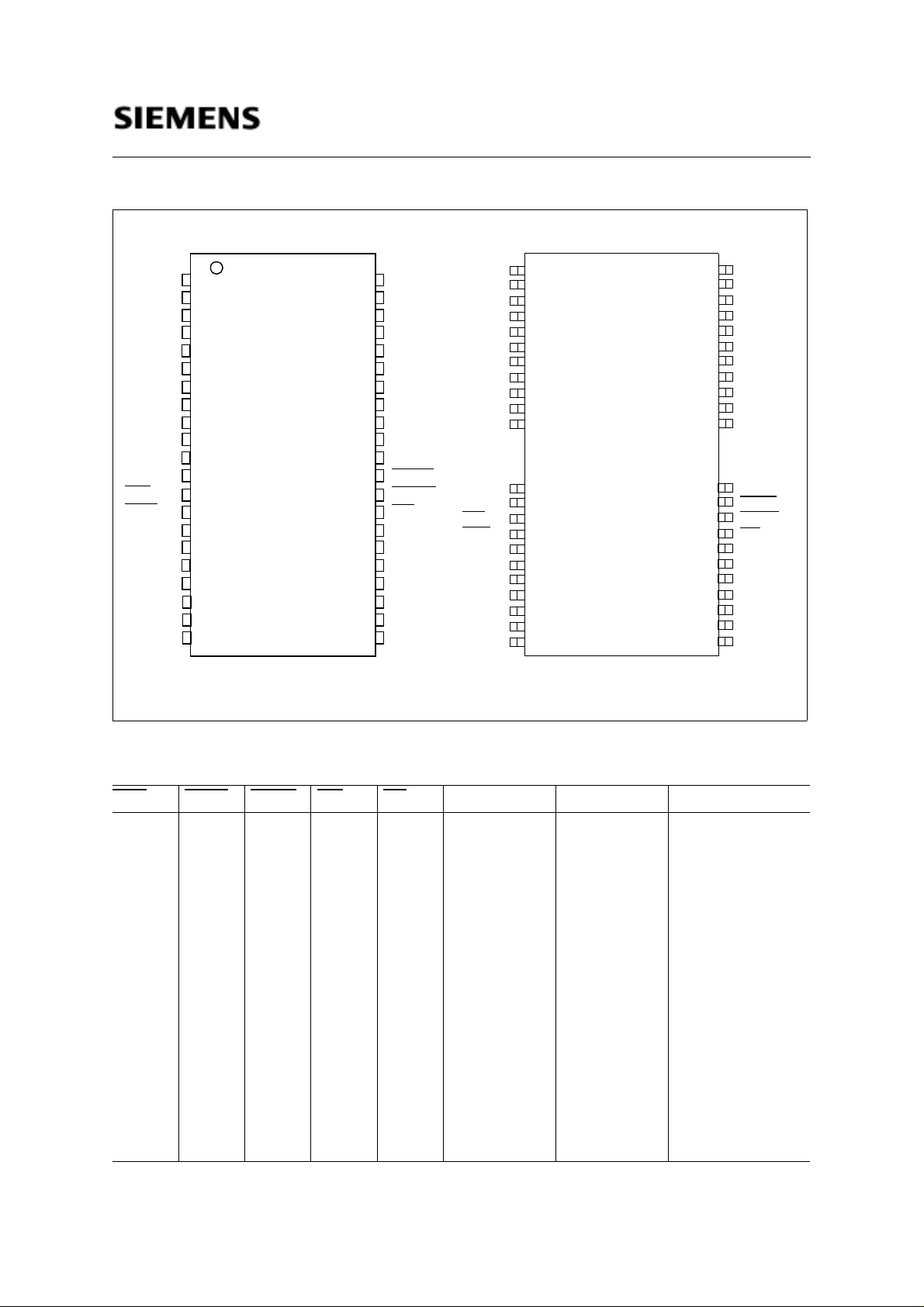
P-SOJ-42 (400 mil)
1
2
3
4
5
6
7
8
9
10
11
12
13
14
15
16
17
18
19
20
21
Vcc
I/O1
I/O2
I/O3
I/O4
Vcc
I/O5
I/O6
I/O7
I/O8
N.C.
N.C.
WE
RAS
A11/NC
A10/NC
A0
A1
A2
A3
Vcc
42
41
40
39
38
37
36
35
34
33
32
31
30
29
28
27
26
25
24
23
22
Vss
I/O16
I/O15
I/O14
I/O13
Vss
I/O12
I/O11
I/O10
I/O9
N.C.
LCAS
UCAS
OE
A9
A8
A7
A6
A5
A4
Vss
Vcc
I/O1
I/O2
I/O3
I/O4
Vcc
I/O5
I/O6
I/O7
I/O8
N.C.
N.C.
N.C.
WE
RAS
A11/N.C.
A10.N.C.
A0
A1
A2
A3
Vcc
1
2
3
4
5
6
7
8
9
10
11
15
16
17
18
19
20
21
22
23
24
25
50
49
48
47
46
45
44
43
42
41
40
36
35
34
33
32
31
30
29
28
27
26
Vss
I/O16
I/O15
I/O14
I/O13
Vss
I/O12
I/O11
I/O10
I/O9
N.C.
N.C.
LCAS
UCAS
OE
A9
A8
A7
A6
A5
A4
Vss
P-TSOPII-50/44 (400mil)
*) A11 and A10 are not connected for HYB3118160BSJ/BST (1k-refresh version)
Semiconductor Group 4
HYB3116(8)160BSJ/BST(L)-50/-60/-70
3.3V 1M x 16-DRAM
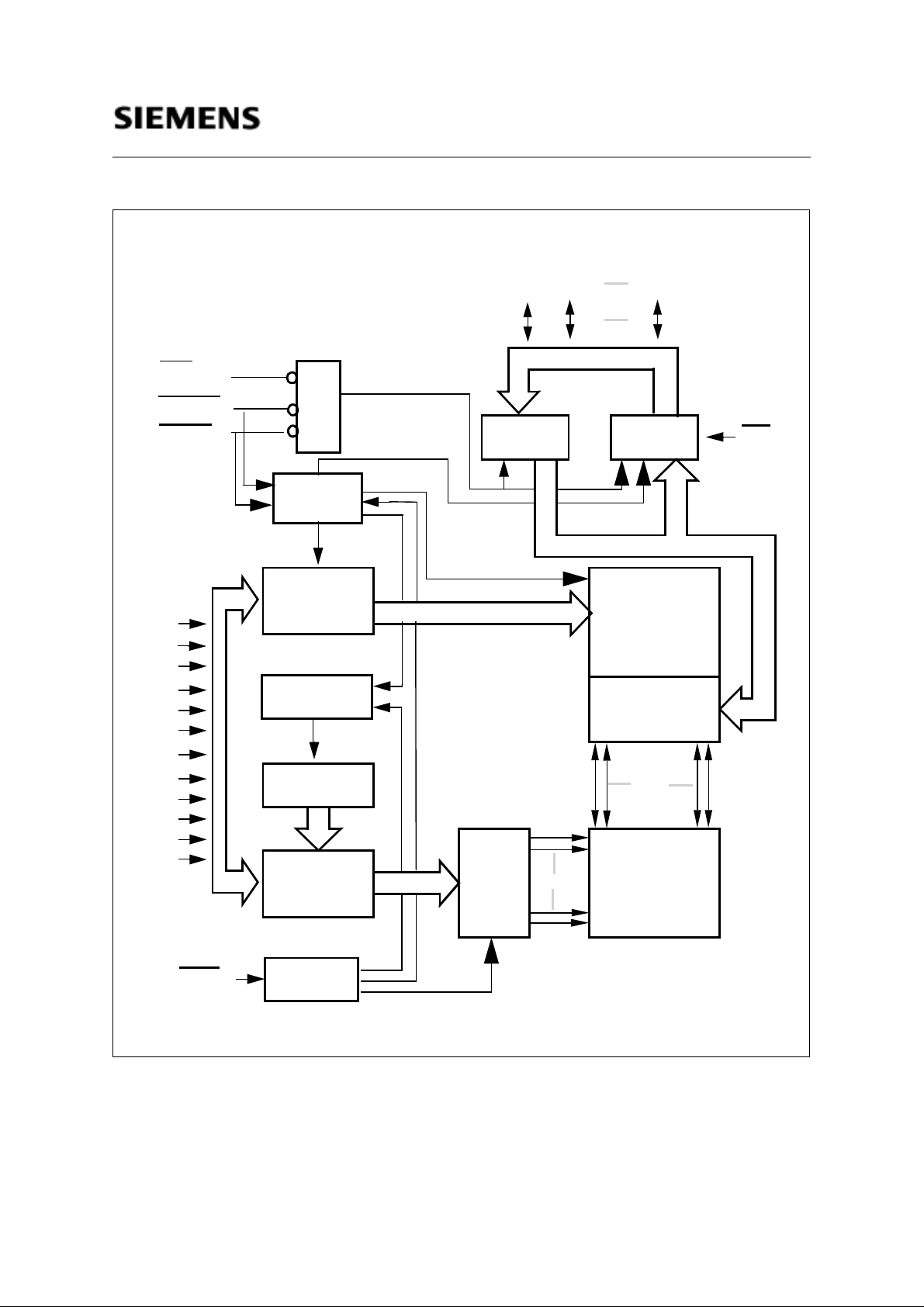
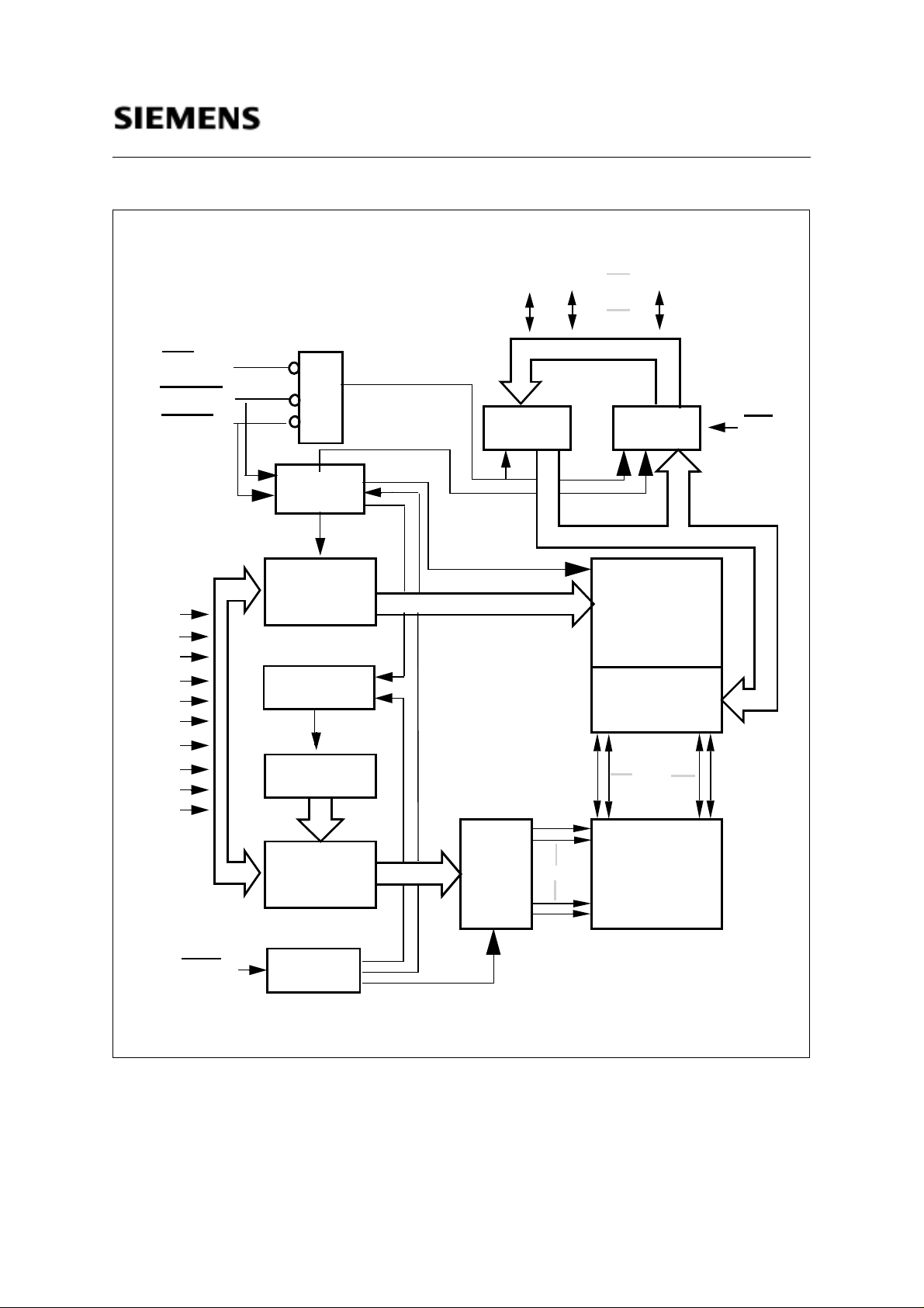
Block Diagram for HYB 3116160BSJ
No. 2 Clock
Generator
Column
Address
Buffer(8)
Refresh
Controller
Refresh
Counter (12)
Address
Buffers(12)
Row
No. 1 Clock
Generator
&
Data in
Buffer
Data out
Buffer
Column
Decoder
Sense Amplifier
I/O Gating
Memory Array
4096x256x16
Row
Decoder
A0
A1
A2
A3
A4
A5
A6
A7
A8
A9
WE
UCAS
4096
256
x16
.
RAS
8
12
16
I/O1 I/O2
OE
12 12
A10
A11
16
16
8
I/O16
LCAS
.
Semiconductor Group 5
HYB3116(8)160BSJ/BST(L)-50/-60/-70
3.3V 1M x 16-DRAM
Block Diagram for HYB 3118160BSJ
No. 2 Clock
Generator
Column
Address
Buffer(10)
Refresh
Controller
Refresh
Counter (10)
Address
Buffers(10)
Row
No. 1 Clock
Generator
&
Data in
Buffer
Data out
Buffer
Column
Decoder
Sense Amplifier
I/O Gating
Memory Array
1024x1024x16
Row
Decoder
A0
A1
A2
A3
A4
A5
A6
A7
A8
A9
WE
UCAS
1024
1024
x16
.
RAS
10
10
16
I/O1 I/O2
OE
10 10
16
16
10
I/O16
LCAS
.
Semiconductor Group 6
HYB3116(8)160BSJ/BST(L)-50/-60/-70
3.3V 1M x 16-DRAM
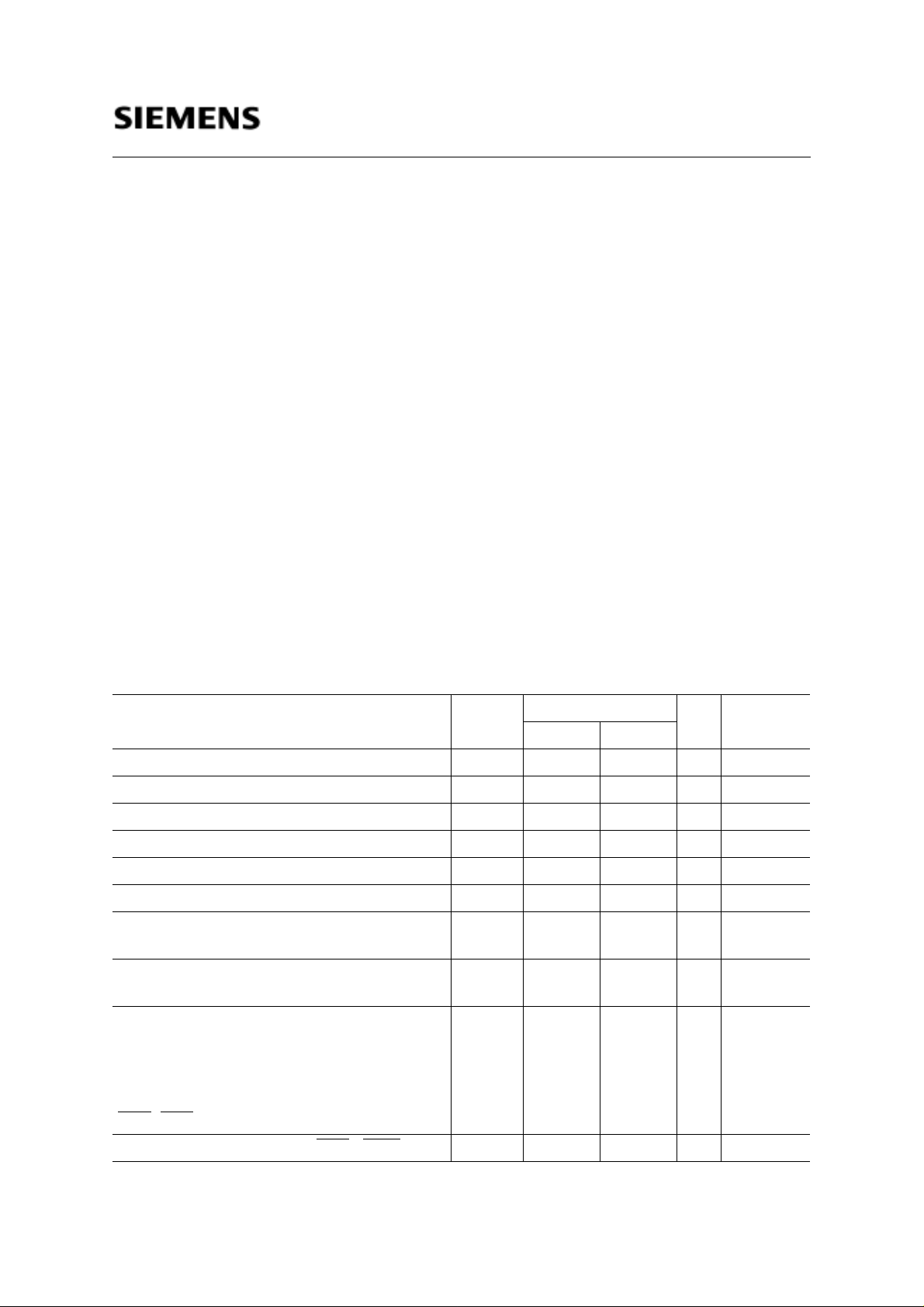
Absolute Maximum Ratings
Operating temperature range .......................................... ............ ............ ................... .......0 to 70 °C
Storage temperature range.................................... ........ ........ ........ ........ ........... ........ ..– 55 to 150 °C
Soldering time..................................................................................................................... ........10 s
Input/output volt age..................... .... .. .... .... .... .... .... .. .... .... .... .... .. .... .... .... .-0.5 to min (Vcc+0.5,4.6) V
Power supply voltage....................... .............. .............. ............ .............. ................... ..-0.5 V to 4.6 V
Power dissipation..................... ...... ...... .... ...... ...... ...... ...... ...... ...... .... ...... ......... ...... ...... ...... .... ...1.0 W
Data out current (short circuit)................................................................................................50 mA
Note:
Stresses above those list ed under “Absolute M aximum Ratings ” ma y cause permanent damage of
the device. Exposure to absolute maximum rating conditions for extended periods may affect device
reliability.
DC Characteristics (values in brackets for HYB3116160BSJ)
T
A
= 0 to 70 °C, V
SS
= 0 V, V
CC
= 3.3 V ± 0.3 V, t
T
= 5 ns
Parameter Symbol Limit Values Unit Test
Condition
min. max.
Input high voltage
V
IH
2.0 Vcc+0.5 V
1)
Input low voltage V
IL
– 0.5 0.8 V
1)
TTL Output high voltage (I
OUT
= – 2 mA) V
OH
2.4 – V
1)
TTL Output low voltage (I
OUT
= 2 mA) V
OL
– 0.4 V
1)
CMOS Output high voltage (I
OUT
= – 100 µA) V
OH
Vcc-0.2 – V
1)
CMOS Output low voltage (I
OUT
= 100 µA) V
OL
– 0.2 V
1)
Input leakage current,any input
(0 V ≤
V
IH
≤ Vcc + 0.3V, all other pins = 0 V)
I
I(L)
– 10 10 µA
1)
Output leakage current
(DO is disabled, 0 V ≤
V
OUT
≤ Vcc + 0.3V)
I
O(L)
– 10 10 µA
1)
Average V
CC
supply current:
-50 ns version
-60 ns version
-70 ns version
(RAS
, CAS, address cycling, t
RC
= t
RC
min.)
I
CC1
–
–
–
200(100)
180 (90)
160 (80)
mA
mA
mA
2) 3) 4)
2) 3) 4)
2) 3) 4)
Standby V
CC
supply current (RAS =CAS= V
IH
) I
CC2
–2mA–
Semiconductor Group 7
HYB3116(8)160BSJ/BST(L)-50/-60/-70
3.3V 1M x 16-DRAM
Average
V
CC
supply current, during RAS-only
refresh cycles: -50 ns version
-60 ns version
-70 ns version
(RAS
cyc ling: CAS = V
IH
, t
RC
= t
RC
min.)
I
CC3
–
–
–
200(100)
180 (90)
160 (80)
mA
mA
mA
2) 4)
2) 4)
2) 4)
Average V
CC
supply current,
during fast page mode: -50 ns version
-60 ns version
-70 ns version
(RAS
= V
IL
, CAS, address cycling, t
PC
= t
PC
min.)
I
CC4
–
–
–
55 (40)
50 (35)
45 (30)
mA
mA
mA
2) 3) 4)
2) 3) 4)
2) 3) 4)
Standby V
CC
supply current
(RAS
= CAS = V
CC
– 0.2 V)
I
CC5
–1mA
1)
Standby V
CC
supply current (L-version)
(RAS
= CAS = V
CC
– 0.2 V)
I
CC5
– 200 µA
1)
Average V
CC
supply current, during CAS-
before-RAS refresh mode: -50 ns version
-60 ns version
-70 ns version
(RAS
, CAS cycling, t
RC
= t
RC
min.)
I
CC6
–
–
–
200(100)
180 (90)
160 (80)
mA
mA
mA
2) 4)
2) 4)
2) 4)
Average Self Refresh Current
(CBR cycle with tRAS>TRASSmin., CAS held low,
WE
=Vcc-0.2V, Address and Din=Vcc--0.2V or 0.2V)
I
CC7
_1
250
mA
µA L-version
Capacitance
T
A
= 0 to 70 °C,V
CC
= 3.3 V ± 0.3 V, f = 1 MHz
Parameter Symbol Limit Values Unit
min. max.
Input capacitance (A0 to A11)
C
I1
–5pF
Input capacitance (RAS
, UCAS, LCAS, WE, OE) C
I2
–7pF
I/O capacitance (I/O1-I/O16)
C
IO
–7pF
DC Characteristics (values in brackets for HYB3116160BSJ)
(cont’d)
T
A
= 0 to 70 °C, V
SS
= 0 V, V
CC
= 3.3 V ± 0.3 V, t
T
= 5 ns
Parameter Symbol Limit Values Unit Test
Condition
min. max.
Semiconductor Group 8
HYB3116(8)160BSJ/BST(L)-50/-60/-70
3.3V 1M x 16-DRAM
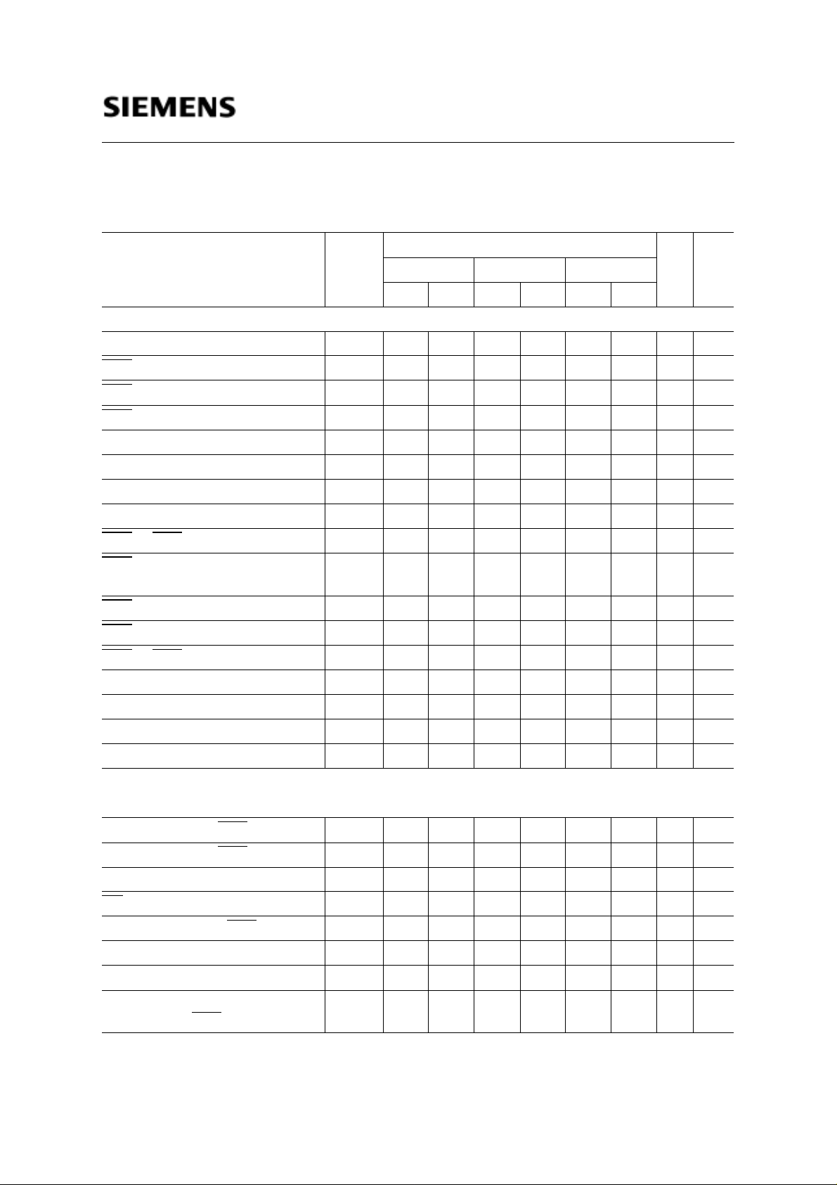
AC Characteristics
5)6)
16F
T
A
= 0 to 70 °C,V
CC
= 3.3 V ± 0.3 V, t
T
= 5 ns
Parameter
Symbol
Limit Values
Unit Note
-50 -60 -70
min. max. min. max. min. max.
common parameters
Random read or write cycle time t
RC
90 – 110 – 130 – ns
RAS
precharge time t
RP
30 – 40 – 50 – ns
RAS
pulse width t
RAS
50 10k 60 10k 70 10k ns
CAS
pulse width t
CAS
13 10k 15 10k 20 10k ns
Row address setup time t
ASR
0–0–0–ns
Row address hold time t
RAH
8 – 10 – 10 – ns
Column address setup time t
ASC
0–0–0–ns
Column address hold time t
CAH
10 – 15 – 15 – ns
RAS
to CAS delay time t
RCD
18 37 20 45 20 50
RAS
to column address delay
time
t
RAD
13 25 15 30 15 35 ns
RAS
hold time t
RSH
13 15 – 20 – ns
CAS
hold time t
CSH
50 60 – 70 – ns
CAS
to RAS precharge time t
CRP
5–5–5–ns
Transition time (rise and fall) t
T
350350350ns7
Refresh period for HYB3118160 t
REF
– 16 – 16 – 16 ms
Refresh period for HYB3116160 t
REF
– 64 – 64 – 64 ms
Refresh period for L-versions t
REF
– 256 – 256 – 256 ms
Read Cycle
Access time from RAS t
RAC
– 50 – 60 – 70 ns 8, 9
Access time from CAS
t
CAC
– 13 – 15 – 20 ns 8, 9
Access time from colum n address t
AA
– 25 – 30 – 35 ns 8,10
OE
access time t
OEA
– 13 – 15 – 20 ns
Column address to RAS
lead time t
RAL
25 – 30 – 35 – ns
Read command setup time t
RCS
0–0–0–ns
Read command hold time t
RCH
0–0–0–ns11
Read command hold time
referenced to RAS
t
RRH
0–0–0–ns11
 Loading...