


HYB3164805BJ-40
Siemens HYB3164805BJ-40, HYB3164805BJ-50, HYB3164805BJ-60, HYB3164805BT-40, HYB3164805BT-50 Datasheet
...
8M x 8-Bit Dynamic RAM
(4k & 8k Refresh, EDO-version)
Premininary Information
• 8 388 608 words by 4-bit organization
• 0 to 70 °C operating temperature
• Hyper Page Mode - EDO - operation
• Performance:
t
RAC
t
CAC
t
AA
t
RC
t
HPC
RAS access time 40 50 60 ns
CAS access time 10 13 15 ns
Access time from address 20 25 30 ns
Read/write cycle time 69 84 104 ns
Hyper page mode (EDO)
cycle time
HYB 3164805BJ/BT(L) -40/-50/-60
HYB 3165805BJ/BT(L) -40/-50/-60
-40 -50 -60
16 20 25 ns
• Single + 3.3 V (± 0.3V) power supply
• Low power dissipation:
max. 306 active mW ( HYB 3164805BJ/BT(L)-40)
max. 252 active mW ( HYB 3164805BJ/BT(L)-50)
max. 216 active mW ( HYB 3164805BJ/BT(L)-60)
max. 486 active mW ( HYB 3165805BJ/BT(L)-40)
max. 396 active mW ( HYB 3165805BJ/BT(L)-50)
max. 324 active mW ( HYB 3165805BJ/BT(L)-60)
7.2 mW standby (LVTTL)
3.6 mW standby (LVMOS)
720 µA standby for L-version
• Read, write, read-modify-write, CAS-before-RAS refresh (CBR),
RAS
-only refresh, hidden refresh
• Self refresh (L-version only)
• 8192 refresh cycles/128 ms , 13 R/ 10C addresses (HYB 3164805BJ/BT)
4096 refresh cycles/ 64 ms , 12 R/ 11C addresses (HYB 3165805BJ/BT)
• 128 msec refresh period for L-versions
• Plastic Package: P-SOJ-32-1 400 mil HYB 3164(5)400BJ
P-TSOPII-32-1 400 mil HYB 3164(5)400BT(L)
Semiconductor Group 1 12.97
HYB3164(5)805BJ/BT(L)-40/-50/-60
8M x 8-DRAM
This HYB3164(5)805B is a 64 MBit dynamic RAM organized 8 388 608 by 8 bits. The device is
fabricated in SIEMENS’ most advanced 0,25 µm-CMOS silicon gate process technology. The circuit
and process design allow this device to achieve high performance and low power dissipation. The
HYB3164(5)805B operates with a single 3.3 +/-0.3V power supply and interfaces with either LVTTL
or LVCMOS levels. Multiplexed address inputs permit the HYB 3164(5)400B to be packaged in a
400mil wide SOJ-32 or TSOP-32 plastic package. These packages provide high system bit
densities and are compatible with commonly used automatic testing and insertion equipment.The
HYB3164(5)805BTL parts have a very low power „sleep mode“ supported by Self Refresh.
Ordering Information
Type Ordering
Code
8k-refresh versions:
HYB 3164805BJ-40 P-SOJ-32-1 400 mil DRAM (access time 40 ns)
HYB 3164805BJ-50 P-SOJ-32-1 400 mil DRAM (access time 50 ns)
HYB 3164805BJ-60 P-SOJ-32-1 400 mil DRAM (access time 60 ns)
HYB 3164805BT-40 P-TSOPII-32-1 400 mil DRAM (access time 40 ns)
HYB 3164805BT-50 P-TSOPII-32-1 400 mil DRAM (access time 50 ns)
HYB 3164805BT-60 P-TSOPII-32-1 400 mil DRAM (access time 60 ns)
HYB 3164805BTL-50 P-TSOPII-32-1 400 mil DRAM (access time 50 ns)
HYB 3164805BTL-60 P-TSOPII-32-1 400 mil DRAM (access time 60 ns)
4k-refresh versions:
HYB 3165805BJ-40 P-SOJ-32-1 400 mil DRAM (access time 40 ns)
HYB 3165805BJ-50 P-SOJ-32-1 400 mil DRAM (access time 50 ns)
HYB 3165805BJ-60 P-SOJ-32-1 400 mil DRAM (access time 60 ns)
HYB 3165805BT-40 P-TSOPII-32-1 400 mil DRAM (access time 40 ns)
HYB 3165805BT-50 P-TSOPII-32-1 400 mil DRAM (access time 50 ns)
Package Descriptions
HYB 3165805BT-60 P-TSOPII-32-1 400 mil DRAM (access time 60 ns)
HYB 3165805BTL-50 P-TSOPII-32-1 400 mil DRAM (access time 50 ns)
HYB 3165805BTL-60 P-TSOPII-32-1 400 mil DRAM (access time 60 ns)
Semiconductor Group 2
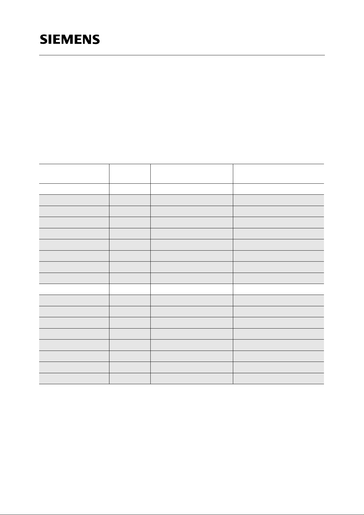
VCC
I/O1
I/O2
I/O3
I/O4
N.C.
VCC
WE
RAS
.
A0
A1
A2
A3
A4
A5
VCC
HYB3164(5)805BJ/BT(L)-40/-50/-60
P-SOJ-32-1 (400 mil)
P-TSOPII-32-1 (400 mil)
O
1
2
3
4
5
6
7
8
9
10
11
12
13
14
15
16
32
31
30
29
28
27
26
25
24
23
22
21
20
19
18
17
8M x 8-DRAM
VSS
I/O8
I/O7
I/O6
I/O5
VSS
CAS
OE
A12 / N.C. *
A11
A10
A9
A8
A7
A6
VSS
* Pin 24 is A12 for HYB 3164805BJ/BT(L) and N.C. for HYB 3165805BJ/BT(L)
Pin Configuration
Pin Names
A0-A12 Address Inputs for 8k-refresh version HYB 3164805BJ/BT(L)
A0-A11 Address Inputs for 4k-refresh version HYB 3165805BJ/BT(L)
RAS
OE
I/O1-I/O8 Data Input/Output
CAS
WE
Vcc Power Supply ( + 3.3V)
Vss Ground
Row Address Strobe
Output Enable
Column Address Strobe
Read/Write Input
Semiconductor Group 3
TRUTH TABLE
HYB3164(5)805BJ/BT(L)-40/-50/-60
8M x 8-DRAM
FUNCTION RAS CAS WE OE ROW
ADDR
Standby H H - X X X X X High Impedance
Read L L H L ROW COL Data Out
Early-Write L L L X ROW COL Data In
Delayed-Write L L H - L H ROW COL Data In
Read-Modify-Write L L H - L L - H ROW COL Data Out, Data In
Hyper Page Mode Read 1st Cycle L H - L H L ROW COL Data Out
2nd Cycle L H - L H L n/a COL Data Out
Hyper Page Mode Write 1st Cycle L H - L L X ROW COL Data In
2nd Cycle L H - L L X n/a COL Data In
Hyper Page Mode RMW 1st Cycle L H - L H - L L - H ROW COL Data Out, Data In
2st Cycle L H - L H - L L - H n/a COL Data Out, Data In
RAS only refresh L H X X ROW n/a High Impedance
CAS-before-RAS refresh H - L L H X X n/a High Impedance
Test Mode Entry H - L L L X X n/a High Impedance
Hidden Refresh READ L-H-L L H L ROW COL Data Out
WRITE L-H-L L L X ROW COL Data In
Self Refresh
(L-version only)
H - L L H X X X High Impedance
COL
ADDR
I/O1-
I/O4
Semiconductor Group 4
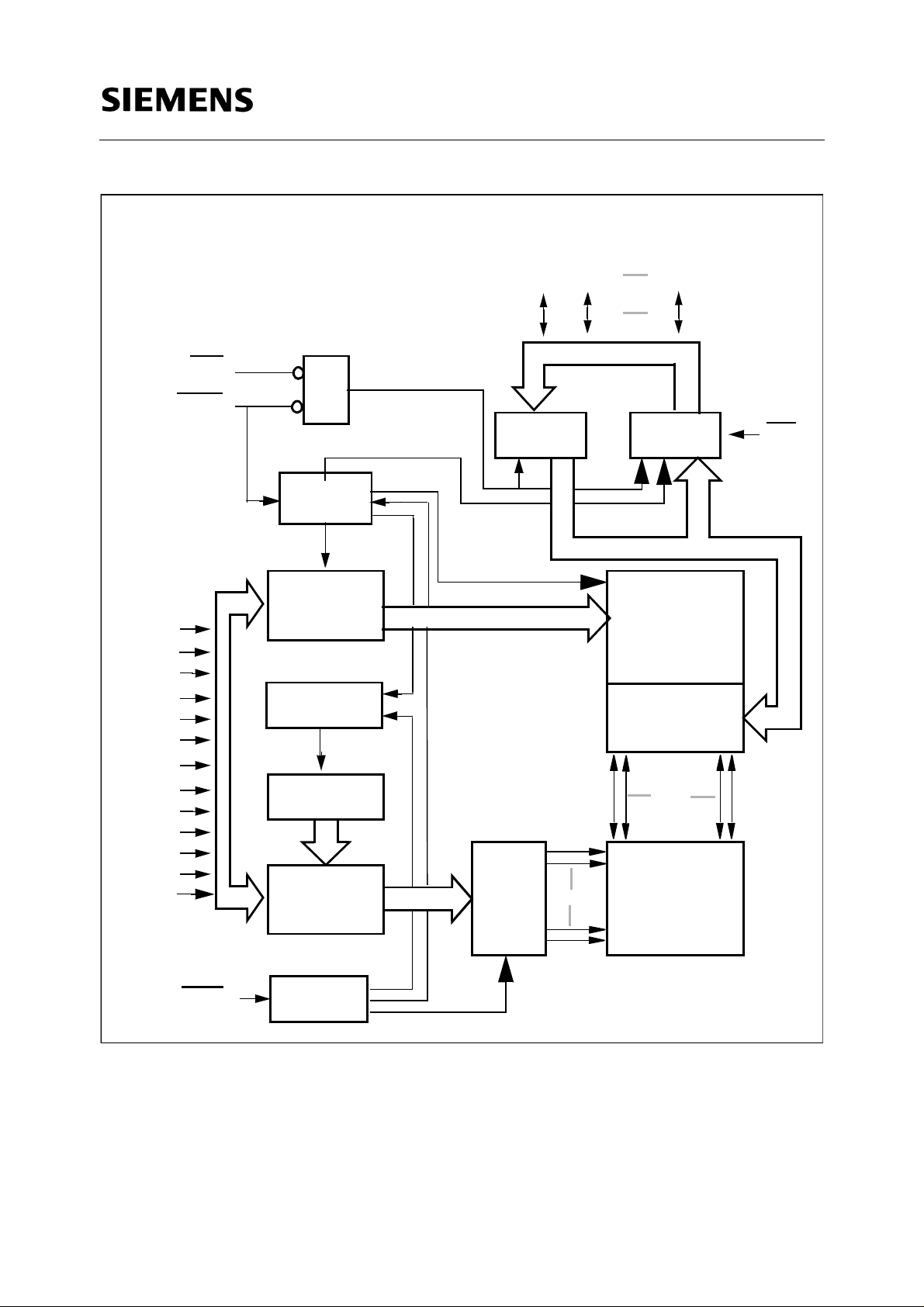
HYB3164(5)805BJ/BT(L)-40/-50/-60
8M x 8-DRAM
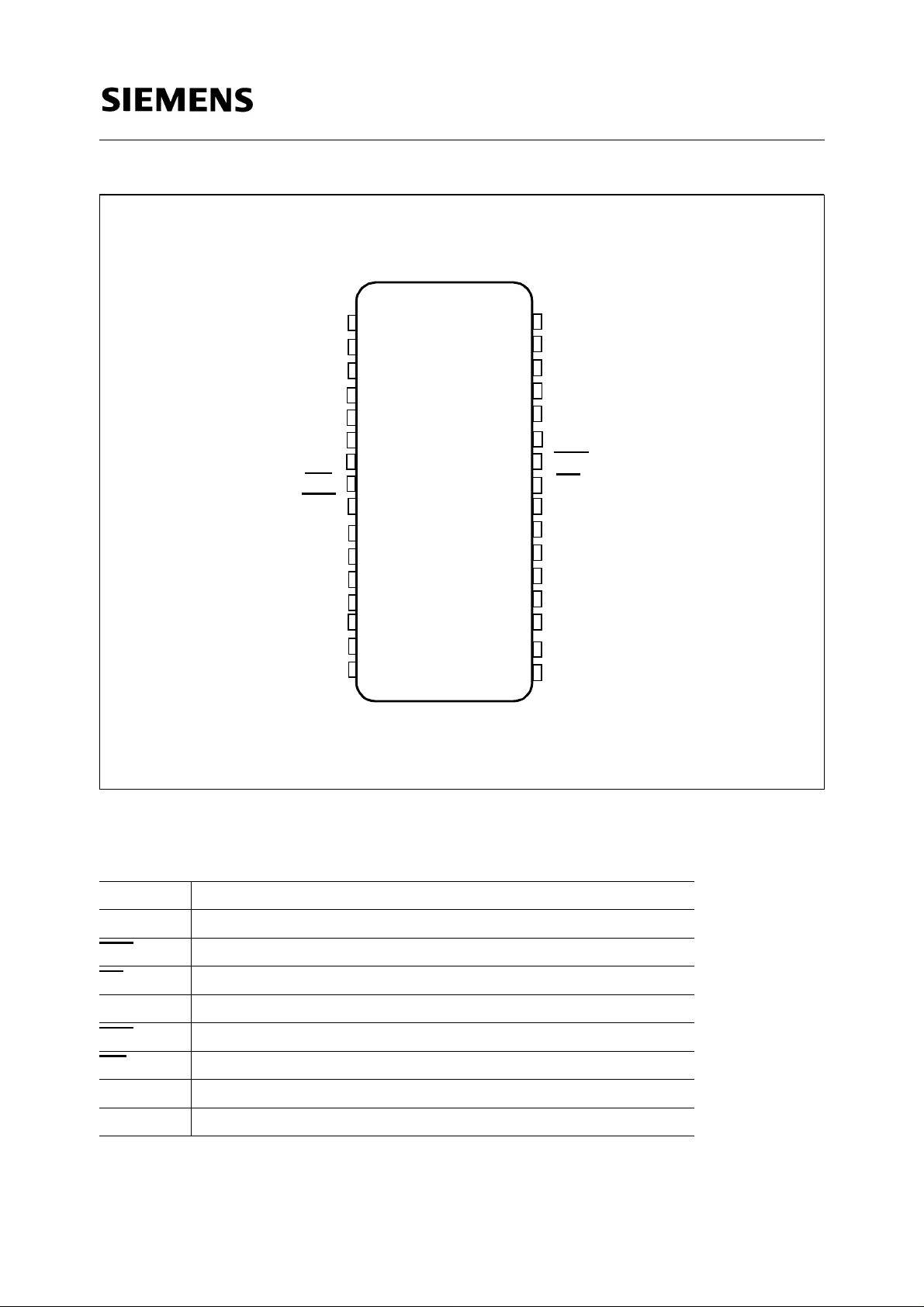
WE
CAS
A0
A1
A2
A3
A4
A5
A6
A7
A8
A9
A10
A11
A12
.
10
13 13
&
No. 2 Clock
Generator
Column
Address
Buffer(10)
Refresh
Controller
Refresh
Counter (13)
13
Row
Address
Buffers(13)
I/O1 I/O2
Data in
Buffer
Row
Decoder
8
10
8192
I/O8
Data out
Buffer
8
Column
Decoder
Sense Amplifier
I/O Gating
1024
x8
Memory Array
8192 x 1024 x 8
OE
8
RAS
Block Diagram for HYB 3164805BJ/BT(L)
Semiconductor Group 5
No. 1 Clock
Generator
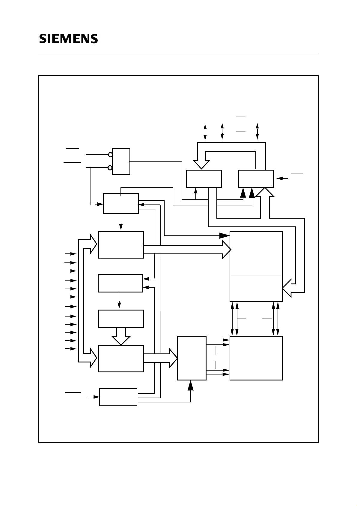
HYB3164(5)805BJ/BT(L)-40/-50/-60
8M x 8-DRAM
A0
A1
A2
A3
A4
A5
A6
A7
A8
A9
A10
A11
WE
CAS
.
11
12 12
&
No. 2 Clock
Generator
Column
Address
Buffer(11)
Refresh
Controller
Refresh
Counter (12)
12
Row
Address
Buffers(12)
I/O1 I/O2
Data in
Buffer
Row
Decoder
8
11
4096
I/O8
Data out
Buffer
8
Column
Decoder
Sense Amplifier
I/O Gating
2048
x8
Memory Array
4096 x 2048 x 8
OE
8
RAS
Block Diagram for HYB 3165805BJ/BT(L)
Semiconductor Group 6
No. 1 Clock
Generator
HYB3164(5)805BJ/BT(L)-40/-50/-60
8M x 8-DRAM
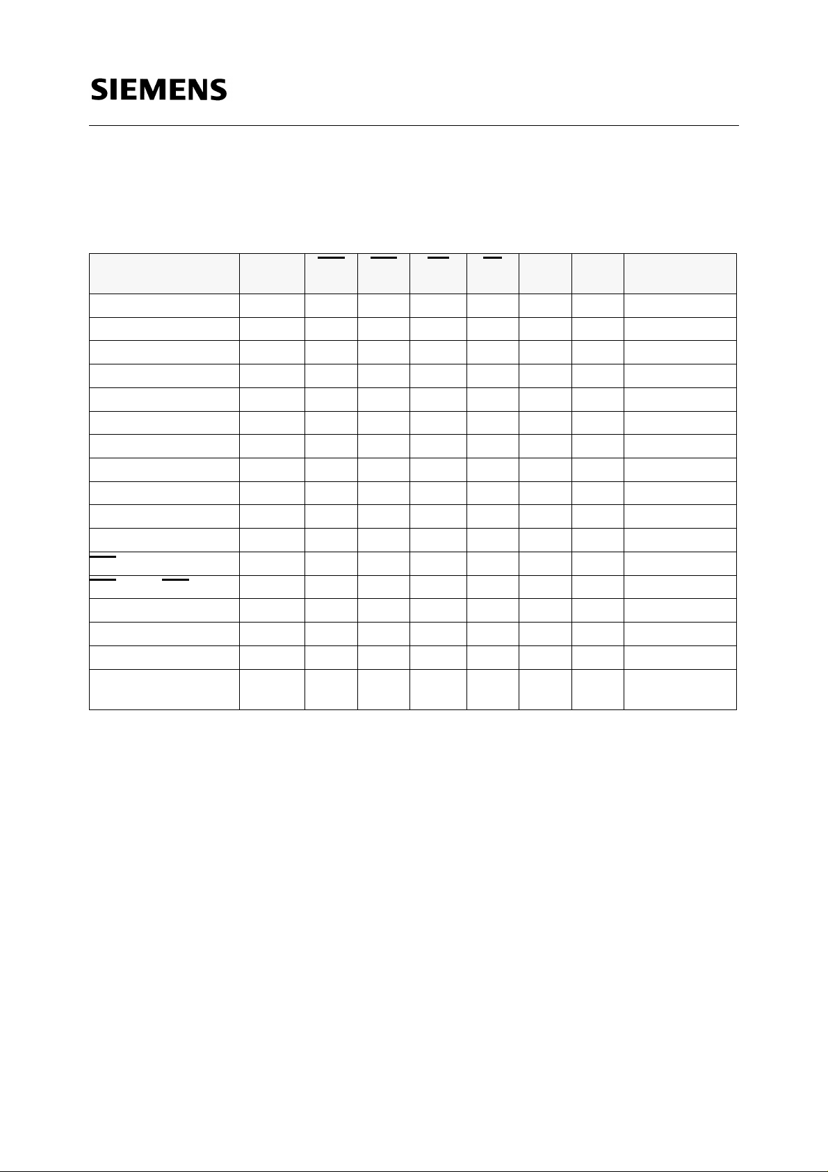
Absolute Maximum Ratings
Operating temperature range.............................................................................................. 0 to 70 °C
Storage temperature range......................................................................................... – 55 to 150 °C
Input/output voltage.................................................................................. -0.5 to min (Vcc+0.5,4.6) V
Power supply voltage.................................................................................................... -0.5V to 4.6 V
Power dissipation............................................................................................................... .....0.62 W
Data out current (short circuit)................................................................................................ ..50 mA
Note
Stresses above those listed under „Absolute Maximum Ratings“ may cause permanent damage of
the device. Exposure to absolute maximum rating conditions for extended periods may effect device
reliability.
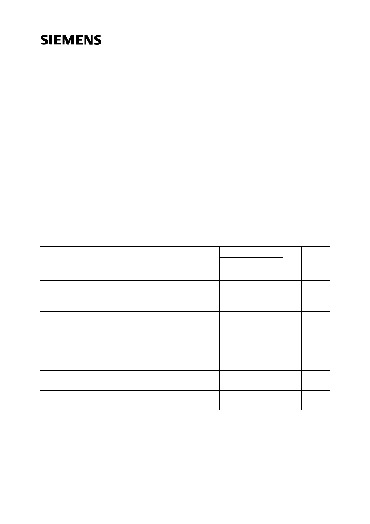
DC Characteristics
T
= 0 to 70 °C, VSS = 0 V, VCC = 3.3 V ± 0.3 V
A
Parameter Symbol Limit Values Unit Note
min. max.
Input high voltage
Input low voltage
Output high voltage (LVTTL)
V
IH
V
IL
V
OH
2.0 Vcc+0.3 V 1)
– 0.3 0.8 V 1)
2.4 – V
Output „H“ level voltage (Iout = -2mA)
Output low voltage (LVTTL)
V
OL
–0.4V
Output „L“level voltage (Iout = +2mA)
Output high voltage (LVCMOS)
V
OH
Vcc-0.2 - V
Output „H“ level voltage (Iout = -100uA)
Ouput low voltage (LVCMOS)
V
OL
- 0.2 V
Output „L“ level voltage (Iout = +100uA)
Input leakage current,any input
(0 V < Vin < Vcc , all other pins = 0 V
Output leakage current
(DO is disabled, 0 V < Vout < Vcc )
I
I
I(L)
O(L)
– 2 2 µA
– 2 2 µA
Semiconductor Group 7

HYB3164(5)805BJ/BT(L)-40/-50/-60
8M x 8-DRAM
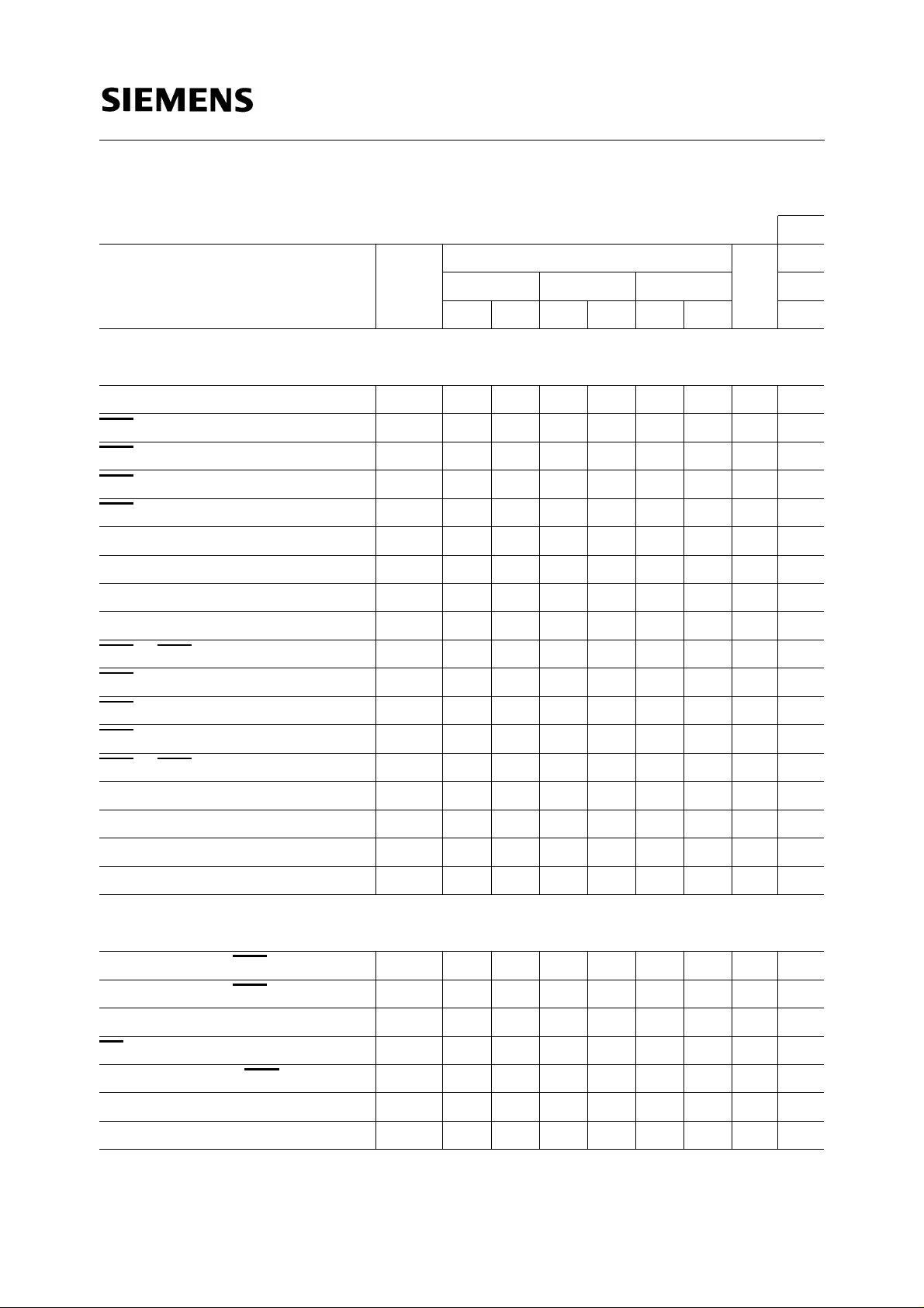
DC-Characteristics (cont’d)
T
= 0 to 70 °C, VSS = 0 V, VCC = 3.3 V ± 0.3 V
A
Parameter Symbol refresh version Unit Note
4k row 8k row
Operating Current
-40 ns version
-50 ns version
- -60 ns version
(RAS, CAS, address cycling: tRC = tRC min.)
Standby Current (
Only Refresh Current:
RAS
RAS=CAS= Vih) I
- -40 ns version
-50 ns version
-60 ns version
(RAS cycling: CAS = VIH: tRC = tRC min.)
Hyper Page Mode (EDO) Current:
-40 ns version
-50 ns version
-60 ns version
(RAS = VIL, CAS, address cycling: tHPC=tHPC min.)
Standby Current (
RAS=CAS= Vcc-0.2V) I
Standby Current (L-Version)
(RAS=CAS= Vcc-0.2V)
Before RAS Refresh Current
CAS
-40 ns version
-50 ns version
-60 ns version
(RAS, CAS cycling: tRC = tRC min.)
I
I
I
I
I
CC1
CC2
CC3
CC4
CC5
CC5
CC6
2) 3) 4)
135
110
90
85
70
60
mA
mA
mA
22mA–
2) 4)
135
110
90
100
65
45
85
70
60
100
65
45
mA
mA
mA
mAmA2) 3) 4)
11mA–
200 200 µA–
135
110
90
85
70
60
mAmA2) 4)
Self Refresh Current (L-version only)
(CBR cycle with tRAS>TRASSmin, CAS held low,
WE
= Vcc-0.2V, Address and Din=Vcc-0.2V or 0.2V)
I
CC7
400 400 µA
Capacitance
T
= 0 to 70 °C,VCC = 3.3 V ± 0.3 V, f = 1 MHz
A
Parameter Symbol Limit Values Unit
min. max.
Input capacitance (A0 to A11,A12)
Input capacitance (RAS
, CAS, WE, OE) C
I/O capacitance (I/O1-I/O8)
C
I1
I2
C
IO
–5pF
–7pF
–7pF
Semiconductor Group 8
HYB3164(5)805BJ/BT(L)-40/-50/-60
8M x 8-DRAM
AC Characteristics
T
= 0 to 70 °C,VCC = 3.3 V ± 0.3V , tT = 2 ns
A
5)6)
Parameter
Common Parameters
Random read or write cycle time t
pulse width t
RAS
pulse width t
CAS
precharge time t
RAS
precharge time t
CAS
Row address setup time t
Row address hold time t
Column address setup time t
Column address hold time t
to CAS delay time t
RAS
to column address delay time t
RAS
hold time t
RAS
hold time t
CAS
to RAS precharge time t
CAS
Transition time (rise and fall) t
Refresh period for 8k-refresh-version t
Refresh period for 4k-refresh version t
Refresh period for L-versions t
Symbol
RC
RAS
CAS
RP
CP
ASR
RAH
ASC
CAH
RCD
RAD
RSH
CSH
CRP
T
REF
REF
REF
AC64-2E
Limit Values
Unit Note
- 40 - 50 - 60
min. max. min. max. min. max.
69 – 84 – 104 – ns
40
6
100k
100k
50
8
100k
100k
60
10
100k
100k
ns
ns
25 – 30 – 40 – ns
6–8–10–ns
0–0–0–ns
5–7–10–ns
0–0–0–ns
5–7–10–ns
9 3011371445ns
7 20 9 25 12 30 ns
6–8 10–ns
32 – 40 48 – ns
5–5–5–ns
150150150ns7
– 128 – 128 – 128 ms
–64–64–64ms
– 128 – 128 – 128 ms
Read Cycle
Access time from RAS t
Access time from CAS
Access time from column address t
access time t
OE
Column address to RAS
lead time t
Read command setup time t
Read command hold time t
RAC
t
CAC
AA
OEA
RAL
RCS
RCH
Semiconductor Group 9
–40–50–60ns8, 9
–10–13–15ns8, 9
– 20 – 25 – 30 ns 8,10
–10–13–15ns
20 – 25 – 30 – ns
0–0–0–ns
0–0–0–ns11
 Loading...