


Siemens HYB314171BJ-50, HYB314171BJ-60, HYB314171BJ-70, HYB314171BJL-50, HYB314171BJL-60 Datasheet
...3.3V 256 K x 16-Bit Dynamic RAM
3.3V Low Power 256 K x 16-Bit Dynamic RAM with Self Refresh
Preliminary Information
•262 144 words by 16-bit organization
•0 to 70 °C operating temperature
•Fast access and cycle time
•RAS access time: 50 ns (-50 version) 60 ns (-60 version) 70 ns (-70 version)
•CAS access time: 15ns (-50,-60 version) 20 ns (-70 version)
•Cycle time:
95 ns (-50 version)
110 ns (-60 version)
130 ns (-70 version)
•Fast page mode cycle time 35 ns (-50 version)
40 ns (-60 version)
45 ns (-70 version)
•Single + 3.3 V (± 0.3 V) supply with a builtin VBB generator
HYB 314171BJ-50/-60/-70
HYB 314171BJL-50/-60/-70
•Low Power dissipation
max. 450 mW active (-50 version) max. 378 mW active (-60 version) max. 306 mW active (-70 version)
•Standby power dissipation 7.2 mW standby (TTL)
3.6 mW max. standby (CMOS)
0.72 mW max. standby (CMOS) for Low Power Version
•Output unlatched at cycle end allows twodimensional chip selection
•Read, write, read-modify write, CAS- before-RAS refresh, RAS-only refresh, hidden-refresh and fast page mode capability
•2 CAS / 1 WE control
•Self Refresh (L-Version)
•All inputs and outputs TTL-compatible
•512 refresh cycles / 16 ms
•512 refresh cycles / 128 ms Low Power Version only
•Plastic Packages: P-SOJ-40-1 400mil width
The HYB 314171BJ/BJL is a 4 MBit dynamic RAM organized as 262 144 words by 16-bit. The HYB 314171BJ/BJL utilizes CMOS silicon gate process as well as advanced circuit techniques to provide wide operation margins, both internally and for the system user. Multiplexed address inputs permit the HYB 314171BJ/BJL to be packed in a standard plastic 400mil wide P-SOJ-40-1 package. This package size provides high system bit densities and is compatible with commonly used automatic testing and insertion equipment. System oriented features include Self Refresh (L- Version), single + 3.3 V (± 0.3 V) power supply, direct interfacing with high performance logic device families.
Semiconductor Group |
1 |
7.96 |

HYB 314171BJ/BJL-50/-60/-70 3.3V 256 K x 16-DRAM
Ordering Information
Type |
Ordering Code |
Package |
Description |
|
|
|
|
HYB 314171BJ-50 |
on request |
P-SOJ-40-1 |
3.3V 50ns 256 K x 16 DRAM |
|
|
|
|
HYB 314171BJ-60 |
on request |
P-SOJ-40-1 |
3.3V 60 ns 256 K x 16 DRAM |
|
|
|
|
HYB 314171BJ-70 |
on request |
P-SOJ-40-1 |
3.3V 70 ns 256 K x 16 DRAM |
|
|
|
|
HYB 314171BJL-50 |
on request |
P-SOJ-40-1 |
3.3V 50 ns 256 K x 16 DRAM |
|
|
|
|
HYB 314171BJL-60 |
on request |
P-SOJ-40-1 |
3.3V 60 ns 256 K x 16 DRAM |
|
|
|
|
HYB 314171BJL-70 |
on request |
P-SOJ-40-1 |
3.3V 70 ns 256 K x 16 DRAM |
|
|
|
|
Truth Table
|
|
|
|
|
|
|
|
|
|
|
|
|
|
|
|
|
|
|
|
|
|
|
|
RAS |
|
|
LCAS |
|
UCAS |
|
WE |
|
|
OE |
I/O1-I/O8 |
I/O9-I/O16 |
Operation |
||||||||||
|
|
|
|
|
|
|
|
|
|
|
|
|
|
|
|
|
|
|
|||||
H |
|
H |
H |
H |
|
H |
High-Z |
High-Z |
Standby |
||||||||||||||
L |
|
H |
H |
H |
|
H |
High-Z |
High-Z |
Refresh |
||||||||||||||
L |
|
L |
H |
H |
|
L |
Dout |
High-Z |
Lower byte read |
||||||||||||||
L |
|
H |
L |
H |
|
L |
High-Z |
Dout |
Upper byte read |
||||||||||||||
L |
|
L |
L |
H |
|
L |
Dout |
Dout |
Word read |
||||||||||||||
L |
|
L |
H |
L |
|
H |
Din |
Don't care |
Lower byte write |
||||||||||||||
L |
|
H |
L |
L |
|
H |
Don't care |
Din |
Upper byte write |
||||||||||||||
L |
|
L |
L |
L |
|
H |
Din |
Din |
Word write |
||||||||||||||
L |
|
L |
L |
H |
|
H |
High-Z |
High-Z |
|
||||||||||||||
|
|
|
|
|
|
|
|
|
|
|
|
|
|
|
|
|
|
||||||
Pin Names |
|
|
|
|
|
|
|
|
|
|
|
|
|
||||||||||
|
|
|
|
|
|
|
|
|
|
|
|
|
|
|
|
|
|
||||||
A0-A8 |
|
|
|
|
|
|
|
|
|
|
|
Address Inputs |
|
|
|||||||||
|
|
|
|
|
|
|
|
|
|
|
|
|
|
|
|
|
|
|
|
|
|
|
|
|
|
|
|
|
|
|
|
|
|
|
|
|
|
|
|
|
Row Address Strobe |
|
|
||||
RAS |
|
|
|
|
|
|
|
|
|
|
|
|
|
|
|
|
|||||||
|
|
|
|
|
|
|
|
|
|
|
|
|
|
|
|
|
|
|
|
|
|||
|
|
|
|
|
|
|
|
|
|
|
|
|
|
|
|
|
Column Address Strobe |
|
|
||||
UCAS, |
|
LCAS |
|
|
|
|
|
|
|
|
|
|
|||||||||||
|
|
|
|
|
|
|
|
|
|
|
|
|
|
|
|
|
|
|
|
|
|||
|
|
|
|
|
|
|
|
|
|
|
|
|
|
|
|
|
Read/Write Input |
|
|
||||
WE |
|
|
|
|
|
|
|
|
|
|
|
|
|
|
|
||||||||
|
|
|
|
|
|
|
|
|
|
|
|
|
|
|
|
|
|
|
|
||||
|
|
|
|
|
|
|
|
|
|
|
|
|
|
|
|
|
Output Enable |
|
|
||||
OE |
|
|
|
|
|
|
|
|
|
|
|
|
|
|
|
||||||||
|
|
|
|
|
|
|
|
|
|
|
|
|
|
|
|||||||||
I/O1 – I/O16 |
|
|
|
|
|
|
Data Input/Output |
|
|
||||||||||||||
|
|
|
|
|
|
|
|
|
|
|
|
|
|
|
|
|
|
||||||
VCC |
|
|
|
|
|
|
|
|
|
|
|
Power Supply (+ 3.3 V) |
|
|
|||||||||
VSS |
|
|
|
|
|
|
|
|
|
|
|
Ground (0 V) |
|
|
|||||||||
N.C. |
|
|
|
|
|
|
|
|
|
|
|
No Connection |
|
|
|||||||||
|
|
|
|
|
|
|
|
|
|
|
|
|
|
|
|
|
|
|
|
|
|
|
|
Semiconductor Group |
2 |
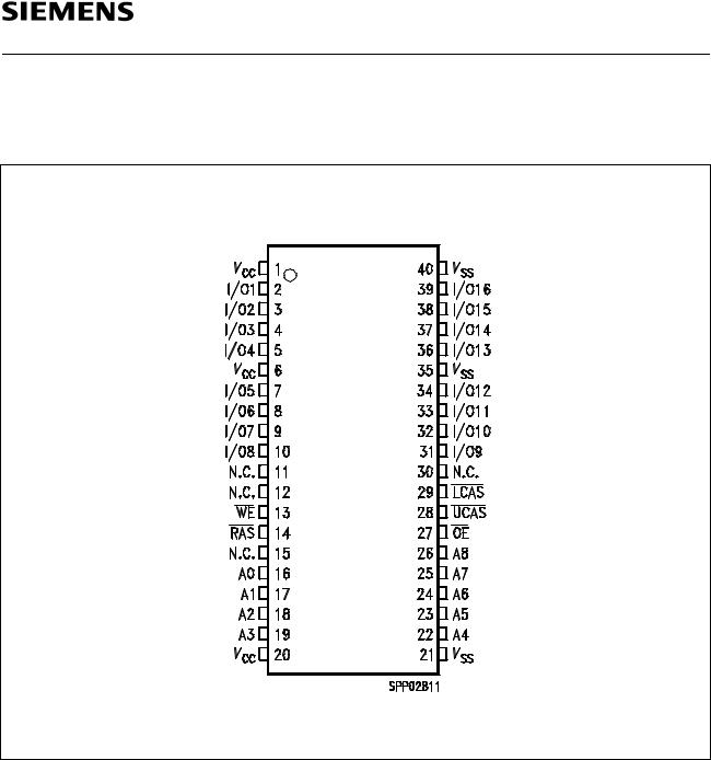
HYB 314171BJ/BJL-50/-60/-70 3.3V 256 K x 16-DRAM
Pin Configuration
(top view)
P-SOJ-40-1
Semiconductor Group |
3 |

HYB 314171BJ/BJL-50/-60/-70 |
3.3V 256 K x 16-DRAM |
Block Diagram
Semiconductor Group |
4 |

HYB 314171BJ/BJL-50/-60/-70 3.3V 256 K x 16-DRAM
Absolute Maximum Ratings |
|
|
Operating temperature range ........................................................................................ |
0 to + 70 |
°C |
Storage temperature range..................................................................................... |
– 55 to + 150 |
°C |
Input/output voltage .................................................................................... |
– 1 to (VCC + 0.5, 4.6) |
V |
Power supply voltage.................................................................................................. |
– 1 to + 4.6 |
V |
Data out current (short circuit) ................................................................................................ |
50 mA |
|
Note: Stresses above those listed under “Absolute Maximum Ratings” may cause permanent damage of the device. Exposure to absolute maximum rating conditions for extended periods may affect device reliability.
DC Characteristics
TA = 0 to 70 °C; VSS = 0 V; VCC = 3.3 V ± 0.3 V, tT = 5 ns
Parameter |
|
Symbol |
Limit Values |
Unit |
Notes |
|||||||||
|
|
|
|
|
|
|
|
|
|
|
|
|
|
|
|
|
|
|
|
|
|
|
|
|
|
min. |
max. |
|
|
|
|
|
|
|
|
|
||||||||
Input high voltage |
|
VIH |
2.0 |
VCC + 0.5 |
V |
1 |
||||||||
Input low voltage |
|
VIL |
– 1.0 |
0.8 |
V |
1 |
||||||||
LVTTL Output high voltage (IOUT = – 2.0 mA) |
VOH |
2.4 |
– |
V |
1 |
|||||||||
LVTTL Output low voltage (IOUT = 2 mA) |
VOL |
– |
0.4 |
V |
1 |
|||||||||
LVCMOS Output high voltage (IOUT = – 100 μA) |
VOH |
2.4 |
– |
V |
1 |
|||||||||
LVCMOS Output low voltage (IOUT = 100 μA) |
VOL |
– |
0.4 |
V |
1 |
|||||||||
Input leakage current, any input |
II(L) |
– 10 |
10 |
μA |
1 |
|||||||||
(0 V < VIN < VCC + 0.3 V, all other inputs = 0 V) |
|
|
|
|
|
|||||||||
|
|
|
|
|
|
|
||||||||
Output leakage current |
|
IO(L) |
– 10 |
10 |
μA |
1 |
||||||||
(DO is disabled, 0 V < VOUT < VCC + 0.3 V ) |
|
|
|
|
|
|||||||||
|
|
|
|
|
|
|
||||||||
Average VCC supply current: |
-50 version |
ICC1 |
– |
125 |
mA |
2, 3, 4 |
||||||||
|
|
|
|
|
|
|
|
|
-60 version |
|
|
105 |
|
|
|
|
|
|
|
|
|
|
|
-70 version |
|
|
85 |
|
|
|
|
|
|
|
|
|
||||||||
Standby VCC supply current |
= VIH) |
ICC2 |
– |
2 |
mA |
|
||||||||
|
(RAS |
= |
LCAS |
= |
UCAS |
= |
WE |
|
|
|
|
|
||
|
|
|
|
|
|
|||||||||
Average VCC supply current during |
ICC3 |
– |
|
|
2, 4 |
|||||||||
RAS |
-only refresh cycles: |
-50 version |
|
125 |
mA |
|
||||||||
|
|
|
|
|
|
|
|
|
-60 version |
|
|
105 |
|
|
|
|
|
|
|
|
|
|
|
-70 version |
|
|
85 |
|
|
|
|
|
|
|
|
|
|
|
|
|
|
|
|
|
Semiconductor Group |
5 |

HYB 314171BJ/BJL-50/-60/-70 3.3V 256 K x 16-DRAM
DC Characteristics (cont’d)
Parameter |
|
|
|
|
|
|
|
|
Symbol |
|
Limit Values |
Unit |
|
Notes |
|||||||||||||||||||
|
|
|
|
|
|
|
|
|
|
|
|
|
|
|
|
|
|
|
|
|
|
|
|
|
|
|
|
|
|
|
|
|
|
|
|
|
|
|
|
|
|
|
|
|
|
|
|
|
|
|
|
|
|
|
|
|
|
|
|
min. |
max. |
|
|
|
|||
|
|
|
|
|
|
|
|
|
|
|
|
||||||||||||||||||||||
Average VCC supply current during |
|
ICC4 |
– |
|
|
|
|
|
2, 3, 4 |
||||||||||||||||||||||||
fast page mode operation: |
-50 version |
|
|
|
|
70 |
|
mA |
|
|
|||||||||||||||||||||||
|
|
|
|
|
|
|
|
|
|
|
|
|
|
|
|
-60 version |
|
|
|
|
|
|
65 |
|
|
|
|
||||||
|
|
|
|
|
|
|
|
|
|
|
|
|
|
|
|
-70 version |
|
|
|
|
|
|
60 |
|
|
|
|
||||||
|
|
|
|
|
|
|
|
|
|
|
|
|
|
|
|
|
|
|
|||||||||||||||
Standby VCC supply current |
= VCC – 0.2 V) |
|
ICC5 |
– |
|
|
1 |
|
mA |
1 |
|||||||||||||||||||||||
|
(RAS |
= |
LCAS |
= |
UCAS |
= |
|
WE |
|
|
|
|
|
|
|
|
|
|
|
||||||||||||||
|
|
|
|
|
|
|
|
|
|
|
|
||||||||||||||||||||||
Average VCC supply current during |
|
|
|
– |
|
|
|
|
|
2, 4 |
|||||||||||||||||||||||
CAS |
-before- |
RAS |
refresh mode: |
|
|
|
|
|
|
|
|
|
|
|
|||||||||||||||||||
|
|
|
|
|
|
|
|
|
|
|
|
|
|
|
|
-50 version |
|
ICC6 |
|
|
|
125 |
|
mA |
|
|
|||||||
|
|
|
|
|
|
|
|
|
|
|
|
|
|
|
|
-60 version |
|
|
|
|
|
|
105 |
|
|
|
|
||||||
|
|
|
|
|
|
|
|
|
|
|
|
|
|
|
|
-70 version |
|
|
|
|
|
|
85 |
|
|
|
|
||||||
|
|
|
|
|
|
|
|
|
|
|
|
||||||||||||||||||||||
Standby VCC current (L-version) |
|
ICC5 |
– |
|
|
200 |
|
μA |
|
|
|||||||||||||||||||||||
|
|
= |
|
= |
|
|
|
= |
|
|
|
|
|
|
|
|
|
|
|
|
|
|
|
|
|
|
|
|
|||||
(RAS |
LCAS |
UCAS |
WE= VCC – 0.2 V) |
|
|
|
|
|
|
|
|
|
|
|
|||||||||||||||||||
Self Refresh Current (L-version) |
|
ICCS |
– |
|
|
250 |
|
μA |
|
|
|||||||||||||||||||||||
|
(RAS, |
|
LCAS, |
|
UCAS |
= 0.2 V |
|
|
|
|
|
|
|
|
|
|
|
|
|
|
|
|
|
|
|||||||||
A0 – A8 = VCC – 0.2 V or 0.2 V) |
|
|
|
|
|
|
|
|
|
|
|
||||||||||||||||||||||
|
|
|
|
|
|
|
|
|
|
|
|
|
|
|
|
|
|
|
|||||||||||||||
Capacitance |
|
|
|
|
|
|
|
|
|
|
|
|
|
|
|
|
|
|
|||||||||||||||
TA = 0 to 70 °C; VCC = 3.3 V ± 0.3 V, f = 1 MHz |
|
|
|
|
|
|
|
|
|
|
|||||||||||||||||||||||
|
|
|
|
|
|
|
|
|
|
|
|
|
|
|
|
||||||||||||||||||
Parameter |
|
|
|
|
|
|
|
|
|
Symbol |
|
Limit Values |
|
Unit |
|||||||||||||||||||
|
|
|
|
|
|
|
|
|
|
|
|
|
|
|
|
|
|
|
|
|
|
|
|
|
|
|
|
|
|
|
|
|
|
|
|
|
|
|
|
|
|
|
|
|
|
|
|
|
|
|
|
|
|
|
|
|
|
|
|
|
|
min. |
|
max. |
|
|
|
|
|
|
|
|
|
|
|
|
|
|
|
|
|
|
|
|
|
|
|||||||||||||||
Input capacitance (A0 to A8) |
|
|
|
|
|
|
|
|
|
CI1 |
|
|
– |
|
6 |
|
|
pF |
|||||||||||||||
Input capacitance |
|
|
|
|
|
|
|
|
|
|
|
|
|
|
|
CI2 |
|
|
– |
|
7 |
|
|
pF |
|||||||||
(RAS, |
UCAS, |
LCAS, |
WE, |
OE) |
|
|
|
|
|
||||||||||||||||||||||||
Output capacitance (l/O1 to l/O16) |
|
CIO |
|
|
– |
|
7 |
|
|
pF |
|||||||||||||||||||||||
Semiconductor Group |
6 |

HYB 314171BJ/BJL-50/-60/-70 3.3V 256 K x 16-DRAM
AC Characteristics 5)6)
TA = 0 to 70 °C; VSS = 0 V; VCC = 3.3 V ± 0.3 V, tT = 5 ns
Parameter |
Symbol |
|
|
|
Limit Values |
|
|
Unit |
Note |
||||||||||
|
|
|
|
|
|
|
|
|
|
|
|
|
|
|
|
|
|
|
|
|
|
|
|
|
|
|
|
|
|
|
|
-50 |
- 60 |
- 70 |
|
|
|||
|
|
|
|
|
|
|
|
|
|
|
|
|
|
|
|
|
|
|
|
|
|
|
|
|
|
|
|
|
|
|
min. |
|
max. |
min. |
max. |
min. |
max. |
|
|
|
|
|
|
|
|
|
|
|
|
|
|||||||||
Common Parameters |
|
|
|
|
|
|
|
|
|
|
|||||||||
|
|
|
|
|
|
|
|
|
|
|
|||||||||
Random read or write cycle time |
tRC |
95 |
|
– |
110 |
– |
130 |
– |
ns |
|
|||||||||
|
|
precharge time |
tRP |
35 |
|
– |
40 |
– |
50 |
– |
ns |
|
|||||||
RAS |
|
|
|||||||||||||||||
|
|
pulse width |
tRAS |
50 |
|
10k |
60 |
10k |
70 |
10k |
ns |
|
|||||||
RAS |
|
|
|||||||||||||||||
|
|
pulse width |
tCAS |
15 |
|
10k |
15 |
10k |
20 |
10k |
ns |
|
|||||||
CAS |
|
|
|||||||||||||||||
Row address setup time |
tASR |
0 |
|
– |
0 |
– |
0 |
– |
ns |
|
|||||||||
Row address hold time |
tRAH |
10 |
|
– |
10 |
– |
10 |
– |
ns |
|
|||||||||
Column address setup time |
tASC |
0 |
|
– |
0 |
– |
0 |
– |
ns |
|
|||||||||
Column address hold time |
tCAH |
10 |
|
– |
15 |
– |
15 |
– |
ns |
|
|||||||||
|
|
to |
|
delay time |
tRCD |
20 |
|
35 |
20 |
45 |
20 |
50 |
ns |
|
|||||
RAS |
CAS |
|
|
||||||||||||||||
|
|
to column address delay |
tRAD |
15 |
|
25 |
15 |
30 |
15 |
35 |
ns |
|
|||||||
RAS |
|
|
|||||||||||||||||
time |
|
|
|
|
|
|
|
|
|
|
|||||||||
|
|
|
|
|
|
|
|
|
|
|
|
|
|
|
|
|
|||
|
|
hold time |
tRSH |
15 |
|
– |
15 |
– |
20 |
– |
ns |
|
|||||||
RAS |
|
|
|||||||||||||||||
|
|
hold time |
tCSH |
50 |
|
– |
60 |
– |
70 |
– |
ns |
|
|||||||
CAS |
|
|
|||||||||||||||||
|
|
to |
|
precharge time |
tCRP |
5 |
|
– |
5 |
– |
5 |
– |
ns |
|
|||||
CAS |
RAS |
|
|
||||||||||||||||
Transition time (rise and fall) |
tT |
3 |
|
50 |
3 |
50 |
3 |
50 |
ns |
7 |
|||||||||
|
|
|
|
|
|
|
|
|
|
|
|||||||||
Refresh period |
tREF |
– |
|
16 |
– |
16 |
– |
16 |
ms |
|
|||||||||
Refresh period (L-version) |
tREF |
– |
|
128 |
– |
128 |
– |
128 |
ms |
|
|||||||||
Read Cycle |
|
|
|
|
|
|
|
|
|
|
|||||||||
|
|
|
|
|
|
|
|
|
|
|
|
|
|
|
|||||
Access time from |
RAS |
|
|
|
tRAC |
– |
|
50 |
– |
60 |
– |
70 |
ns |
8, 9 |
|||||
Access time from |
|
|
|
|
|
tCAC |
– |
|
15 |
– |
15 |
– |
20 |
ns |
8, 9 |
||||
CAS |
|
|
|
||||||||||||||||
Access time from column address |
tAA |
– |
|
25 |
– |
30 |
– |
35 |
ns |
8,10 |
|||||||||
|
access time |
tOEA |
– |
|
15 |
– |
15 |
– |
20 |
ns |
|
||||||||
OE |
|
|
|||||||||||||||||
Column address to |
|
|
|
lead time |
tRAL |
25 |
|
– |
30 |
– |
35 |
– |
ns |
|
|||||
RAS |
|
|
|||||||||||||||||
Read command setup time |
tRCS |
0 |
|
– |
0 |
– |
0 |
– |
ns |
|
|||||||||
Read command hold time |
tRCH |
0 |
|
– |
0 |
– |
0 |
– |
ns |
11 |
|||||||||
Read command hold time ref. to |
tRRH |
0 |
|
– |
0 |
– |
0 |
– |
ns |
11 |
|||||||||
RAS |
|
|
|
|
|
|
|
|
|
|
|
||||||||
|
|
|
|
|
|
|
|
|
|
|
|||||||||
|
|
to output inlow-Z |
tCLZ |
0 |
|
– |
0 |
– |
0 |
– |
ns |
8 |
|||||||
CAS |
|
||||||||||||||||||
Semiconductor Group |
7 |

HYB 314171BJ/BJL-50/-60/-70 3.3V 256 K x 16-DRAM
Parameter |
Symbol |
|
|
|
Limit Values |
|
|
Unit |
Note |
|||||||||||||||||
|
|
|
|
|
|
|
|
|
|
|
|
|
|
|
|
|
|
|
|
|
|
|
|
|
|
|
|
|
|
|
|
|
|
|
|
|
|
|
|
|
|
|
|
|
|
-50 |
- 60 |
- 70 |
|
|
|||
|
|
|
|
|
|
|
|
|
|
|
|
|
|
|
|
|
|
|
|
|
|
|
|
|
|
|
|
|
|
|
|
|
|
|
|
|
|
|
|
|
|
|
|
|
min. |
|
max. |
min. |
max. |
min. |
max. |
|
|
|
|
|
|
|
|
|
|
|
|
|
||||||||||||||||
Output buffer turn-off delay from |
tOFF |
0 |
|
15 |
0 |
20 |
0 |
20 |
ns |
12 |
||||||||||||||||
CAS |
|
|
|
|
|
|
|
|
|
|
|
|
|
|
|
|
|
|
|
|
|
|
|
|
|
|
|
|
|
|
|
|
|
|
|
|
|
||||||||||||||||
Output buffer turn-off delay from |
tOEZ |
0 |
|
15 |
0 |
20 |
0 |
20 |
ns |
12 |
||||||||||||||||
OE |
|
|
|
|
|
|
|
|
|
|
|
|
|
|
|
|
|
|
|
|
|
|
|
|
|
|
|
|
|
|
|
|
|
|
|
|
|
|
|
|
|
|
|
|
|
|
|
|
|
||||
Data to |
|
|
low delay |
tDZO |
0 |
|
– |
0 |
– |
0 |
– |
ns |
13 |
|||||||||||||
OE |
|
|
||||||||||||||||||||||||
|
|
high to datadelay |
tCDD |
15 |
|
– |
20 |
– |
20 |
– |
ns |
14 |
||||||||||||||
CAS |
|
|||||||||||||||||||||||||
|
high to data delay |
tODD |
15 |
|
- |
20 |
– |
20 |
– |
ns |
14 |
|||||||||||||||
OE |
|
|||||||||||||||||||||||||
Write Cycle |
|
|
|
|
|
|
|
|
|
|
||||||||||||||||
|
|
|
|
|
|
|
|
|
|
|
||||||||||||||||
Write command hold time |
tWCH |
10 |
|
– |
10 |
– |
15 |
– |
ns |
|
||||||||||||||||
Write command pulse width |
tWP |
10 |
|
– |
10 |
– |
15 |
– |
ns |
|
||||||||||||||||
Write command setup time |
tWCS |
0 |
|
– |
0 |
– |
0 |
– |
ns |
15 |
||||||||||||||||
Write command to |
|
|
|
|
|
lead time |
tRWL |
15 |
|
– |
15 |
– |
20 |
– |
ns |
|
||||||||||
RAS |
|
|
||||||||||||||||||||||||
Write command to |
|
|
|
|
|
lead time |
tCWL |
15 |
|
– |
15 |
– |
20 |
– |
ns |
|
||||||||||
CAS |
|
|
||||||||||||||||||||||||
Data setup time |
tDS |
0 |
|
– |
0 |
– |
0 |
– |
ns |
16 |
||||||||||||||||
Data hold time |
tDH |
10 |
|
– |
15 |
– |
15 |
– |
ns |
16 |
||||||||||||||||
Data to |
|
|
|
|
lowdelay |
tDZC |
0 |
|
– |
0 |
– |
0 |
– |
ns |
13 |
|||||||||||
CAS |
|
|||||||||||||||||||||||||
Read-modify-Write Cycle |
|
|
|
|
|
|
|
|
|
|
||||||||||||||||
|
|
|
|
|
|
|
|
|
|
|
||||||||||||||||
Read-write cycle time |
tRWC |
140 |
|
– |
160 |
– |
185 |
– |
ns |
|
||||||||||||||||
|
|
to |
|
|
|
|
delay time |
tRWD |
75 |
|
– |
90 |
– |
100 |
– |
ns |
15 |
|||||||||
RAS |
WE |
|
||||||||||||||||||||||||
|
|
to |
|
|
|
|
delay time |
tCWD |
40 |
|
– |
45 |
– |
50 |
– |
ns |
15 |
|||||||||
CAS |
WE |
|
||||||||||||||||||||||||
Column address to |
|
|
|
delay |
tAWD |
50 |
|
– |
60 |
– |
65 |
– |
ns |
15 |
||||||||||||
WE |
|
|||||||||||||||||||||||||
time |
|
|
|
|
|
|
|
|
|
|
||||||||||||||||
|
|
|
|
|
|
|
|
|
|
|
|
|
|
|
||||||||||||
|
command hold time |
tOEH |
15 |
|
– |
20 |
– |
20 |
– |
ns |
|
|||||||||||||||
OE |
|
|
||||||||||||||||||||||||
Fast Page Mode Cycle |
|
|
|
|
|
|
|
|
|
|
||||||||||||||||
|
|
|
|
|
|
|
|
|
|
|
||||||||||||||||
Fast page mode cycle time |
tPC |
35 |
|
– |
40 |
– |
45 |
– |
ns |
|
||||||||||||||||
|
|
precharge time |
tCP |
10 |
|
– |
10 |
– |
10 |
– |
ns |
|
||||||||||||||
CAS |
|
|
||||||||||||||||||||||||
Access time from |
|
|
|
|
precharge |
tCPA |
– |
|
30 |
– |
35 |
– |
40 |
ns |
7 |
|||||||||||
CAS |
|
|||||||||||||||||||||||||
|
|
pulse width |
tRASP |
50 |
|
200k |
60 |
200k |
70 |
200k |
ns |
|
||||||||||||||
RAS |
|
|
||||||||||||||||||||||||
|
|
hold time from |
|
|
|
|
|
tRHCP |
30 |
|
– |
35 |
– |
40 |
– |
ns |
|
|||||||||
RAS |
CAS |
|
|
|
||||||||||||||||||||||
precharge |
|
|
|
|
|
|
|
|
|
|
||||||||||||||||
|
|
|
|
|
|
|
|
|
|
|
|
|
|
|
|
|
|
|
|
|
|
|
|
|
|
|
Semiconductor Group |
8 |
 Loading...