


 Loading...
SDP-S User Guide
UG-291
One Technology Way •P.O. Box 9106 •Norwood, MA 02062-9106, U.S.A. •Tel: 781.329.4700 •Fax: 781.461.3113 •www.analog.com
SDP-S Controller Board
FEATURES
USB-to-serial engine Peripherals exposed
SPI TWI/I2C GPIO
USB 2.0 PC connectivity
PC software stack and base firmware provided
GENERAL DESCRIPTION
This user guide describes the EVAL-SDP-CS1Z system demonstration platform-serial (SDP-S) controller board from Analog Devices, Inc. The SDP-S controller board is part of the Analog Devices system demonstration platform (SDP). The SDP consists of a series of controller boards, interposer boards, and daughter boards. SDP controller boards provide a means of communicating with the system under evaluation from the PC. Interposer boards route signals between two connectors. Daughter boards are a collection of product evaluation boards and Circuits from the Lab™ reference circuit boards. The SDP-S is used as part of the evaluation system for many Analog Devices components and reference circuits. The primary audience for this user guide is the system engineer who seeks to understand
how to set up the SDP-S board and begin USB communications to the PC.
The SDP-S board is designed to be used in conjunction with various Analog Devices component evaluation boards and Circuits from the Lab reference circuits as part of a customer evaluation environment. The SDP-S provides USB connectivity through a USB 2.0 high speed connection to the computer, allowing users to evaluate components on this platform from a PC application. The SDP-S is based on a USB-to-serial engine, which has SPI, I2C, and GPIO lines available, with a 120-pin small footprint connector.
This user guide provides instructions for installing the SDP-S hardware (EVAL-SDP-CS1Z board) and software onto a computer. The necessary installation files are provided with the evaluation daughter board package. The Getting Started section provides software and hardware installation procedures, PC system requirements, and basic board information. The Evaluation Board Hardware section provides information on the EVAL- SDP-CS1Z components. The EVAL-SDP-CS1Z schematics are provided in the Evaluation Board Schematics section.
For more information about the SDP-S board, go to www.analog.com/sdp.
09916-001
Figure 1. Picture of EVAL-SDP-CS1Z
PLEASE SEE THE LAST PAGE FOR AN IMPORTANT |
Rev. A | Page 1 of 16 |
WARNING AND LEGAL TERMS AND CONDITIONS. |

UG-291 |
SDP-S User Guide |
TABLE OF CONTENTS |
|
Features .............................................................................................. |
1 |
General Description ......................................................................... |
1 |
Revision History ............................................................................... |
2 |
Product Overview............................................................................. |
3 |
Package Contents.......................................................................... |
3 |
Technical or Customer Support.................................................. |
3 |
Analog Devices Web Site............................................................. |
3 |
Getting Started .................................................................................. |
4 |
PC Configuration ......................................................................... |
4 |
REVISION HISTORY |
|
8/11—Rev. 0 to Rev. A |
|
Removed SDRAM Memory from Features Section..................... |
1 |
Removed SDRAM Memory from Product Overview Section ... |
3 |
7/11—Revision 0: Initial Version |
|
USB Installation............................................................................. |
4 |
Powering Up/Powering Down the SDP-S.................................. |
4 |
Evaluation Board Hardware............................................................. |
5 |
LEDs................................................................................................ |
5 |
Connector Details ......................................................................... |
5 |
Power............................................................................................ |
10 |
Daughter Board Design Guidelines......................................... |
10 |
Mechanical Specifications ......................................................... |
11 |
Evaluation Board Schematics........................................................ |
13 |
Rev. A | Page 2 of 16

SDP-S User Guide |
UG-291 |
PRODUCT OVERVIEW
The SDP-S board includes the following:
•USB-to-serial engine
•1 × 120-pin small footprint connector
•Hirose FX8-120P-SV1(91), 120-pin header
•Peripherals exposed
•SPI
•TWI/I2C
•GPIO
PACKAGE CONTENTS
The EVAL-SDP-CS1Z board package contains the following:
•EVAL-SDP-CS1Z board
•1 m USB Standard-A-to Mini-B-cable
Contact the vendor where the SDP-S board was purchased, or contact Analog Devices if anything is missing.
TECHNICAL OR CUSTOMER SUPPORT
Analog Devices customer support can be reached in the following ways:
•Visit the SDP homepage at www.analog.com/sdp
•Email processor questions to psa.support@analog.com
•Visit the Analog Devices Wiki page at www.wiki.analog.com/sdp
•Visit the EngineerZone for community technical support at ez.analog.com.
•Phone questions to 1-800-ANALOGD
•Contact your Analog Devices local sales office or authorized distributor.
•Send questions by mail to
Analog Devices, Inc.
Three Technology Way
P.O. Box 9106
Norwood, MA 02062-9106
USA
ANALOG DEVICES WEB SITE
The Analog Devices website, www.analog.com, provides information about a broad range of products—analog integrated circuits, amplifiers, converters, and digital signal processors.
Also, note that MyAnalog.com is a free feature of the Analog Devices website that allows customization of a web page to display only the latest information about products of interest to you. You can choose to receive weekly email notifications containing updates to the web pages that meet your interests, including documentation errata against all documents. MyAnalog.com provides access to books, application notes, data sheets, code examples, and more.
Visit MyAnalog.com to sign up. If you are a registered user, simply log on. Your user name is your email address.
Rev. A | Page 3 of 16

UG-291
GETTING STARTED
This section provides specific information to assist with using the SDP-S board as part of the user’s evaluation system.
The following topics are covered:
•PC configuration
•USB installation
•Powering up/powering down the SDP-S
PC CONFIGURATION
For correct operation of the SDP board, the user’s computer must have the following minimum configuration:
•Windows XP Service Pack 2 or Windows Vista®
•USB 2.0 port
When removing the SDP-S board from the package, handle the board carefully to avoid the discharge of static electricity, which can damage some components.
USB INSTALLATION
Perform the following tasks to safely install the SDP-S board onto the computer. There are two stages in the software application installation procedure. The first stage installs the application software. The second stage installs the .NET Framework 3.5 and the necessary drivers.
Installing the Software
1.Run the application installation file provided. The first stage installs the application GUI and the necessary support files onto the computer.
2.Immediately following the application installation, the
.NET Framework 3.5 and the driver package for the SDP board are installed. If the .NET Framework 3.5 is already preinstalled on the computer, this stage is skipped and Step 2 consists of a driver package installation only.
Connecting the SDP-S Board to the PC
Attach the SDP-S board to a USB 2.0 port on the computer via the Standard-A-to-Mini-B cable provided.
Verifying Driver Installation
Before using the SDP-S board, verify the driver software has installed properly.
Open the Windows Device Manager and verify the SDP-S board appears under ADI Development Tools, as shown in Figure 2.
SDP-S User Guide
09916-002
Figure 2. Device Manager
POWERING UP/POWERING DOWN THE SDP-S
The following sections describe how to safely power up and power down the SDP-S.
Powering Up the SDP-S Board
1.Connect the SDP-S board to the daughter evaluation board through the 120-pin mating connector.
2.Power up the daughter board.
3.Connect the USB port on the computer to the SDP-S board.
Powering Down the SDP-S Board
1.Disconnect the USB port on the computer from the SDP-S board.
2.Power down the daughter evaluation board.
3.Disconnect the SDP-S board from the daughter evaluation board.
Rev. A | Page 4 of 16
SDP-S User Guide |
UG-291 |
EVALUATION BOARD HARDWARE
This section describes the hardware design of the EVAL-SDP- CS1Z board.
The following topics are covered:
•LEDs—This section describes the SDP-S on-board LEDs.
•Connector details—This section details the pin assignments on the 120-pin connector.
•Power—This section lists power requirements of the SDP-S and identifies connector power inputs and output pins.
•Daughter board design guidelines—This section provides guidelines on how to design daughter boards for use with the SDP-S.
•Mechanical specifications—This section provides dimensional information.
LEDS
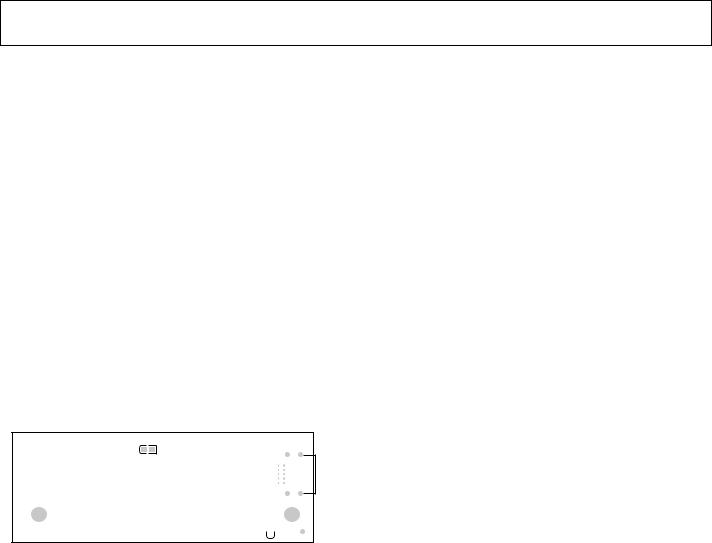
There are two LEDs located on the SDP-S board (see Figure 3).
Power LED (PWR)
The green power LED indicates that the SDP-S board is powered. This is not an indication of USB connectivity between the SDP-S and the PC.
 S–SDP
S–SDP
Rev 1.0
LED1 |
J2 |
|
|
|
|
|
|
|
|
|
|
|
|
|
|
|
|
|
|
|
|
|
|
|
|
|
|
|
|
|
|
|
|
|
|
|
|
|
|
|
|
|
|
|
|
|
|
|
|
|
|
|
|
PWR |
09916-003 |
|||
|
|
|
|||||
|
|
|
|||||
|
|
||||||
|
|
||||||
Figure 3. SDP-S Board LEDs
LED1
The orange LED is an LED used as a diagnostic tool for evaluation application developers.
CONNECTOR DETAILS
The SDP-S board contains one Hirose FX8-120P-SV1(91), 120-pin header connector. Through this connector, the peripheral communication interfaces of the USB-to-serial engine are exposed. The exposed peripherals are
•SPI
•I2C/TWI
•GPIO
Also included on the connector specification are input and output power pins, ground pins, and pins reserved for future use.
Connector Pin Assignments
Table 1 lists the connector pins and identifies the functionality assigned to each connector pin on the SDP-S board.
The pinout of this connector is consistent with other connectors across the SDP family.
Rev. A | Page 5 of 16
Loading...