


TMP01FS
REV. D
Information furnished by Analog Devices is believed to be accurate and
reliable. However, no responsibility is assumed by Analog Devices for its
use, nor for any infringements of patents or other rights of third parties that
may result from its use. No license is granted by implication or otherwise
under any patent or patent rights of Analog Devices.
a
TMP01
*
One Technology Way, P.O. Box 9106, Norwood, MA 02062-9106, U.S.A.
Tel: 781/329-4700 www.analog.com
Fax: 781/326-8703 © Analog Devices, Inc., 2002
Low Power Programmable
Temperature Controller
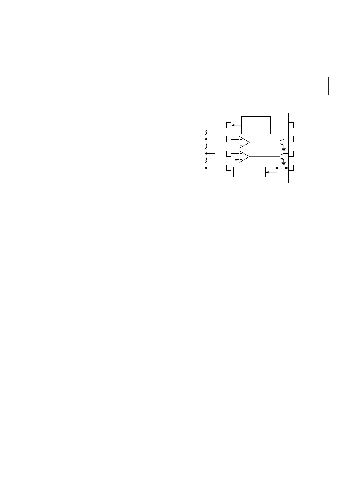
FUNCTIONAL BLOCK DIAGRAM
VPTAT
V+
TEMPERATURE
SENSOR AND
VOLTAGE
REFERENCE
2.5V
SENSOR
1
2
3
4
8
7
6
5
HYSTERESIS
GENERATOR
WINDOW
COMPARATOR
R1
TMP01
VREF
SET
HIGH
SET
LOW
GND
R2
R3
UNDER
OVER
FEATURES
–558C to +1258C (–678F to +2578F) Operation
61.08C Accuracy Over Temperature (typ)
Temperature-Proportional Voltage Output
User-Programmable Temperature Trip Points
User-Programmable Hysteresis
20 mA Open Collector Trip Point Outputs
TTL/CMOS Compatible
Single-Supply Operation (4.5 V to 13.2 V)
Low-Cost 8-Pin DIP and SO Packages
APPLICATIONS
Over/Under Temperature Sensor and Alarm
Board Level Temperature Sensing
Temperature Controllers
Electronic Thermostats
Thermal Protection
HVAC Systems
Industrial Process Control
Remote Sensors
GENERAL DESCRIPTION
The TMP01 is a temperature sensor that generates a voltage
output proportional to absolute temperature and a control signal
from one of two outputs when the device is either above or below
a specific temperature range. Both the high/low temperature trip
points and hysteresis (overshoot) band are determined by user-
selected external resistors. For high volume production, these
resistors are available on-board.
The TMP01 consists of a band gap voltage reference combined
with a pair of matched comparators. The reference provides
both a constant 2.5 V output and a voltage proportional to
absolute temperature (VPTAT) which has a precise temperature
coefficient of 5 mV/K and is 1.49 V (nominal) at 25°C. The
comparators compare VPTAT with the externally set tempera-
ture trip points and generate an open-collector output signal
when one of their respective thresholds has been exceeded.
*Protected by U.S. Patent No. 5,195,827.
Hysteresis is also programmed by the external resistor chain and
is determined by the total current drawn out of the 2.5 V refer-
ence. This current is mirrored and used to generate a hysteresis
offset voltage of the appropriate polarity after a comparator has
been tripped. The comparators are connected in parallel, which
guarantees that there is no hysteresis overlap and eliminates
erratic transitions between adjacent trip zones.
The TMP01 utilizes proprietary thin-film resistors in conjunc-
tion with production laser trimming to maintain a temperature
accuracy of ±1°C (typical) over the rated temperature range,
with excellent linearity. The open-collector outputs are capable
of sinking 20 mA, enabling the TMP01 to drive control relays
directly. Operating from a 5 V supply, quiescent current is only
500 µA (max).
The TMP01 is available in low-cost 8-pin epoxy mini-DIP and
SO (small outline) packages.

REV. D
–2–
TMP01FP, TMP01ES/TMP01FS–SPECIFICATIONS
Plastic DIP and Surface Mount
Packages (V+ = 5 V, GND = O V, –40ⴗC ≤ T
A
≤ +85ⴗC, unless otherwise noted.)
Parameter Symbol Conditions Min Typ Max Unit
INPUTS SET HIGH, SET LOW
Offset Voltage V
OS
0.25 mV
Offset Voltage Drift TCV
OS
3 µV/°C
Input Bias Current, “E” I
B
25 50 nA
Input Bias Current, “F” I
B
25 100 nA
OUTPUT VPTAT
1
Output Voltage VPTAT T
A
= 25°C, No Load 1.49 V
Scale Factor TC
VPTAT
5 mV/K
Temperature Accuracy, “E” T
A
= 25°C, No Load –1.5 ±0.5 1.5 °C
Temperature Accuracy, “F” T
A
= 25°C, No Load –3 ±1.0 3 °C
Temperature Accuracy, “E” 10°C < T
A
< 40°C, No Load ±0.75 °C
Temperature Accuracy, “F” 10°C < T
A
< 40°C, No Load ±1.5 °C
Temperature Accuracy, “E” –40°C < T
A
< 85°C, No Load –3.0 ± 1 3.0 °C
Temperature Accuracy, “F” –40°C < T
A
< 85°C, No Load –5.0 ± 2 5.0 °C
Temperature Accuracy, “E” –55°C < T
A
< 125°C, No Load ±1.5 °C
Temperature Accuracy, “F” –55°C < T
A
< 125°C, No Load ±2.5 °C
Repeatability Error
4
∆VPTAT 0.25 Degree
Long-Term Drift Error
2,6
0.25 0.5 Degree
Power Supply Rejection Ratio PSRR T
A
= 25°C, 4.5 V ≤ V+ ≤ 13.2 V ±0.02 ± 0.1 %/V
OUTPUT VREF
Output Voltage, “E” VREF T
A
= 25°C, No Load 2.495 2.500 2.505 V
Output Voltage, “F” VREF T
A
= 25°C, No Load 2.490 2.500 2.510 V
Output Voltage, “E” VREF –40°C < T
A
< 85°C, No Load 2.490 2.500 2.510 V
Output Voltage, “F” VREF –40°C < T
A
< 85°C, No Load 2.485 2.500 2.515 V
Output Voltage, “E” VREF –55°C < T
A
< 125°C, No Load 2.5 ± 0.01 V
Output Voltage, “F” VREF –55°C < T
A
< 125°C, No Load 2.5 ± 0.015 V
Drift TC
VREF
–10 ppm/°C
Line Regulation 4.5 V ≤ V+ ≤ 13.2 V ±0.01 ± 0.05 %/V
Load Regulation 10 µA ≤ I
VREF
≤ 500 µA ±0.1 ±0.25 %/mA
Output Current, Zero Hysteresis I
VREF
7 µA
Hysteresis Current Scale Factor
1
SF
HYS
5.0 µA/°C
Turn-On Settling Time To Rated Accuracy 25 µs
OPEN-COLLECTOR OUTPUTS OVER, UNDER
Output Low Voltage V
OL
I
SINK
= 1.6 mA 0.25 0.4 V
V
OL
I
SINK
= 20 mA 0.6 V
Output Leakage Current I
OH
V+ = 12 V 1 100 µA
Fall Time t
HL
See Test Load 40 ns
POWER SUPPLY
Supply Range V+ 4.5 13.2 V
Supply Current I
SY
Unloaded, +V = 5 V 400 500 µA
I
SY
Unloaded, +V = 13.2 V 450 800 µA
Power Dissipation P
DISS
+V = 5 V 2.0 2.5 mW
NOTES
1
K = °C + 273.15.
2
Guaranteed but not tested.
3
Does not consider errors caused by heating due to dissipation of output load currents.
4
Maximum deviation between 25°C readings after temperature cycling between –55 °C and +125°C.
5
Typical values indicate performance measured at T
A
= 25°C.
6
Observed in a group sample over an accelerated life test of 500 hours at 150°C.
Specifications subject to change without notice.
Test Load
20pF
1k⍀
V+

REV. D
–3–
TMP01
TMP01
TMP01FJ–SPECIFICATIONS
TO-99 Metal Can Package (V+ = 5 V, GND = O V, –40ⴗC ≤ T
A
≤ +85ⴗC,
unless otherwise noted.)
Parameter Symbol Conditions Min Typ Max Unit
INPUTS SET HIGH, SET LOW
Offset Voltage V
OS
0.25 mV
Offset Voltage Drift TCV
OS
3 µV/°C
Input Bias Current, “F” I
B
25 100 nA
OUTPUT VPTAT
1
Output Voltage VPTAT T
A
= 25°C, No Load 1.49 V
Scale Factor TC
VPTAT
5 mV/K
Temperature Accuracy, “F” T
A
= 25°C, No Load –3 ± 1.0 3 °C
10°C < T
A
< 40°C, No Load ±1.5 °C
–40°C < T
A
< 85°C, No Load –5.0 ± 2 5.0 °C
–55°C < T
A
< 125°C, No Load ±2.5 °C
Repeatability Error
4
∆VPTAT 0.25 Degree
Long-Term Drift Error
2,6
0.25 0.5 Degree
Power Supply Rejection Ratio PSRR T
A
= 25°C, 4.5 V ≤ V+ ≤ 13.2 V ±0.02 ±0.1 %/V
OUTPUT VREF
Output Voltage, “F” VREF T
A
= 25°C, No Load 2.490 2.500 2.510 V
VREF –40°C < T
A
< 85°C, No Load 2.480 2.500 2.520 V
VREF –55°C < T
A
< 125°C, No Load 2.5 ± 0.015 V
Drift TC
VREF
–10 ppm/°C
Line Regulation 4.5 V ≤ V+ ≤ 13.2 V ±0.01 ± 0.05 %/V
Load Regulation 10 µA ≤ I
VREF
≤ 500 µA ±0.1 ±0.25 %/mA
Output Current, Zero Hysteresis I
VREF
7 µA
Hysteresis Current Scale Factor
1
SF
HYS
5.0 µA/°C
Turn-On Settling Time To Rated Accuracy 25 µs
OPEN-COLLECTOR OUTPUTS OVER, UNDER
Output Low Voltage V
OL
I
SINK
= 1.6 mA 0.25 0.4 V
V
OL
I
SINK
= 20 mA 0.6 V
Output Leakage Current I
OH
V+ = 12 V 1 100 µA
Fall Time
2
t
HL
See Test Load 40 ns
POWER SUPPLY
Supply Range V+ 4.5 13.2 V
Supply Current I
SY
Unloaded, +V = 5 V 400 500 µA
I
SY
Unloaded, +V = 13.2 V 450 800 µA
Power Dissipation P
DISS
+V = 5 V 2.0 2.5 mW
NOTES
1
K = °C + 273.15.
2
Guaranteed but not tested.
3
Does not consider errors caused by heating due to dissipation of output load currents.
4
Maximum deviation between 25°C readings after temperature cycling between –55 °C and +125°C.
5
Typical values indicate performance measured at T
A
= 25°C.
6
Observed in a group sample over an accelerated life test of 500 hours at 150°C.
Specifications subject to change without notice.
REV. D
TMP01
–4–
CAUTION
ESD (electrostatic discharge) sensitive device. Electrostatic charges as high as 4000 V readily
accumulate on the human body and test equipment and can discharge without detection. Although
the TMP01 features proprietary ESD protection circuitry, permanent damage may occur on
devices subjected to high-energy electrostatic discharges. Therefore, proper ESD precautions are
recommended to avoid performance degradation or loss of functionality.
WARNING!
ESD SENSITIVE DEVICE
ABSOLUTE MAXIMUM RATINGS
1
Maximum Supply Voltage . . . . . . . . . . . . . . . . –0.3 V to +15 V
Maximum Input Voltage
(SETHIGH, SETLOW) . . . . . . . . . –0.3 V to [(V+) +0.3 V]
Maximum Output Current (VREF, VPTAT) . . . . . . . . . 2 mA
Maximum Output Current (Open-Collector Outputs) . . 50 mA
Maximum Output Voltage (Open-Collector Outputs) . . . . 15 V
Operating Temperature Range . . . . . . . . . . . –55°C to +150°C
Dice Junction Temperature . . . . . . . . . . . . . . . . . . . . . . 150°C
Storage Temperature Range . . . . . . . . . . . . – 65°C to +150°C
Lead Temperature (Soldering 60 sec) . . . . . . . . . . . . . . 300°C
NOTES
1
Stresses above those listed under Absolute Maximum Ratings may cause perma-
nent damage to the device. This is a stress rating; functional operation at or above
this specification is not implied. Exposure to the above maximum rating conditions
for extended periods may affect device reliability.
2
Digital inputs and outputs are protected, however, permanent damage may occur
on unprotected units from high energy electrostatic fields. Keep units in conduc-
tive foam or packaging at all times until ready to use. Use proper antistatic handling
procedures.
3
Remove power before inserting or removing units from their sockets.
Package Type θ
JA
θ
JC
Unit
8-Pin Plastic DIP (P) 103
1
43 °C/W
8-Lead SOIC (S) 158
2
43 °C/W
8-Lead TO-99 Can (J) 150
1
18 °C/W
NOTES
1
θ
JA
is specified for device in socket (worst-case conditions).
2
θ
JA
is specified for device mounted on PCB.
ORDERING GUIDE
Temperature Package Package
Model/Grade Range
l
Description Option
TMP01FP XIND Plastic DIP N-8
TMP01ES XIND SOIC SO-8
TMP01FS XIND SOIC SO-8
TMP01FJ
2
XIND TO-99 Can H-08A
NOTES
1
XIND = –40°C to +85°C.
2
Consult factory for availability of MIL/883 version in TO-99 can.
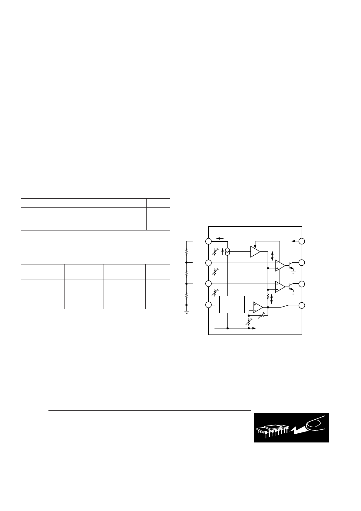
GENERAL DESCRIPTION
The TMP01 is a linear voltage-output temperature sensor,
with a window comparator that can be programmed by the user
to activate one of two open-collector outputs when a predeter-
mined temperature setpoint voltage has been exceeded. A low
drift voltage reference is available for setpoint programming.
The temperature sensor is basically a very accurate, temperature
compensated, band gap-type voltage reference with a buffered
output voltage proportional to absolute temperature (VPTAT),
accurately trimmed to a scale factor of 5 mV/K. See the Applica-
tions Information following.
The low drift 2.5 V reference output VREF is easily divided
externally with fixed resistors or potentiometers to accurately
establish the programmed heat/cool setpoints, independent of
temperature. Alternatively, the setpoint voltages can be supplied
by other ground referenced voltage sources such as user-
programmed DACs or controllers. The high and low setpoint
voltages are compared to the temperature sensor voltage, thus
creating a two-temperature thermostat function. In addition,
the total output current of the reference (I
VREF
) determines the
magnitude of the temperature hysteresis band. The open collector
outputs of the comparators can be used to control a wide variety
of devices.
VPTAT
V+
ENABLE
TMP01
VREF
SET
HIGH
SET
LOW
GND
7
8
1
2
3
4
6
HYSTERESIS
CURRENT
CURRENT
MIRROR
I
HYS
VOLTAGE
REFERENCE
AND
SENSOR
1k⍀
HYSTERESIS
VOLTAGE
5
TEMPERATURE
OUTPUT
WINDOW
COMPARATOR
UNDER
OVER
Figure 2. Detailed Block Diagram
REV. D
–5–
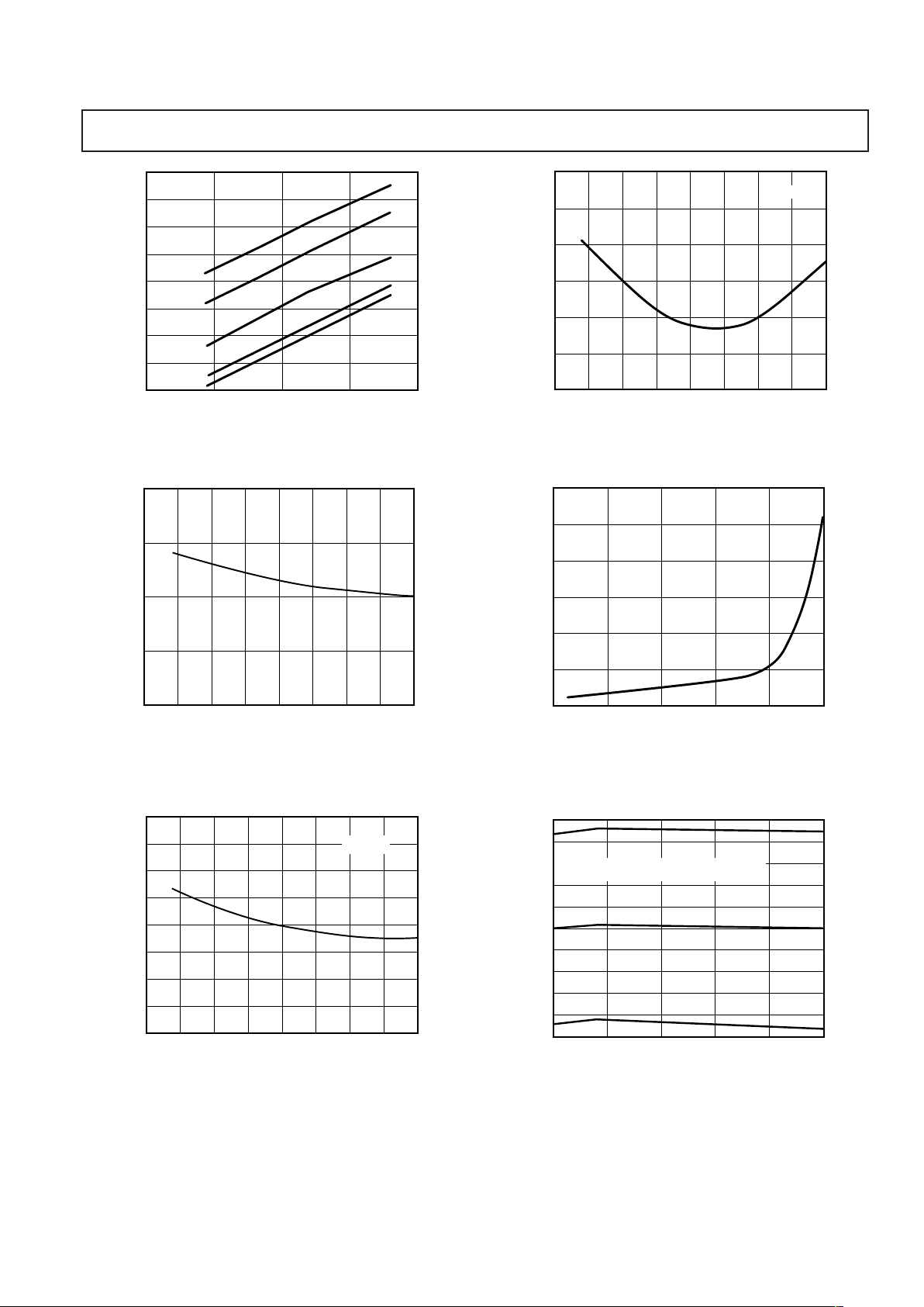
Typical Performance Characteristics–TMP01
20501510
SUPPLY VOLTAGE – V
SUPPLY CURRENT – A
550
350
400
375
450
425
475
500
525
+25ⴗC
+125ⴗC
+85ⴗC
–55ⴗC
–40ⴗC
TPC 1. Supply Current vs. Supply Voltage
5.0
3.0
4.5
3.5
4.0
–75 125–50 1007550250–25
TEMPERATURE – ⴗC
MINIMUM SUPPLY VOLTAGE – V
TPC 2. Minimum Supply Voltage vs. Temperature
–75 125–50 1007550250–25
+2.0
–3.0
+1.0
–1.0
0
+1.5
+0.5
–0.5
–1.5
TEMPERATURE – ⴗC
VPTAT ERROR – ⴗC
V+ = 5V
TPC 3. VPTAT Accuracy vs. Temperature
2.508
2.496
2.500
2.504
2.506
2.502
2.498
–75 125–50 1007550250–25
TEMPERATURE – ⴗC
VREF – V
V+ = 5V
TPC 4. VREF Accuracy vs. Temperature
6.0
0
3.0
1.0
2.0
5.0
4.0
50100403020
V
C
= 15V
V+ = 5V
T
A
= 25ⴗC
I
C
– mA
V
CE
– V
TPC 5. Open-Collector Output (
OVER
,
UNDER
) Saturation
Voltage vs. Output Current
2.510
2.490
2.496
2.492
2.494
2.502
2.498
2.500
2.504
2.506
2.508
10002000 800400 600
X + 3
X
X – 3
CURVES NOT NORMALIZED
EXTRAPOLATED FROM OPERATING LIFE DATA
T = HOURS OF OPERATION AT 125ⴗC; V+ = 5V
VREF – V
TPC 6. VREF Long Term Drift Accelerated by Burn-In
 Loading...