


 Loading...
Evaluation Board User Guide
UG-285
One Technology Way •P.O. Box 9106 •Norwood, MA 02062-9106, U.S.A. •Tel: 781.329.4700 •Fax: 781.461.3113 •www.analog.com
Evaluating the AD5544 Current Output/Serial Input DAC
FEATURES
Full-featured evaluation board for the AD5544
Graphic user interface software for board control and data analysis
Connector to EVAL-SDP-CB1Z system demonstration platform board
Various power supply options
APPLICATIONS
Automatic test equipment
Instrumentation
Digitally controlled calibration
GENERAL DESCRIPTION
The AD5544 quad, 16-bit, current output, digital-to-analog converter (DAC) is designed to operate in a 2.7 V to 5.5 V supply range. But this voltage is limited up to 3.3 V due to EVAL-SDP-CB1Z restrictions.
The applied external reference input voltage (VREFx) determines the full-scale output current. Integrated feedback resistors (RFBx) provide temperature-tracking, full-scale voltage outputs when combined with an external I-to-V precision amplifier.
A double-buffered serial data interface offers high speed, 3-wire, SPIand microcontroller-compatible inputs using serial data in (SDI), chip select (CS), and clock (CLK) signals. In addition, a serial data out pin (SDO) allows for daisy-chaining when multiple packages are used. A common, level-sensitive, load DAC strobe (LDAC) input allows the simultaneous update of all DAC outputs from previously loaded input registers. Additionally, an internal power-on reset forces the output voltage to 0 at system turn on. An MSB pin allows system reset assertion (RS) to force all registers to zero code when MSB = 0 or to half-scale code when MSB = 1.
The AD5544 is packaged in a compact 28-lead SSOP.
The EVAL-AD5544/45SDZ board is used in conjunction with the EVAL-SDP-CB1Z system demonstration platform (SDP) board available from Analog Devices, Inc., which is purchased separately from the evaluation board. The USB-to-SPI communication to the AD5544 is completed using this Blackfin®-based demonstration board. The software offers a waveform generator.
EVAL-SDP-CB1Z
GPIO 
USB
SPORT 
FUNCTIONAL BLOCK DIAGRAM
|
|
ADR01 |
|
|
|
|
|
REFERENCE |
|
|
|||
|
|
VREFx |
IOUTA |
AD8065 |
|
|
LDAC |
|
|
|
|||
|
|
I-TO-V |
VOUTA |
|||
|
|
|
|
|
||
RS |
AD5544 |
|
|
|||
MSB |
|
|
||||
|
|
|
|
|
||
|
|
|
IOUTD |
AD8065 |
|
|
|
|
|
I-TO-V |
|
||
CS |
SCLK |
SDIN |
SDO |
VOUTD |
||
|
||||||
|
|
|
|
|
09900-001 |
|
Figure 1.
PLEASE SEE THE LAST PAGE FOR AN IMPORTANT |
Rev. A | Page 1 of 12 |
WARNING AND LEGAL TERMS AND CONDITIONS. |

UG-285 |
Evaluation Board User Guide |
TABLE OF CONTENTS |
|
Features .............................................................................................. |
1 |
Applications....................................................................................... |
1 |
General Description ......................................................................... |
1 |
Functional Block Diagram .............................................................. |
1 |
Revision History ............................................................................... |
2 |
Evaluation Board Software .............................................................. |
3 |
Installing the Software ................................................................. |
3 |
REVISION HISTORY |
|
5/12—Rev. 0 to Rev. A |
|
Changes to General Description Section ...................................... |
1 |
Changes to Figure 2.......................................................................... |
3 |
Changes to Evaluation Board Schematics and Artwork Section... |
5 |
5/11—Revision 0: Initial Version |
|
Running the Software ................................................................... |
3 |
Using the Evaluation Board Software ............................................. |
4 |
Example .......................................................................................... |
4 |
Evaluation Board Schematics and Artwork................................... |
5 |
Evaluation Board Layout.............................................................. |
8 |
Related Links...................................................................................... |
9 |
Rev. A | Page 2 of 12

Evaluation Board User Guide |
UG-285 |
EVALUATION BOARD SOFTWARE
09900-002
Figure 2. Device Manager Showing the SDP Board Connected
INSTALLING THE SOFTWARE
The EVAL-AD5544/45SDZ evaluation kit includes the software and drivers on CD. To install the software, do the following:
1.Install the software before connecting the SDP board to the USB port of the PC.
2.Start the Windows® operating system and insert the EVALAD5544/45SDZ evaluation kit CD.
3.Download the EVAL-AD5544/45SDZ LabVIEW™ software. The correct driver, SDPDriversNET, for the SDP board should download automatically after LabVIEW is downloaded, supporting both 32and 64-bit systems. However, if the drivers do not download automatically, the driver executable file can also be found in the Program Files/Analog Devices folder. Follow the on-screen prompts to install it.
4.After installation of the software and drivers is complete, plug the EVAL-AD5544/45SDZ into the SDP board and the SDP board into the PC using the USB cable included in the box.
5.When the software detects the evaluation board, proceed through any dialog boxes that appear to finalize the installation (Found New Hardware Wizard/Install the Software Automatically and so on).
RUNNING THE SOFTWARE
To run the evaluation board program, do the following:
1.Click Start/All Programs/Analog Devices/EVALAD5544/45SDZ.
2.If the SDP board is not connected to the USB port when the software is launched, a connectivity error displays (see Figure 3). Simply connect the evaluation board to the USB port of the PC, wait a few seconds, click Rescan, and follow the instructions.
09900-003
Figure 3.
Rev. A | Page 3 of 12
UG-285
USING THE EVALUATION BOARD SOFTWARE
Once the software is launched, the main window pops up (see Figure 4).
09900-004
Figure 4. Main Window
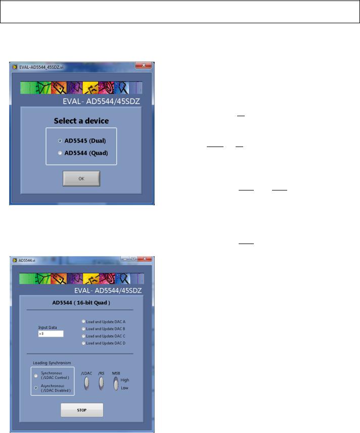
The first step is to select the device to use that is connected to the SDP board, in this case the AD5544, and click OK.
After selecting the device, the AD5544 evaluation software window appears (see Figure 5) to start writing to the device.
09900-005
Figure 5. AD5544 Evaluation Software Window
Evaluation Board User Guide
The desired 16-bit data loads and updates one of the four DACs that you selected within the AD5544 part.
There are two modes for loading the data. Synchronous mode enables you to program each channel separately and update them simultaneously. Program LDAC high, load the channels, and finally pull LDAC low. Asynch-ronous mode enables you to load and update each channel separately (the LDAC button is ignored in this case).
The reset button, RS, updates all channel outputs to zero scale or midscale when MSB is pulled low or high.
EXAMPLE
With LDAC and RS tied high for asynchronous loading mode, specify quarter scale (0x4000, 16384d) in the Input Data box and click Load and Update DAC A. The expected output obtained is
VOUT = −VREF ×65D,536 = −10×1665,,384536 = −2.5 V
When you change the loading synchronism mode to synchronous and write the value 0xC000 (49152d), you see no change in the output until LDAC is tied low. The expected output for this case is
VOUT = −VREF ×65,536D = −10×65,53649,152 = −7.5 V
Rev. A | Page 4 of 12
Loading...