


DS0026H-883
NSC DS0026H-883, DS0026H-SMD, DS0026H-MLS, DS0026H, DS0026CL Datasheet
...
DS0026
Dual High-Speed MOS Driver
General Description
DS0026 is a low cost monolithic high speed two phase MOS
clock driver and interface circuit. Unique circuit design provides both very high speed operation and the ability to drive
large capacitive loads. The device accepts standard TTL
outputs and converts them to MOS logic levels. The device
may be driven from standard 54/74 series and 54S/74S
series gates and flip-flops or from drivers such as the
DS8830 or DM7440. The DS0026 is intended for applications in which the output pulse width is logically controlled;
i.e., the output pulse width is equal to the input pulse width.
The DS0026 is designed to fulfill a wide variety of MOS
interface requirements. Information on the correct usage of
the DS0026 in these as well as other systems is included in
the application note AN-76.
Features
n Fast rise and fall times—20 ns 1000 pF load
n High output swing—20V
n High output current drive—
±
1.5 amps
n TTL compatible inputs
n High rep rate—5 to 10 MHz depending on power
dissipation
n Low power consumption in MOS “0” state—2 mW
n Drives to 0.4V of GND for RAM address drive
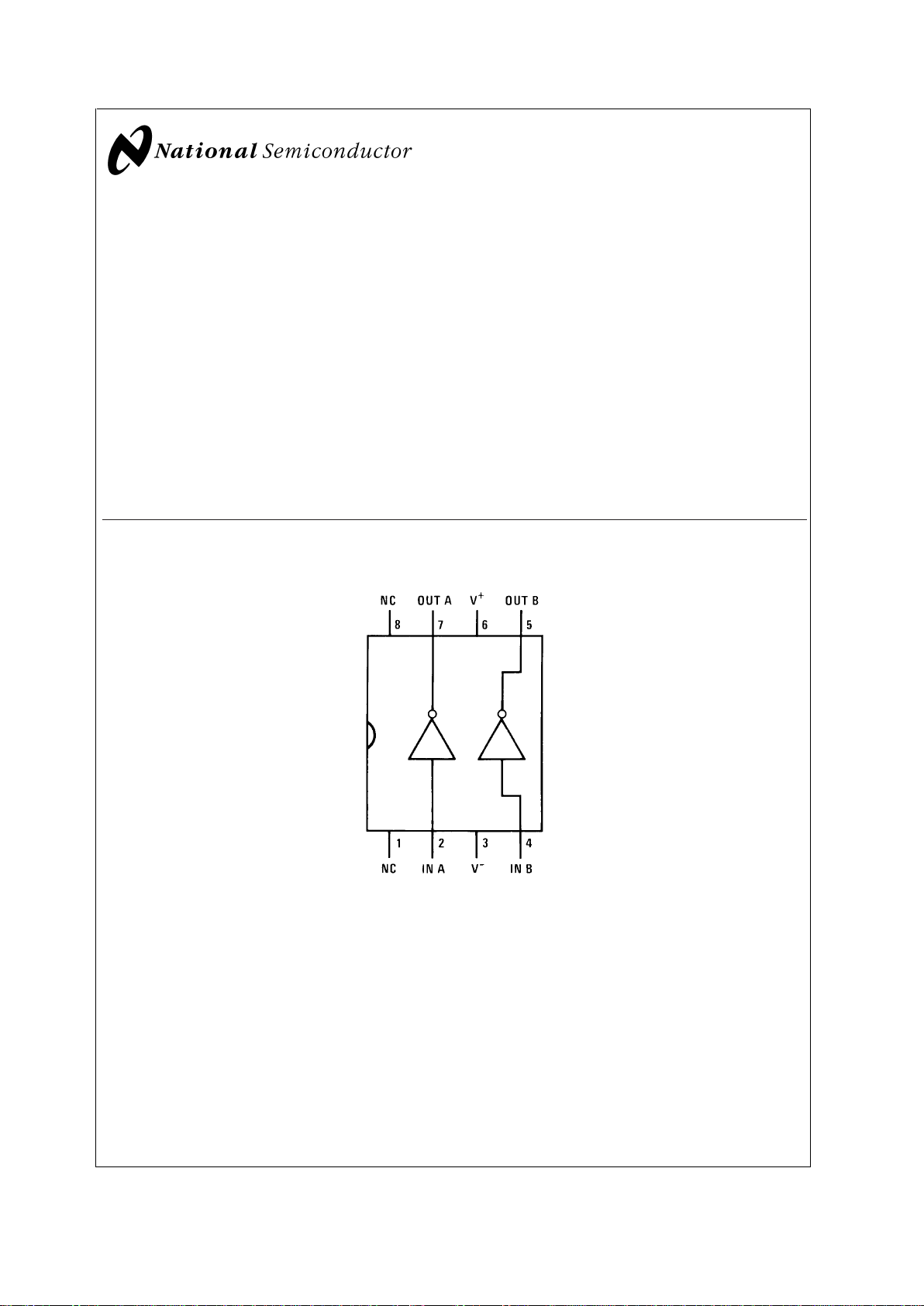
Connection Diagram (Top View)
Dual-In-Line Package
00585302
February 2002
DS0026 Dual High-Speed MOS Driver
© 2002 National Semiconductor Corporation DS005853 www.national.com

Absolute Maximum Ratings (Note 1)
If Military/Aerospace specified devices are required,
please contact the National Semiconductor Sales Office/
Distributors for availability and specifications.
(V
+
)−(V−) Differential Voltage 22V
Input Current 100 mA
Input Voltage (V
IN
)−(V−) 5.5V
Peak Output Current 1.5A
Storage Temperature Range −65˚C to +150˚C
Lead Temperature
(Soldering, 10 sec.) 300˚C
Operating Ratings
(V+)−(V−) Differential Voltage 10V to 20V
Maximum Power Dissipation at T
A
= 25˚C (Note 7) 1168mW
N08E θ
JA
107˚C/W
N08E θ
JC
37˚C/W
M08A θ
JA
180˚C/W
MUA08A θ
JA
220˚C/W
Operating Temperature Range, T
A
0˚C to +70˚C
Ordering Information
Order Number Package Type NS Package Number
DS0026CN M-DIP N08E
DS0026CMA SOIC M08A
DS0026CMM MSOP MUA08A
Electrical Characteristics (Notes 2, 3, 4)
Symbol Parameter Conditions Min Typ Max Units
V
IH
Logic “1” Input Voltage V−= 0V 2 1.5 V
I
IH
Logic “1” Input Current VIN−V−= 2.4V 10 15 mA
V
IL
Logic “0” Input Voltage V−= 0V 0.6 0.4 V
I
IL
Logic “0” Input Current VIN−V−= 0V −3 −10 µA
V
OL
Logic “1” Output Voltage VIN−V−= 2.4V, IOL= 1 mA V−+0.7 V−+1.0 V
V
OH
Logic “0” Output Voltage VIN−V−= 0.4V, VSS≥ V++ 1.0V
I
OH
=−1mA
V
+
− 1.0 V+−0.8 V
I
CC(ON)
“ON” Supply Current
(one side on)
V+−V−= 20V, VIN−V−= 2.4V
30 40 mA
I
CC(OFF)
“OFF” Supply Current V+−V−= 20V,
V
IN
−V−=0V
10 100 µA
Switching Characteristics
(TA= 25˚C) (Notes 5, 6)
Symbol Parameter Conditions Min Typ Max Units
t
ON
Turn-On Delay
(Figure 1
) 5 7.5 12 ns
(Figure 2
)11ns
t
OFF
Turn-Off Delay
(Figure 1
)1215ns
(Figure 2
)13ns
t
r
Rise Time
(Figure 1
),
(Note 5)
C
L
= 500 pF 15 18 ns
C
L
= 1000 pF 20 35 ns
(Figure 2
),
(Note 5)
C
L
= 500 pF 30 40 ns
C
L
= 1000 pF 36 50 ns
t
f
Fall Time
(Figure 1
),
(Note 5)
C
L
= 500 pF 12 16 ns
C
L
= 1000 pF 17 25 ns
(Figure 2
),
(Note 5)
C
L
= 500 pF 28 35 ns
C
L
= 1000 pF 31 40 ns
Note 1: “Absolute Maximum Ratings” are those values beyond which the safety of the device cannot be guaranteed. Except for “Operating Temperature Range”
they are not meant to imply that the devices should be operated atthese limits. The table of “Electrical Characteristics provides conditions for actual device operation.
Note 2: These specifications apply for V
+−V−
= 10V to 20V, CL= 1000 pF, over the temperature range of 0˚C to +70˚C for the DS0026CN.
Note 3: All currents into device pins shown as positive, out of device pins as negative, all voltages referenced to ground unless otherwise noted. All values shown
as max or min on absolute value basis.
DS0026
www.national.com 2
Switching Characteristics (Continued)
Note 4: All typical values for TA= 25˚C.
Note 5: Rise and fall time are given for MOS logic levels; i.e., rise time is transition from logic “0” to logic “1” which is voltage fall.
Note 6: The high current transient (as high as 1.5A) through the resistance of the internal interconnecting V
−
lead during the output transition from the high state
to the low state can appear as negative feedback to the input. If the external interconnecting lead from the driving circuit to V
−
is electrically long, or has significant
dc resistance, it can subtract from the switching response.
Note 7: Derate N08E package 9.3 mW/˚C for T
A
above 25˚C.
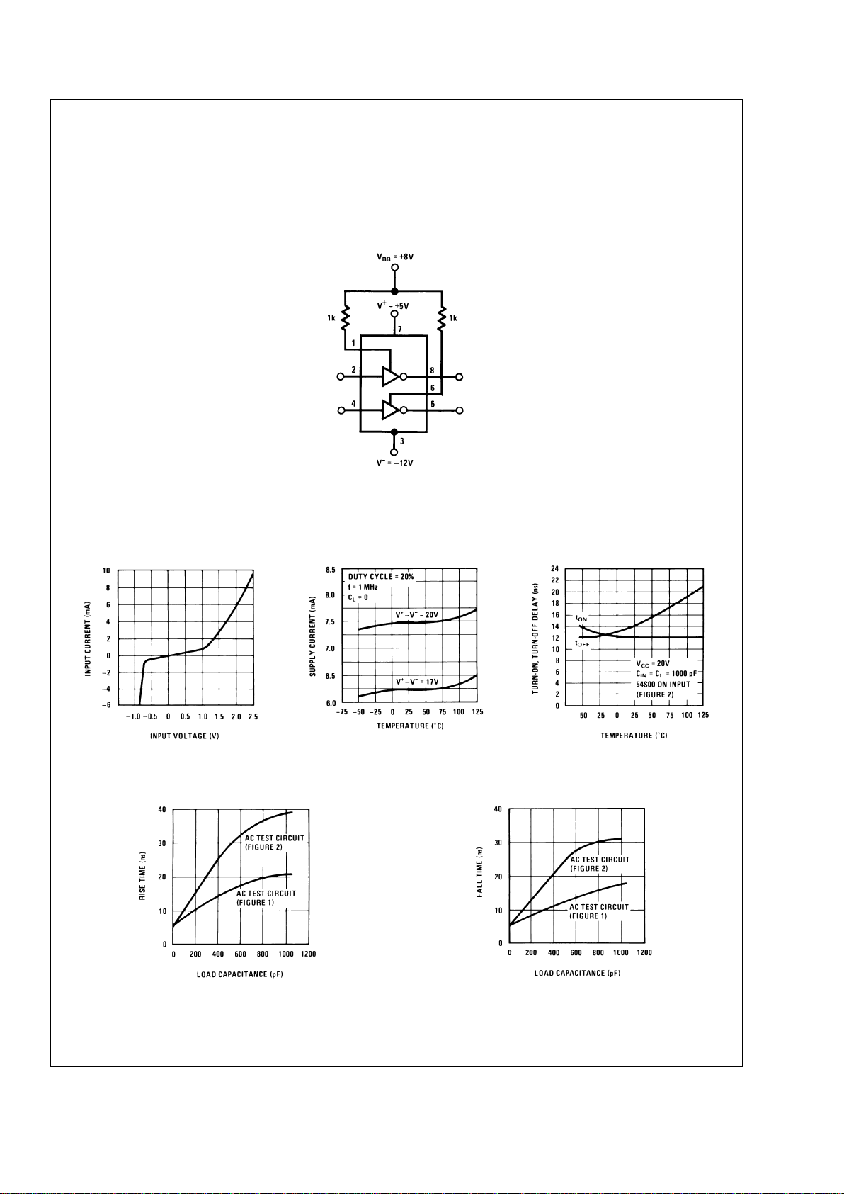
Typical VBBConnection
00585308
Typical Performance Characteristics
Input Current vs Input Voltage Supply Current vs Temperature
Turn-On and Turn-Off Delay
vs Temperature
00585322
00585323
00585324
Rise Time vs Load
Capacitance
Fall Time vs Load
Capacitance
00585325
00585326
DS0026
www.national.com3
 Loading...