


NSC CLC532MDC, CLC532AMC, CLC532AJP, CLC532AJE, 5962-9203501MCA Datasheet
...N |
June 1999 |
|
CLC532
High-Speed 2:1 Analog Multiplexer
General Description
The CLC532 is a high-speed 2:1 multiplexer with active input and output stages. The CLC532 also employs a closed-loop design which dramatically improves accuracy. This monolithicdevice is constructed using an advanced high-performance bipolar process.
The CLC532 has been specifically designed to provide settling times of 17ns to 0.01%. This, coupled with the adjustable noise-bandwidth, makes the CLC532 an ideal choice for infrared and CCD imaging systems. Channel-to-channel isolation is better than 80dB @ 10MHz. Low distortion (80dBc) and spurious signal levels make the CLC532 a very suitable choice for both I/Q processors and receivers.
TheCLC532isofferedoverboththeindustrialandmilitarytemperature ranges. The Industrial versions, CLC532AJP\AJE\AID, are specified from -40°C to +85°C and are packaged in 14-pin plastic DIP's, 14-pin SOIC'sand14-pinSide-Brazedpackages. Theextendedtemperature versions,CLC532A8B/A8D/A8L-2,arespecifiedfrom-55°Cto+125°C and are packaged in a 14-pin hermetic DIP and 20-terminal LCC packages. (Contact factory for LCC and CERDIP availability.)
Ordering Information ...
CLC532AJP |
-40oC to +85oC |
14-pin plastic DIP |
CLC532AJE |
-40oC to +85oC |
14-pin plastic SOIC |
CLC532ALC |
-40oC to +85oC |
dice |
CLC532AMC |
-55oC to +125oC |
dice, MIL-STD-833 |
CLC532A8B |
-55oC to +125oC |
14-pin CERDIP; |
|
|
MIL-STD-883 |
CLC532A8L-2A |
-55oC to +125oC |
20-terminal LCC; |
|
|
MIL-STD-883 |
Contact factory for other packages and DESC SMD number.
Features
■12-bit settling (0.01%) - 17ns
■Low noise - 32 Vrms
■High isolation - 80dB @ 10MHz
■Low distortion - 80dBc @ 5MHz
■Adjustable bandwidth - 190MHz (max)
Applications
■Infrared system multiplexing
■CCD sensor signals
■Radar I/Q switching
■High definition video HDTV
■Test and calibration
Speed-High |
CLC532 |
Multiplexer Analog 2:1 |
|
Typical Application
CHANNEL A |
|
|
CCOMP1 |
|
2 |
INA |
|
|
|
1 |
|
|
|
|
RIN |
12 |
|
|
|
|
CLC532 |
11 |
VOUT |
|
|
6 |
|
||
CHANNEL B |
10 |
RL |
||
|
||||
4 |
INB |
DREF |
|
|
3 |
|
|
||
7 |
|
|
||
RIN |
|
|
CCOMP2 |
|
CHANNEL |
SELECT OUTPUT |
|||
1 |
Channel A |
|||
SELECT |
||||
|
0 |
Channel B |
||
1999 National Semiconductor Corporation
20-Terminal LCC
|
DGND |
NC |
IN |
NC |
GND |
|
|
|
|
B |
|
|
|
|
8 |
7 |
6 |
5 |
4 |
INDEX CORNER |
|
|
|
|
|
|
|
DREF |
9 |
|
|
|
3 |
INA |
SELECT 10 |
|
|
|
2 |
GND |
|
NC 11 |
TOP VIEW |
1 |
NC |
|||
VEE |
12 |
|
|
|
20 |
+Vcc |
VEE |
13 |
|
|
|
19 |
+Vcc |
|
14 15 |
16 |
17 |
18 |
|
|
|
COMP |
NC |
OUTPUT |
NC |
COMP |
|
|
2 |
1 |
|
|||
Pinout
DIP & SOIC
|
|
|
|
|
|
|
GND |
|
1 |
|
14 |
|
+VCC |
|
|
|
||||
INA |
|
2 |
|
13 |
|
+VCC |
|
|
|||||
GND |
|
3 |
|
12 |
|
COMP1 |
|
|
|||||
INB |
|
4 |
|
11 |
|
OUTPUT |
|
|
|||||
DGND |
|
5 |
|
10 |
|
COMP2 |
|
|
|||||
|
|
|||||
DREF |
|
6 |
|
9 |
|
VEE |
|
|
|||||
|
|
|||||
SELECT |
|
7 |
|
8 |
|
VEE |
|
|
http://www.national.com
Printed in the U.S.A.

Electrical Characteristics (+VCC=+5.0V; -VEE=-5.2V; RIN=50Ω; RL=500Ω; CCOMP=10pF; ECL Mode, pin 6 = NC)
PARAMETER1 |
|
CONDITIONS |
TYP |
|
MAX/MIN RATINGS2 |
|
UNITS |
SYMBOL |
||||||
Case Temperature |
CLC532AJP/AJE/AIB |
+25° C |
|
-40° C |
+25° C |
+85° C |
|
|
|
|
|
|
||
|
|
|
|
|
|
|
|
|
|
|
|
|
||
FREQUENCY DOMAIN PERFORMANCE |
|
|
|
|
|
|
|
|
|
|
|
|
||
-3dB bandwidth |
|
VOUT<0.1Vpp |
190 |
|
140 |
140 |
110 |
|
MHz |
SSBW |
||||
-3dB bandwidth |
|
VOUT=2Vpp |
45 |
|
35 |
35 |
30 |
|
MHz |
LSBW |
||||
gain flatness |
|
VOUT<0.1Vpp |
0.2 |
|
0.7 |
0.7 |
0.8 |
|
dB |
GFP |
||||
peaking |
|
0.1MHz to 200MHz |
|
|
||||||||||
rolloff |
|
0.1MHz to 100MHz |
1.0 |
|
1.8 |
1.8 |
2.6 |
|
dB |
GFR |
||||
linear phase deviation |
dc to 100MHz |
2.0 |
|
|
|
|
|
deg |
LPD |
|||||
differential |
gain |
|
CCOMP = 5pF; RL=150Ω |
0.05 |
|
|
|
|
|
% |
|
|
|
DG |
differential |
phase |
CCOMP = 5pF; RL=150Ω |
0.01 |
|
75 |
75 |
74 |
|
deg |
DP |
||||
crosstalk rejection |
2Vpp, 10MHz |
80 |
|
|
dB |
CT10 |
||||||||
|
|
|
2Vpp, 20MHz |
74 |
|
69 |
69 |
68 |
|
dB |
CT20 |
|||
|
|
|
2Vpp, 30MHz |
68 |
|
63 |
63 |
62 |
|
dB |
CT30 |
|||
|
|
|
|
|
|
|
|
|
|
|
|
|
||
TIME DOMAIN PERFORMANCE |
|
|
|
|
|
|
|
|
|
|
|
|
||
rise and fall time |
|
0.5V step |
2.7 |
|
3.3 |
3.3 |
3.8 |
|
ns |
TRS |
||||
|
|
|
2V step |
10 |
|
12.5 |
12.5 |
14.5 |
|
ns |
TRL |
|||
settling time |
2V step; from 50% VOUT |
±0.0025% |
35 |
|
24 |
24 |
27 |
|
ns |
TS14 |
||||
|
|
|
±0.01% |
17 |
|
|
ns |
TSP |
||||||
|
|
|
±0.1% |
13 |
|
18 |
18 |
21 |
|
ns |
TSS |
|||
overshoot |
|
|
2.0V step |
2 |
|
5 |
5 |
6 |
|
% |
|
|
|
OS |
slew rate |
|
|
|
160 |
|
130 |
130 |
110 |
|
V/µs |
SR |
|||
|
|
|
|
|
|
|
|
|
|
|
|
|
||
SWITCH PERFORMANCE |
|
|
|
|
|
|
|
|
|
|
|
|
||
channel to channel switching time |
50% SELECT to 10%VOUT |
5 |
|
7 |
7 |
8 |
|
ns |
SWT10 |
|||||
(2V step at output) |
50% SELECT to 90%VOUT |
15 |
|
20 |
20 |
23 |
|
ns |
SWT90 |
|||||
switching |
transient |
|
30 |
|
|
|
|
|
mV |
ST |
||||
|
|
|
|
|
|
|
|
|
|
|
|
|||
DISTORTION AND NOISE PERFORMANCE |
|
|
|
|
|
|
|
|
|
|
|
|||
2nd harmonic distortion |
2Vpp, 5MHz |
80 |
|
67 |
67 |
67 |
|
dBc |
HD2 |
|||||
3rd harmonic distortion |
2Vpp, 5MHz |
86 |
|
68 |
68 |
68 |
|
dBc |
HD3 |
|||||
equivalent |
input |
noise |
|
|
|
|
|
|
|
|
|
|
|
|
spot noise voltage |
>1MHz |
3.1 |
|
|
|
|
|
nV/√ |
Hz |
|
SNF |
|||
integrated noise |
1MHz to 100MHz |
32 |
|
42 |
42 |
46 |
|
µVrms |
INV |
|||||
spot noise current |
|
3 |
|
|
|
|
|
pA/√ |
Hz |
|
SNC |
|||
|
|
|
|
|
|
|
|
|
|
|
|
|
||
STATIC AND DC PERFORMANCE |
|
|
|
|
|
|
|
|
|
|
|
|
||
* analog output offset voltage |
|
1 |
|
6.5 |
3.5 |
5.5 |
|
mV |
VOS |
|||||
temperature coefficient |
|
15 |
|
90 |
|
20 |
|
µV/°C |
DVIO |
|||||
analog output offset voltage matching |
|
TBD |
|
|
|
|
|
mV |
VOSM |
|||||
* analog input bias current |
|
50 |
|
250 |
120 |
120 |
|
µA |
IBN |
|||||
temperature coefficient |
|
0.3 |
|
2.0 |
|
0.8 |
|
µA/°C |
DIBN |
|||||
analog input bias current matching |
|
TBD |
|
|
|
|
|
µA |
IBNM |
|||||
analog input resistance |
|
200 |
|
90 |
120 |
120 |
|
kΩ |
RIN |
|||||
analog input capacitance |
|
2 |
|
3.0 |
2.5 |
2.5 |
|
pF |
CIN |
|||||
* gain accuracy |
|
±2V |
0.998 |
|
0.988 |
0.988 |
0.988 |
|
V/V |
GA |
||||
gain matching |
|
±2V |
TBD |
|
|
|
|
|
V/V |
GAM |
||||
integral endpoint non-linearity |
±1V (full scale) |
0.02 |
|
0.05 |
0.03 |
0.03 |
|
%FS |
ILIN |
|||||
output voltage |
|
no load |
±3.4 |
|
2.4 |
2.8 |
2.8 |
|
V |
VO |
||||
output current |
|
|
45 |
|
20 |
30 |
30 |
|
mA |
IO |
||||
output resistance |
dc |
1.5 |
|
4.0 |
2.5 |
2.5 |
|
Ω |
RO |
|||||
|
|
|
|
|
|
|
|
|
|
|
|
|
||
DIGITAL INPUT PERFORMANCE |
|
|
|
|
|
|
|
|
|
|
|
|
||
ECL mode (pin 6 floating) |
|
|
|
|
|
|
|
|
|
|
|
|
||
input voltage logic HIGH |
|
|
|
-1.1 |
-1.1 |
-1.1 |
|
V |
VIH1 |
|||||
input voltage logic LOW |
|
|
|
-1.5 |
-1.5 |
-1.5 |
|
V |
VIL1 |
|||||
input current logic HIGH |
|
14 |
|
50 |
30 |
30 |
|
µA |
IIH1 |
|||||
input current logic LOW |
|
50 |
|
270 |
110 |
110 |
|
µA |
IIL1 |
|||||
TTL mode (pin 6 = +5V) |
|
|
|
|
|
|
|
|
|
|
|
|
||
input voltage logic HIGH |
|
|
|
2.0 |
2.0 |
2.0 |
|
V |
VIH2 |
|||||
input voltage logic LOW |
|
|
|
0.8 |
0.8 |
0.8 |
|
V |
VIL2 |
|||||
input current logic HIGH |
|
14 |
|
50 |
30 |
30 |
|
µA |
IIH2 |
|||||
input current logic LOW |
|
50 |
|
270 |
110 |
110 |
|
µA |
IIL2 |
|||||
|
|
|
|
|
|
|
|
|
|
|
|
|
||
POWER REQUIREMENTS |
|
|
|
|
|
|
|
|
|
|
|
|
||
* supply current (+VCC = +5.0V) |
no load |
23 |
|
30 |
28 |
25 |
|
mA |
ICC |
|||||
* supply current (-VEE = -5.2V) |
no load |
24 |
|
31 |
30 |
26 |
|
mA |
IEE |
|||||
nominal power dissipation |
no load |
240 |
|
|
|
|
|
mW |
PD |
|||||
* power supply rejection ratio |
|
73 |
|
60 |
64 |
64 |
|
dB |
PSRR |
|||||
|
|
|
|
|
|
|
|
|
|
|
|
|
|
|
|
|
|
|
|
|
|
|
|
|
|
|
|
|
|
Min/max ratings are based on product characterization and simulation. Individual parameters are tested as noted. Outgoing quality levels are determined from tested parameters.
http://www.national.com |
2 |
Recommended Operating Conditions
positive supply voltage (+VCC) |
|
+5V |
|
negative supply voltage (-VEE) |
|
-5.2V or -5.0V |
|
differential voltage between any two GND’s |
10mV |
||
analog input voltage range |
|
|
±2V |
SELECT input voltage range (TTL mode) |
|
0.0V to +3.0V |
|
SELECT input voltage range (ECL mode) |
|
-2.0V to 0.0V |
|
CCOMP range2 |
|
|
0pF to 100pF |
thermal data |
θJC(°C/W) |
θJA(°C/W) |
|
14-pin plastic |
55 |
100 |
|
14-pin Cerdip |
35 |
85 |
|
14-pin SOIC |
35 |
105 |
|
20-terminal LCC |
35 |
50 |
|
Absolute Maximum Ratings3
positive supply voltage (+VCC) |
-0.5V to +7.0V |
|
negative supply voltage (-VEE) |
+0.5V to -7.0V |
|
differential voltage between any two GND’s |
200mV |
|
analog input voltage range |
-VEE to +VCC |
|
digital |
input voltage range |
-VEE to +VCC |
output short circuit duration (output shorted to GND) |
Infinite |
|
junction |
temperature |
+150°C |
operating temperature range |
|
|
|
CLC532AJP/AJE/AIB |
-40°C to +85°C |
storage temperature range |
-65°C to +150°C |
|
lead solder duration (+300°C) |
10 sec |
|
ESD rating |
<500V |
|
transistor count |
74 |
|
Note 1: Test levels are as follows:
*AJ : 100% tested at +25°C.
Note 2: The CLC532 does not require external CCOMP capacitors for proper operation.
Note 3: Absolute maximum ratings are limiting values, to be applied individually, and beyond which the serviceability of the circuit may be impaired. Functional operability under any of these conditions is not necessarily implied. Exposure to maximum ratings for extended periods may affect device reliability.
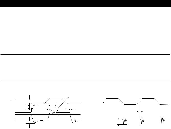
System Timing Diagram
|
|
SETTLING ERROR |
A |
|
WINDOW |
|
|
|
SELECT |
|
|
B |
|
TSx |
SWT90 |
|
|
|
|
|
SWT10 |
TRx |
TRx |
|
||
90% |
|
|
OUTPUT |
|
|
10% |
|
|
|
|
CHANNEL A = +1V |
|
OS |
CHANNEL B = -1V |
|
|
... where TSx is TS14 or TSP or TSS, and TRx is TRS ro TSL.
Switching Transient Timing Diagram
A
SELECT
B
|
|
|
|
|
|
~ |
2ns |
ST |
~ |
|
|||||
|
|
|
|
|
|
|
|
OUTPUT
Channel A = 0V
Channel B = 0V
3 |
http://www.national.com |

CLC532 Electrical Characteristics (+25°C unless specified)
http://www.national.com |
4 |
 Loading...