


May 1999
DAC0830/DAC0832
8-Bit µP Compatible, Double-Buffered D to A Converters
General Description
The DAC0830 is an advanced CMOS/Si-Cr 8-bit multiplying DAC designed to interface directly with the 8080, 8048, 8085, Z80® , and other popular microprocessors. A deposited silicon-chromium R-2R resistor ladder network divides the reference current and provides the circuit with excellent temperature tracking characteristics (0.05% of Full Scale Range maximum linearity error over temperature). The circuit uses CMOS current switches and control logic to achieve low power consumption and low output leakage current errors. Special circuitry provides TTL logic input voltage level compatibility.
Double buffering allows these DACs to output a voltage corresponding to one digital word while holding the next digital word. This permits the simultaneous updating of any number of DACs.
The DAC0830 series are the 8-bit members of a family of microprocessor-compatible DACs (MICRO-DAC™ ).
Features
nDouble-buffered, single-buffered or flow-through digital data inputs
nEasy interchange and pin-compatible with 12-bit DAC1230 series
nDirect interface to all popular microprocessors
nLinearity specified with zero and full scale adjust only Ð NOT BEST STRAIGHT LINE FIT.
nWorks with ±10V reference-full 4-quadrant multiplication
nCan be used in the voltage switching mode
nLogic inputs which meet TTL voltage level specs (1.4V logic threshold)
nOperates ªSTAND ALONEº (without µP) if desired
nAvailable in 20-pin small-outline or molded chip carrier package
Key Specifications
nCurrent settling time: 1 µs
nResolution: 8 bits
nLinearity: 8, 9, or 10 bits (guaranteed over temp.)
nGain Tempco: 0.0002% FS/ÊC
nLow power dissipation: 20 mW
nSingle power supply: 5 to 15 VDC
Typical Application
DS005608-1
BI-FET™ and MICRO-DAC™ are trademarks of National Semiconductor Corporation.
Z80® is a registered trademark of Zilog Corporation.
Converters A to D Buffered-Double Compatible, µP Bit-8 DAC0830/DAC0832
© 1999 National Semiconductor Corporation |
DS005608 |
www.national.com |

Connection Diagrams (Top Views)
Dual-In-Line and |
Molded Chip Carrier Package |
Small-Outline Packages |
|
DS005608-22
DS005608-21
www.national.com |
2 |

Absolute Maximum Ratings (Notes 1, 2)
If Military/Aerospace specified devices are required, please contact the National Semiconductor Sales Office/ Distributors for availability and specifications.
Supply Voltage (VCC) |
17 VDC |
Voltage at Any Digital Input |
VCC to GND |
Voltage at VREF Input |
±25V |
Storage Temperature Range |
−65ÊC to +150ÊC |
Package Dissipation |
|
at TA=25ÊC (Note 3) |
500 mW |
DC Voltage Applied to |
|
IOUT1 or IOUT2 (Note 4) |
−100 mV to V CC |
ESD Susceptability (Note 4) |
800V |
Lead Temperature (Soldering, 10 sec.) |
|
Dual-In-Line Package (plastic) |
260ÊC |
Dual-In-Line Package (ceramic) |
300ÊC |
Surface Mount Package |
|
Vapor Phase (60 sec.) |
215ÊC |
Infrared (15 sec.) |
220ÊC |
Operating Conditions
Temperature Range |
TMIN≤TA≤TMAX |
Part numbers with ªLCNº suffix |
0ÊC to +70ÊC |
Part numbers with ªLCWMº suffix |
0ÊC to +70ÊC |
Part numbers with ªLCVº suffix |
0ÊC to +70ÊC |
Part numbers with ªLCJº suffix |
−40ÊC to +85ÊC |
Part numbers with ªLJº suffix |
−55ÊC to +125ÊC |
Voltage at Any Digital Input |
VCC to GND |
Electrical Characteristics
VREF=10.000 VDC unless otherwise noted. Boldface limits apply over temperature, TMIN≤TA≤TMAX. For all other limits TA=25ÊC.
|
|
|
|
|
|
VCC |
= 4.75 VDC |
VCC = 5 VDC ± 5% |
|
||
|
|
|
|
|
|
VCC |
= 12 VDC ± 5% |
|
|||
|
|
|
|
|
|
VCC |
= 15.75 VDC |
|
|||
|
|
|
|
|
See |
to 15 VDC ± 5% |
Limit |
||||
Parameter |
|
Conditions |
|
|
|
||||||
|
|
|
|
|
Note |
Typ |
|
Tested |
|
Design |
Units |
|
|
|
|
|
|
|
Limit |
|
Limit |
|
|
|
|
|
|
|
|
(Note 12) |
|
|
|||
|
|
|
|
|
|
(Note 5) |
|
(Note 6) |
|
||
|
|
|
|
|
|
|
|
|
|
||
|
|
|
|
|
|
|
|
|
|
|
|
CONVERTER CHARACTERISTICS |
|
|
|
|
|
|
|
|
|||
|
|
|
|
|
|
|
|
|
|
|
|
Resolution |
|
|
|
|
8 |
|
8 |
|
8 |
bits |
|
|
|
|
|
|
|
|
|
|
|
|
|
Linearity Error Max |
|
Zero and full scale adjusted |
4, 8 |
|
|
|
|
|
|
||
|
|
|
−10V ≤VREF≤+10V |
|
|
|
|
|
|
|
|
DAC0830LJ & LCJ |
|
|
|
|
|
|
0.05 |
|
0.05 |
% FSR |
|
DAC0832LJ & LCJ |
|
|
|
|
|
|
0.2 |
|
0.2 |
% FSR |
|
DAC0830LCN, LCWM & |
|
|
|
|
|
0.05 |
|
0.05 |
% FSR |
||
LCV |
|
|
|
|
|
|
|
|
|
|
|
DAC0831LCN |
|
|
|
|
|
|
0.1 |
|
0.1 |
% FSR |
|
DAC0832LCN, LCWM & |
|
|
|
|
|
0.2 |
|
0.2 |
% FSR |
||
LCV |
|
|
|
|
|
|
|
|
|
|
|
|
|
|
|
|
|
|
|
|
|
||
Differential Nonlinearity |
Zero and full scale adjusted |
4, 8 |
|
|
|
|
|
|
|||
Max |
|
−10V ≤VREF≤+10V |
|
|
|
|
|
|
|
|
|
DAC0830LJ & LCJ |
|
|
|
|
|
|
0.1 |
|
0.1 |
% FSR |
|
DAC0832LJ & LCJ |
|
|
|
|
|
|
0.4 |
|
0.4 |
% FSR |
|
DAC0830LCN, LCWM & |
|
|
|
|
|
0.1 |
|
0.1 |
% FSR |
||
LCV |
|
|
|
|
|
|
|
|
|
|
|
DAC0831LCN |
|
|
|
|
|
|
0.2 |
|
0.2 |
% FSR |
|
DAC0832LCN, LCWM & |
|
|
|
|
|
0.4 |
|
0.4 |
% FSR |
||
LCV |
|
|
|
|
|
|
|
|
|
|
|
|
|
|
|
|
|
|
|
|
|
|
|
Monotonicity |
|
−10V ≤VREF |
LJ & LCJ |
4 |
|
|
8 |
|
8 |
bits |
|
|
|
|
≤+10V |
LCN, LCWM & LCV |
|
|
|
8 |
|
8 |
bits |
|
|
|
|
|
|
|
|
|
|
|
|
Gain Error Max |
|
Using Internal Rfb |
|
7 |
±0.2 |
|
±1 |
|
± 1 |
% FS |
|
|
|
|
−10V ≤VREF≤+10V |
|
|
|
|
|
|
|
|
Gain Error Tempco Max |
Using internal Rfb |
|
|
0.0002 |
|
|
|
0.0006 |
% |
||
|
|
|
|
|
|
|
|
|
|
|
FS/ÊC |
|
|
|
|
|
|
|
|
|
|
||
Power Supply Rejection |
All digital inputs latched high |
|
|
|
|
|
|
|
|||
|
|
|
VCC=14.5V to 15.5V |
|
0.0002 |
|
0.0025 |
|
|
% |
|
|
|
|
11.5V to 12.5V |
|
0.0006 |
|
|
|
|
FSR/V |
|
|
|
|
4.5V to 5.5V |
|
|
0.013 |
|
0.015 |
|
|
|
|
|
|
|
|
|
|
|
|
|
|
|
Reference |
|
Max |
|
|
|
15 |
|
20 |
|
20 |
kΩ |
|
|
|
|
|
|
|
|
|
|
|
|
Input |
|
Min |
|
|
|
15 |
|
10 |
|
10 |
kΩ |
|
|
|
|
|
|
|
|
|
|
||
Output Feedthrough Error |
VREF=20 Vp-p, f=100 kHz |
|
3 |
|
|
|
|
mVp-p |
|||
|
|
|
All data inputs latched low |
|
|
|
|
|
|||
|
|
|
|
|
|
|
|
|
|
||
3 |
www.national.com |

Electrical Characteristics (Continued)
VREF=10.000 VDC unless otherwise noted. Boldface limits apply over temperature, TMIN≤TA≤TMAX. For all other limits TA=25ÊC.
|
|
|
|
|
|
|
VCC |
= 4.75 VDC |
VCC = 5 VDC ± 5% |
|
||
|
|
|
|
|
|
|
VCC |
= 12 VDC ± 5% |
|
|||
|
|
|
|
|
|
|
VCC |
= 15.75 VDC |
|
|||
|
|
|
|
|
|
See |
to 15 VDC ± 5% |
Limit |
||||
Parameter |
|
Conditions |
|
|
|
|||||||
|
|
|
|
|
|
Note |
Typ |
|
Tested |
|
Design |
Units |
|
|
|
|
|
|
|
|
Limit |
|
Limit |
|
|
|
|
|
|
|
|
|
(Note 12) |
|
|
|||
|
|
|
|
|
|
|
(Note 5) |
|
(Note 6) |
|
||
|
|
|
|
|
|
|
|
|
|
|
||
|
|
|
|
|
|
|
|
|
|
|
|
|
CONVERTER CHARACTERISTICS |
|
|
|
|
|
|
|
|
|
|||
|
|
|
|
|
|
|
|
|
|
|
|
|
Output Leakage |
|
IOUT1 |
All data inputs |
LJ & LCJ |
10 |
|
|
100 |
|
100 |
nA |
|
Current Max |
|
|
latched low |
LCN, LCWM & LCV |
|
|
|
50 |
|
100 |
|
|
|
|
|
|
|
|
|
|
|||||
|
|
|
|
|
|
|
|
|
|
|
|
|
|
|
IOUT2 |
All data inputs |
LJ & LCJ |
|
|
|
100 |
|
100 |
nA |
|
|
|
|
latched high |
LCN, LCWM & LCV |
|
|
|
50 |
|
100 |
|
|
|
|
|
|
|
|
|
|
|
|
|
|
|
Output |
|
IOUT1 |
All data inputs |
|
|
|
45 |
|
|
|
|
pF |
Capacitance |
|
IOUT2 |
latched low |
|
|
|
115 |
|
|
|
|
|
|
|
IOUT1 |
All data inputs |
|
|
|
130 |
|
|
|
|
pF |
|
|
IOUT2 |
latched high |
|
|
|
30 |
|
|
|
|
|
DIGITAL AND DC CHARACTERISTICS |
|
|
|
|
|
|
|
|
|
|||
|
|
|
|
|
|
|
|
|
|
|
|
|
Digital Input |
|
Max |
Logic Low |
LJ: |
4.75V |
|
|
|
0.6 |
|
|
|
Voltages |
|
|
|
LJ: |
15.75V |
|
|
|
0.8 |
|
|
|
|
|
|
|
LCJ: |
4.75V |
|
|
|
0.7 |
|
|
VDC |
|
|
|
|
LCJ: |
15.75V |
|
|
|
0.8 |
|
|
|
|
|
|
|
LCN, LCWM, LCV |
|
|
|
0.95 |
|
0.8 |
|
|
|
|
|
|
|
|
|
|
|
|
|
|
|
|
|
Min |
Logic High |
LJ & LCJ |
|
|
|
2.0 |
|
2.0 |
VDC |
|
|
|
|
|
LCN, LCWM, LCV |
|
|
|
1.9 |
|
2.0 |
|
|
|
|
|
|
|
|
|
|
|
|
|
|
|
Digital Input |
|
Max |
Digital inputs <0.8V |
|
|
|
|
|
|
|
|
|
Currents |
|
|
|
LJ & LCJ |
|
−50 |
|
−200 |
|
−200 |
µA |
|
|
|
|
|
LCN, LCWM, LCV |
|
|
|
−160 |
|
−200 |
µA |
|
|
|
|
|
|
|
|
|
|
|
|
|
|
|
|
|
Digital inputs>2.0V |
|
|
|
|
|
|
|
|
|
|
|
|
|
LJ & LCJ |
|
0.1 |
|
+10 |
|
+10 |
µA |
|
|
|
|
|
LCN, LCWM, LCV |
|
|
|
+8 |
|
+10 |
|
|
|
|
|
|
|
|
|
|
|
|
|
|
|
Supply Current |
|
Max |
|
LJ & LCJ |
|
1.2 |
|
3.5 |
|
3.5 |
mA |
|
Drain |
|
|
|
LCN, LCWM, LCV |
|
|
|
1.7 |
|
2.0 |
|
|
|
|
|
|
|
|
|
|
|
|
|
|
|
Electrical Characteristics
VREF=10.000 VDC unless otherwise noted. Boldface limits apply over temperature, TMIN≤TA≤TMAX. For all other limits TA=25ÊC.
|
|
|
|
VCC=15.75 VDC |
VCC=12 VDC± 5% |
VCC=4.75 VDC |
VCC=5 |
|
||
|
|
|
|
to 15 VDC ± 5% |
VDC± 5% |
|
||||
|
|
|
See |
|
|
|
|
Limit |
||
Symbol |
Parameter |
Conditions |
Note |
Typ |
Tested |
Design Limit |
Typ |
Tested |
Design |
Units |
|
|
|
Limit |
Limit |
Limit |
|||||
|
|
|
|
(Note 12) |
(Note 6) |
(Note 12) |
|
|||
|
|
|
|
(Note 5) |
(Note 5) |
(Note 6) |
|
|||
|
|
|
|
|
|
|
|
|||
|
|
|
|
|
|
|
|
|
|
|
AC CHARACTERISTICS |
|
|
|
|
|
|
|
|
|
|
|
|
|
|
|
|
|
|
|
|
|
ts |
Current Setting |
VIL=0V, VIH=5V |
|
1.0 |
|
|
1.0 |
|
|
µs |
|
Time |
|
|
|
|
|
|
|
|
|
|
|
|
|
|
|
|
|
|
|
|
tW |
Write and XFER |
VIL=0V, VIH=5V |
11 |
100 |
250 |
|
375 |
600 |
|
|
|
Pulse Width Min |
|
9 |
|
320 |
320 |
|
900 |
900 |
|
|
|
|
|
|
|
|
|
|
|
|
tDS |
Data Setup Time |
VIL=0V, VIH=5V |
9 |
100 |
250 |
|
375 |
600 |
|
|
|
Min |
|
|
|
320 |
320 |
|
900 |
900 |
|
|
|
|
|
|
|
|
|
|
|
|
tDH |
Data Hold Time |
VIL=0V, VIH=5V |
9 |
|
30 |
|
|
50 |
|
ns |
|
Min |
|
|
|
30 |
|
|
50 |
|
|
|
|
|
|
|
|
|
|
|
|
|
tCS |
Control Setup Time |
VIL=0V, VIH=5V |
9 |
110 |
250 |
|
600 |
900 |
|
|
|
Min |
|
|
|
320 |
320 |
|
1100 |
1100 |
|
|
|
|
|
|
|
|
|
|
|
|
tCH |
Control Hold Time |
VIL=0V, VIH=5V |
9 |
0 |
0 |
10 |
0 |
0 |
|
|
|
Min |
|
|
|
0 |
|
|
0 |
|
|
|
|
|
|
|
|
|
|
|
|
|
Note 1: Absolute Maximum Ratings indicate limits beyond which damage to the device may occur. DC and AC electrical specifications do not apply when operating the device beyond its specified operating conditions.
Note 2: All voltages are measured with respect to GND, unless otherwise specified.
www.national.com |
4 |
Electrical Characteristics (Continued)
Note 3: The maximum power dissipation must be derated at elevated temperatures and is dictated by TJMAX, θJA, and the ambient temperature, TA. The maximum allowable power dissipation at any temperature is PD = (TJMAX − T A)/θJA or the number given in the Absolute Maximum Ratings, whichever is lower. For this device, TJMAX = 125ÊC (plastic) or 150ÊC (ceramic), and the typical junction-to-ambient thermal resistance of the J package when board mounted is 80ÊC/W. For the N pa ckage, this number increases to 100ÊC/W and for the V package this number is 120ÊC/W.
Note 4: For current switching applications, both IOUT1 and IOUT2 must go to ground or the ªVirtual Groundº of an operational amplifier. The linearity error is degraded by approximately VOS ÷ VREF. For example, if VREF = 10V then a 1 mV offset, VOS, on IOUT1 or IOUT2 will introduce an additional 0.01% linearity error.
Note 5: Tested limits are guaranteed to National's AOQL (Average Outgoing Quality Level).
Note 6: Guaranteed, but not 100% production tested. These limits are not used to calculate outgoing quality levels.
Note 7: Guaranteed at VREF=±10 VDC and VREF=±1 VDC.
Note 8: The unit ªFSRº stands for ªFull Scale Range.º ªLinearity Errorº and ªPower Supply Rejectionº specs are based on this unit to eliminate dependence onar-a p ticular VREF value and to indicate the true performance of the part. The ªLinearity Errorº specification of the DAC0830 is ª0.%05of FSR (MAX)º. This guarantees that after performing a zero and full scale adjustment (see Sections 2.5 and 2.6), the plot of the 256 analog voltage outputs will each be within 0.05%xVREF of a straight line which passes through zero and full scale.
Note 9: Boldface tested limits apply to the LJ and LCJ suffix parts only.
Note 10: A 100nA leakage current with Rfb=20k and VREF=10V corresponds to a zero error of (100x10−9 x20x103)x100/10 which is 0.02% of FS.
Note 11: The entire write pulse must occur within the valid data interval for the specified tW, tDS, tDH, and tS to apply.
Note 12: Typicals are at 25ÊC and represent most likely parametric norm.
Note 13: Human body model, 100 pF discharged through a 1.5 kΩ resistor.
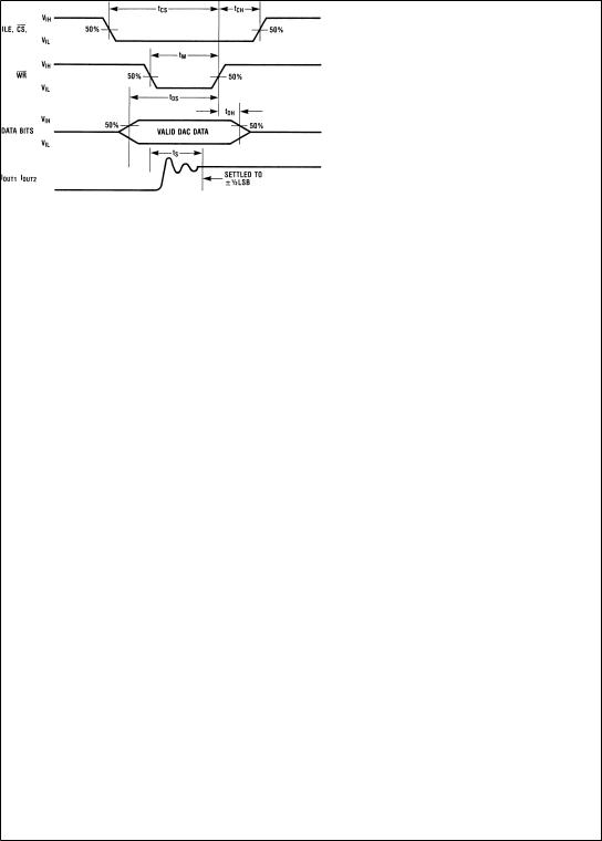
Switching Waveform
DS005608-2
5 |
www.national.com |

Definition of Package Pinouts
Control Signals (All control signals level actuated)
CS: Chip Select (active low). The CS in combination with ILE will enable WR1.
ILE: |
Input Latch Enable (active high). The ILE in combi- |
||||
|
|
|
nation with CS enables WR1. |
||
|
WR |
1: |
Write 1. The active low |
WR |
1 is used to load the digi- |
|
|
|
tal input data bits (DI) into the input latch. The data |
||
|
|
|
in the input latch is latched when WR1 is high. To |
||
|
|
|
update the input latch±CS and WR1 must be low |
||
|
|
|
while ILE is high. |
||
|
|
2: |
Write 2 (active low). This signal, in combination with |
||
WR |
|||||
|
|
|
XFER, causes the 8-bit data which is available in |
||
|
|
|
the input latch to transfer to the DAC register. |
||
XFER: Transfer control signal (active low). The XFER will enable WR2.
Other Pin Functions
DI0-DI7: Digital Inputs. DI0 is the least significant bit (LSB) and DI7 is the most significant bit (MSB).
IOUT1: DAC Current Output 1. IOUT1 is a maximum for a digital code of all 1's in the DAC register, and is
zero for all 0's in DAC register.
IOUT2: DAC Current Output 2. IOUT2 is a constant minus IOUT1 , or IOUT1 + IOUT2 = constant (I full scale for a fixed reference voltage).
Rfb: Feedback Resistor. The feedback resistor is pro-
Linearity Error
vided on the IC chip for use as the shunt feedback resistor for the external op amp which is used to provide an output voltage for the DAC. This onchip resistor should always be used (not an external resistor) since it matches the resistors which are used in the on-chip R-2R ladder and tracks these resistors over temperature.
VREF: Reference Voltage Input. This input connects an external precision voltage source to the internal R-2R ladder. VREF can be selected over the range of +10 to −10V. This is also the analog voltage input for a 4-quadrant multiplying DAC application.
VCC: Digital Supply Voltage. This is the power supply pin for the part. VCC can be from +5 to +15VDC. Operation is optimum for +15VDC
GND: The pin 10 voltage must be at the same ground
potential as IOUT1 and IOUT2 for current switching applications. Any difference of potential (VOS pin
10) will result in a linearity change of
For example, if VREF = 10V and pin 10 is 9mV offset from IOUT1 and IOUT2 the linearity change will be 0.03%.
Pin 3 can be offset ±100mV with no linearity change, but the logic input threshold will shift.
DS005608-23 |
DS005608-24 |
|
a) End point test after |
b) Best straight line |
DS005608-25 |
zero and fs adj. |
|
c) Shifting fs adj. to pass |
|
|
|
|
|
best straight line test |
Definition of Terms
Resolution: Resolution is directly related to the number of switches or bits within the DAC. For example, the DAC0830 has 28 or 256 steps and therefore has 8-bit resolution.
Linearity Error: Linearity Error is the maximum deviation from a straight line passing through the endpoints of the DAC transfer characteristic. It is measured after adjusting for zero and full-scale. Linearity error is a parameter intrinsic to the device and cannot be externally adjusted.
National's linearity ªend point testº (a) and the ªbest straight lineº test (b,c) used by other suppliers are illustrated above. The ªend point test'' greatly simplifies the adjustment procedure by eliminating the need for multiple iterations of checking the linearity and then adjusting full scale until the linearity
is met. The ªend point test'' guarantees that linearity is met after a single full scale adjust. (One adjustment vs. multiple
iterations of the adjustment.) The ªend point test'' uses a standard zero and F.S. adjustment procedure and is a much more stringent test for DAC linearity.
Power Supply Sensitivity: Power supply sensitivity is a measure of the effect of power supply changes on the DAC full-scale output.
Settling Time: Settling time is the time required from a code transition until the DAC output reaches within ±1¤2LSB of the final output value. Full-scale settling time requires a zero to full-scale or full-scale to zero output change.
Full Scale Error: Full scale error is a measure of the output error between an ideal DAC and the actual device output. Ideally, for the DAC0830 series, full scale is VREF −1LSB.
For VREF = 10V and unipolar operation, VFULL-SCALE = 10,0000V±39mV 9.961V. Full-scale error is adjustable to
zero.
www.national.com |
6 |

Definition of Terms (Continued)
Differential Nonlinearity: The difference between any two consecutive codes in the transfer curve from the theoretical 1 LSB to differential nonlinearity.
Monotonic: If the output of a DAC increases for increasing digital input code, then the DAC is monotonic. An 8-bit DAC which is monotonic to 8 bits simply means that increasing digital input codes will produce an increasing analog output.
DS005608-4
FIGURE 1. DAC0830 Functional Diagram
Typical Performance Characteristics
Digital Input Threshold |
Digital Input Threshold |
Gain and Linearity Error |
vs. Temperature |
vs. VCC |
Variation vs. Temperature |
DS005608-26 |
DS005608-27 |
DS005608-28 |
7 |
www.national.com |

Typical Performance Characteristics (Continued)
Gain and Linearity Error |
Write Pulse Width |
Data Hold Time |
Variation vs. Supply Voltage |
|
|
DS005608-29
DAC0830 Series Application Hints
These DAC's are the industry's first microprocessor compatible, double-buffered 8-bit multiplying D to A converters. Double-buffering allows the utmost application flexibility from a digital control point of view. This 20-pin device is also pin for pin compatible (with one exception) with the DAC1230, a 12-bit MICRO-DAC. In the event that a system's analog output resolution and accuracy must be upgraded, substituting the DAC1230 can be easily accomplished. By tying address bit A0 to the ILE pin, a two-byte µP write instruction (double precision) which automatically increments the address for the second byte write (starting with A0=ª1º) can be used. This allows either an 8-bit or the 12-bit part to be used with no hardware or software changes. For the simplest 8-bit application, this pin should be tied to VCC (also see other uses in section 1.1).
Analog signal control versatility is provided by a precision R-2R ladder network which allows full 4-quadrant multiplication of a wide range bipolar reference voltage by an applied digital word.
1.0 DIGITAL CONSIDERATIONS
A most unique characteristic of these DAC's is that the 8-bit digital input byte is double-buffered. This means that the data must transfer through two independently controlled 8-bit latching registers before being applied to the R-2R ladder network to change the analog output. The addition of a second register allows two useful control features. First, any DAC in a system can simultaneously hold the current DAC data in one register (DAC register) and the next data word in the second register (input register) to allow fast updating of the DAC output on demand. Second, and probably more important, double-buffering allows any number of DAC's in a system to be updated to their new analog output levels simultaneously via a common strobe signal.
DS005608-30 |
DS005608-31 |
The timing requirements and logic level convention of the register control signals have been designed to minimize or eliminate external interfacing logic when applied to most popular microprocessors and development systems. It is easy to think of these converters as 8-bit ªwrite-onlyº memory locations that provide an analog output quantity. All inputs to these DAC's meet TTL voltage level specs and can also be driven directly with high voltage CMOS logic in non-microprocessor based systems. To prevent damage to the chip from static discharge, all unused digital inputs should be tied to VCC or ground. If any of the digital inputs are inadvertantly left floating, the DAC interprets the pin as a logic ª1º.
1.1 Double-Buffered Operation
Updating the analog output of these DAC's in a double-buffered manner is basically a two step or double write operation. In a microprocessor system two unique system addresses must be decoded, one for the input latch controlled by the CS pin and a second for the DAC latch which is controlled by the XFER line. If more than one DAC is being driven, Figure 2, the CS line of each DAC would typically be decoded individually, but all of the converters could share a common XFER address to allow simultaneous updating of any number of DAC's. The timing for this operation is shown,
Figure 3.
It is important to note that the analog outputs that will change after a simultaneous transfer are those from the DAC's whose input register had been modified prior to the XFER command.
www.national.com |
8 |
 Loading...