


COP8SGE740N8
NSC COP8SGE740N8, COP8SGE728N8, COP8SGR7VEJ8, COP8SGR744V8, COP8SGR744J3 Datasheet
...
COP8SG Family
8-Bit CMOS ROM Based and OTP Microcontrollers with
8k to 32k Memory, Two Comparators and USART
General Description
The COP8SGx5 Family ROM based microcontrollers are
highly integrated COP8
™
Feature core devices with 8k to
32k memory and advanced features including Analog com-
parators, and zero external components. These single-chip
CMOS devices are suited for more complex applications re-
quiring a fullfeatured controller with larger memory, low EMI,
two comparators, and a full-duplex USART. COP8SGx7 de-
vices are 100
%
form-fit-function compatible 8k or 32k OTP
(One Time Programmable) versions for use in production or
development.
Erasable windowed versions are available for use with a
range of COP8 software and hardware development tools.
Family features include an 8-bit memory mapped architec-
ture, 15 MHz CKI with 0.67 µs instruction cycle, 14 inter-
rupts, three multi-function 16-bit timer/counters with PWM,
full duplex USART, MICROWIRE/PLUS
™
, two analog com-
parators, two power saving HALT/IDLE modes, MIWU, idle
timer, on-chip R/C oscillator, high current outputs, user se-
lectable options (WATCHDOG
™
, 4 clock/oscillator modes,
power-on-reset), 2.7V to 5.5V operation, program code se-
curity, and 28/40/44 pin packages.
Devices included in this datasheet are:
Device Memory (bytes)
RAM
(bytes)
I/O Pins Packages Temperature
COP8SGE5 8k ROM 256 24/36/40 28 DIP/SOIC, 40 DIP, 44 PLCC/QFP
-40 to +85˚C,
-40 to +125˚C
COP8SGG5 16k ROM 512 24/36/40 28 DIP/SOIC, 40 DIP, 44 PLCC/QFP
-40 to +85˚C,
-40 to +125˚C
COP8SGH5 20k ROM 512 24/36/40 28 DIP/SOIC, 40 DIP, 44 PLCC/QFP
-40 to +85˚C,
-40 to +125˚C
COP8SGK5 24k ROM 512 24/36/40 28 DIP/SOIC, 40 DIP, 44 PLCC/QFP
-40 to +85˚C,
-40 to +125˚C
COP8SGR5 32k ROM 512 24/36/40 28 DIP/SOIC, 40 DIP, 44 PLCC/QFP
-40 to +85˚C,
-40 to +125˚C
COP8SGE7 8k OTP EPROM 256 24/36/40 28 DIP/SOIC, 40 DIP, 44 PLCC/QFP
-40 to +85˚C,
-40 to +125˚C
COP8SGR7 32k OTP EPROM 512 24/36/40 28 DIP/SOIC, 40 DIP, 44 PLCC/QFP
-40 to +85˚C,
-40 to +125˚C
COP8SGR7-Q3 32k EPROM 512 24/36/40 28 DIP/SOIC, 40 DIP, 44 PLCC/QFP Room Temp.
Key Features
n Low cost 8-bit microcontroller
n Quiet Design (low radiated emissions)
n Multi-Input Wakeup pins with optional interrupts (8 pins)
n Mask selectable clock options
— Crystal oscillator
— Crystal oscillator option with on-chip bias resistor
— External oscillator
— Internal R/C oscillator
n Internal Power-On-Reset — user selectable
n WATCHDOG and Clock Monitor Logic — user selectable
n Eight high current outputs
n 256 or 512 bytes on-board RAM
n 8k to 32k ROM or OTP EPROM with security feature
CPU Features
n Versatile easy to use instruction set
n 0.67 µs instruction cycle time
n Fourteen multi-source vectored interrupts servicing
— External interrupt / Timers T0 — T3
— MICROWIRE/PLUS Serial Interface
— Multi-Input Wake Up
— Software Trap
— USART (2; 1 receive and 1 transmit)
— Default VIS (default interrupt)
n 8-bit Stack Pointer SP (stack in RAM)
n Two 8-bit Register Indirect Data Memory Pointers
n True bit manipulation
n BCD arithmetic instructions
COP8
™
, MICROWIRE/PLUS
™
, and WATCHDOG
™
are trademarks of National Semiconductor Corporation.
TRI-STATE
®
is a registered trademark of National Semiconductor Corporation.
iceMASTER
®
is a registered trademark of MetaLink Corporation.
January 2000
COP8SG Family, 8-Bit CMOS ROM Based and OTP Microcontrollers with 8k to 32k Memory, Two
Comparators and USART
© 2000 National Semiconductor Corporation DS101317 www.national.com
CPU Features (Continued)
Peripheral Features
n Multi-Input Wakeup Logic
n Three 16-bit timers (T1 — T3), each with two 16-bit
registers supporting:
— Processor Independent PWM mode
— External Event Counter mode
— Input Capture mode
n Idle Timer (T0)
n MICROWIRE/PLUS Serial Interface (SPI Compatible)
n Full Duplex USART
n Two Analog Comparators
I/O Features
n Software selectable I/O options (TRI-STATE
®
Output,Push-Pull Output, Weak Pull-Up Input, and High
Impedance Input)
n Schmitt trigger inputs on ports G and L
n Eight high current outputs
n Packages: 28 SO with 24 I/O pins, 40 DIP with 36 I/O
pins, 44 PLCC and PQFP with 40 I/O pins
Fully Static CMOS Design
n Low current drain (typically
<
4 µA)
n Two power saving modes: HALT and IDLE
Temperature Range
n −40˚C to +85˚C, −40˚C to +125˚C
Development Support
n Windowed packages for DIP and PLCC
n Real time emulation and full program debug offered by
MetaLink Development System
Block Diagram
DS101317-44
FIGURE 1. COP8SGx Block Diagram
COP8SG Family
www.national.com 2

1.0 Device Description
1.1 ARCHITECTURE
The COP8 family is based on a modified Harvard architec-
ture, which allows data tables to be accessed directly from
program memory. This is very important with modern
microcontroller-based applications, since program memory
is usually ROM or EPROM, while data memory is usually
RAM. Consequently data tables need to be contained in
non-volatile memory, so they are not lost when the microcon-
troller is powered down. In a modified Harvard architecture,
instruction fetch and memory data transfers can be over-
lapped with a two stage pipeline, which allows the next in-
struction to be fetched from program memory while the cur-
rent instruction is being executed using data memory.This is
not possible with a Von Neumann single-address bus archi-
tecture.
The COP8 family supports a software stack scheme that al-
lows the user to incorporate many subroutine calls. This ca-
pability is important when using High Level Languages. With
a hardware stack, the user is limited to a small fixed number
of stack levels.
1.2 INSTRUCTION SET
In today’s 8-bit microcontroller application arena cost/
performance, flexibility and time to market are several of the
key issues that system designers face in attempting to build
well-engineered products that compete in the marketplace.
Many of these issues can be addressed through the manner
in which a microcontroller’s instruction set handles process-
ing tasks. And that’s why COP8 family offers a unique and
code-efficient instruction set—one that provides the flexibil-
ity,functionality,reduced costs and faster time to market that
today’s microcontroller based products require.
Code efficiency is important because it enables designers to
pack more on-chip functionality into less program memory
space. Selecting a microcontroller with less program
memory size translates into lower system costs, and the
added security of knowing that more code can be packed
into the available program memory space.
1.2.1 Key Instruction Set Features
The COP8 family incorporates a unique combination of in-
struction set features, which provide designers with optimum
code efficiency and program memory utilization.
Single Byte/Single Cycle Code Execution
The efficiency is due to the fact that the majority of instruc-
tions are of the single byte variety, resulting in minimum pro-
gram space. Because compact code does not occupy a sub-
stantial amount of program memory space, designers can
integrate additional features and functionality into the micro-
controller program memory space. Also, the majority instruc-
tions executed by the device are single cycle, resulting in
minimum program execution time. In fact, 77
%
of the instruc-
tions are single byte single cycle, providing greater code and
I/O efficiency, and faster code execution.
1.2.2 Many Single-Byte, Multifunction Instructions
The COP8 instruction set utilizes many single-byte, multi-
function instructions. This enables a single instruction to ac-
complish multiple functions, such as DRSZ, DCOR, JID, LD
(Load) and X (Exchange) instructions with post-incrementing
and post-decrementing, to name just a few examples. In
many cases, the instruction set can simultaneously execute
as many as three functions with the same single-byte in-
struction.
JID: (Jump Indirect); Single byte instruction; decodes exter-
nal events and jumps to corresponding service routines
(analogous to “DO CASE” statements in higher level lan-
guages).
LAID: (LoadAccumulator-Indirect); Single byte look up table
instruction provides efficient data path from the program
memory to the CPU. This instruction can be used for table
lookup and to read the entire program memory for checksum
calculations.
RETSK: (Return Skip); Single byte instruction allows return
from subroutine and skips next instruction. Decision to
branch can be made in the subroutine itself, saving code.
AUTOINC/DEC: (Auto-Increment/Auto-Decrement); These
instructions use the two memory pointers B and X to effi-
ciently process a block of data (analogous to “FOR NEXT” in
higher level languages).
1.2.3 Bit-Level Control
Bit-level control over many of the microcontroller’s I/O ports
provides a flexible means to ease layout concerns and save
board space. All members of the COP8 family provide the
ability to set, reset and test any individual bit in the data
memory address space, including memory-mapped I/O ports
and associated registers.
1.2.4 Register Set
Three memory-mapped pointers handle register indirect ad-
dressing and software stack pointer functions. The memory
data pointers allow the option of post-incrementing or post-
decrementing with the data movement instructions (LOAD/
EXCHANGE). And 15 memory-maped registers allow de-
signers to optimize the precise implementation of certain
specific instructions.
1.3 EMI REDUCTION
The COP8SGx5 family of devices incorporates circuitry that
guards against electromagnetic interference— an increasing
problem in today’s microcontroller board designs. National’s
patented EMI reduction technology offers low EMI clock cir-
cuitry,gradual turn-on output drivers (GTOs) and internal I
CC
smoothing filters, to help circumvent many of the EMI issues
influencing embedded control designs. National has
achieved 15 dB–20 dB reduction in EMI transmissions when
designs have incorporated its patented EMI reducing cir-
cuitry.
1.4 PACKAGING/PIN EFFICIENCY
Real estate and board configuration considerations demand
maximum space and pin efficiency, particularly given today’s
high integration and small product form factors. Microcontrol-
ler users try to avoid using large packages to get the I/O
needed. Large packages take valuable board space and in-
creases device cost, two trade-offs that microcontroller de-
signs can ill afford.
The COP8 family offers a wide range of packages and do not
waste pins: up to 90.9
%
(or 40 pins in the 44-pin package)
are devoted to useful I/O.
COP8SG Family
www.national.com3
Connection Diagrams
DS101317-4
Note 1: X
=
E for 8k, G for 16k,
H for 20k, K for 24k, R for 32k
Y
=
5 for ROM, 7 for OTP
Top View
Order Number COP8SGXY28M8
See NS Package Number M28B
Order Number COP8SGXY28N8
See NS Package Number N28A
Order Number COP8SGR728Q3
See NS Package Number D28JQ
DS101317-5
Top View
Order Number COP8SGXY40N8
See NS Package Number N40A
Order Number COP8SGR540Q3
See NS Package Number D40KQ
DS101317-6
Top View
Order Number COP8SGXY44V8
See NS Package Number V44A
Order Number COP8SGR744J3
See NS Package Number EL44C
DS101317-43
Top View
Order Number COP8SGXYVEJ8
See NS Package Number VEJ44A
FIGURE 2. Connection Diagrams
COP8SG Family
www.national.com 4
Connection Diagrams (Continued)
Pinouts for 28 -, 40- and 44-Pin Packages
Port Type Alt. Fun 28-Pin SO 40-Pin DIP 44-Pin PLCC 44-Pin PQFP
L0 I/O MIWU 11 17 17 11
L1 I/O MIWU or CKX 12 18 18 12
L2 I/O MIWU or TDX 13 19 19 13
L3 I/O MIWU or RDX 14 20 20 14
L4 I/O MIWU or T2A 15 21 25 19
L5 I/O MIWU or T2B 16 22 26 20
L6 I/O MIWU or T3A 17 23 27 21
L7 I/O MIWU or T3B 18 24 28 22
G0 I/O INT 25 35 39 33
G1 I/O WDOUT* 26 36 40 34
G2 I/O T1B 27 37 41 35
G3 I/O T1A 28 38 42 36
G4 I/O SO 1 3 3 41
G5 I/O SK 2 4 4 42
G6 I SI 3 5 5 43
G7 I CKO 4 6 6 44
D0 O 19 25 29 23
D1 O 20 26 30 24
D2 O 21 27 31 25
D3 O 22 28 32 26
D4 O 29 33 27
D5 O 30 34 28
D6 O 31 35 29
D7 O 32 36 30
F0 I/O 7 9 9 3
F1 I/O COMP1IN− 8 10 10 4
F2 I/O COMP1IN+ 9 11 11 5
F3 I/O COMP1OUT 10 12 12 6
F4 I/O COMP2IN− 13 13 7
F5 I/O COMP2IN+ 14 14 8
F6 I/O COMP2OUT 15 15 9
F7 I/O 16 16 10
C0 I/O 39 43 37
C1 I/O 40 44 38
C2 I/O 1 1 39
C3 I/O 2 2 40
C4 I/O 21 15
C5 I/O 22 16
C6 I/O 23 17
C7 I/O 24 18
V
CC
68 8 2
GND 23 33 37 31
CKI I 5 7 7 1
RESET
I24343832
* G1 operation as WDOUT is controlled by ECON bit 2.
COP8SG Family
www.national.com5
2.1 Ordering Information
DS101317-8
FIGURE 3. Part Numbering Scheme
COP8SG Family
www.national.com 6
3.0 Electrical Characteristics
Absolute Maximum Ratings
(Note 2)
If Military/Aerospace specified devices are required,
please contact the National Semiconductor Sales Office/
Distributors for availability and specifications.
Supply Voltage (V
CC
)7V
Voltage at Any Pin −0.3V to V
CC
+0.3V
Total Current into V
CC
Pin (Source) 100 mA
Total Current out of GND
Pin (Sink) 110 mA
Storage Temperature
Range −65˚C to +140˚C
ESD Protection Level 2kV (Human Body Model)
Note 2:
Absolute maximum ratings indicate limits beyond which damage to
the device may occur. DC and AC electrical specifications are not ensured
when operating the device at absolute maximum ratings.
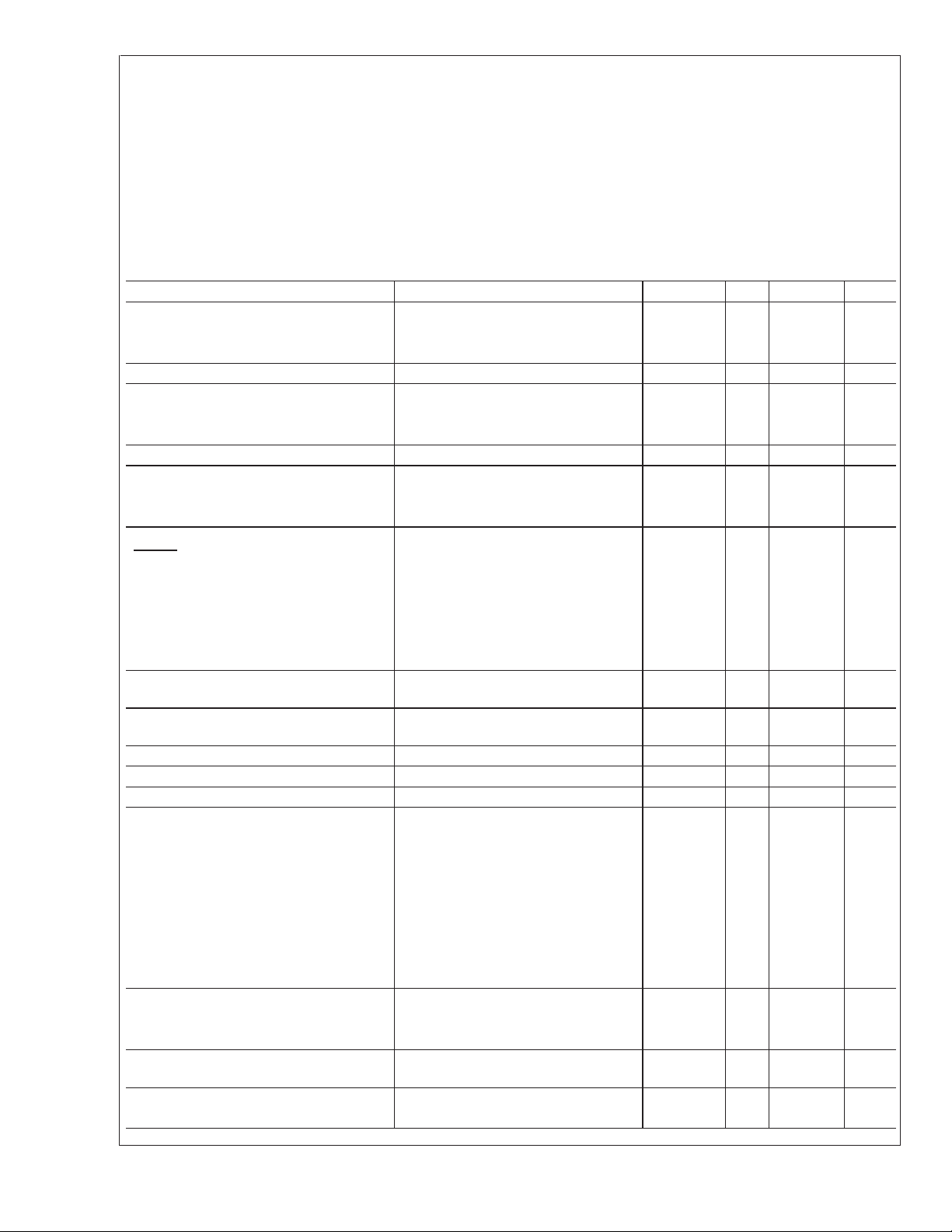
DC Electrical Characteristics
−40˚C ≤ T
A
≤ +85˚C unless otherwise specified.
Parameter Conditions Min Typ Max Units
Operating Voltage 2.7 5.5 V
Power Supply Rise Time 10 50 x 10
6
ns
V
CC
Start Voltage to Guarantee POR 0 0.25 V
Power Supply Ripple (Note 4) Peak-to-Peak 0.1 V
cc
V
Supply Current (Note 5)
CKI = 15 MHz V
CC
= 5.5V, t
C
= 0.67 µs 9.0 mA
CKI = 10 MHz V
CC
= 5.5V, t
C
= 1 µs 6.0 mA
CKI = 4 MHz V
CC
= 4.5V, t
C
= 2.5 µs 2.1 mA
HALT Current (Note 6) V
CC
= 5.5V, CKI=0MHz
<
410 µA
IDLE Current (Note 5)
CKI = 15 MHz V
CC
= 5.5V, t
C
= 0.67 µs 2.25 mA
CKI = 10 MHz V
CC
= 5.5V, t
C
= 1 µs 1.5 mA
CKI = 4 MHz V
CC
= 4.5V, t
C
= 2.5 µs 0.8 mA
Input Levels (V
IH
,V
IL
)
RESET
Logic High 0.8 V
cc
V
Logic Low 0.2 V
cc
V
CKI, All Other Inputs
Logic High 0.7 V
cc
V
Logic Low 0.2 V
cc
V
Internal Bias Resistor for the
Crystal/Resonator Oscillator
0.5 1 2 MΩ
CKI Resistance to V
CC
or GND when R/C
Oscillator is selected
V
CC
= 5.5V 5 8 11 kΩ
Hi-Z Input Leakage V
CC
= 5.5V −2 +2 µA
Input Pullup Current V
CC
= 5.5V, V
IN
= 0V −40 −250 µA
G and L Port Input Hysteresis V
CC
= 5.5V 0.25 V
cc
V
COP8SG Family
www.national.com7
DC Electrical Characteristics (Continued)
−40˚C ≤ T
A
≤ +85˚C unless otherwise specified.
Parameter Conditions Min Typ Max Units
Output Current Levels
D Outputs
Source V
CC
= 4.5V, V
OH
= 3.3V −0.4 mA
V
CC
= 2.7V, V
OH
= 1.8V -0.2 mA
Sink V
CC
= 4.5V, V
OL
= 1.0V 10 mA
V
CC
= 2.7V, V
OL
= 0.4V 2 mA
All Others
Source (Weak Pull-Up Mode) V
CC
= 4.5V, V
OH
= 2.7V −10.0 −110 µA
V
CC
= 2.7V, V
OH
= 1.8V -2.5 -33 µA
Source (Push-Pull Mode) V
CC
= 4.5V, V
OH
= 3.3V −0.4 mA
V
CC
= 2.7V, V
OH
= 1.8V -0.2 mA
Sink (Push-Pull Mode) V
CC
= 4.5V, V
OL
= 0.4V
V
CC
= 2.7V, V
OL
= 0.4V
1.6
0.7
mA
mA
TRI-STATE Leakage V
CC
= 5.5V −2 +2 µA
Allowable Sink Current per Pin (Note 9)
D Outputs and L0 to L3 15 mA
All Others 3mA
Maximum Input Current without Latchup
(Note 7)
Room Temp.
±
200 mA
RAM Retention Voltage, Vr 2.0 V
V
CC
Rise Time from a V
CC
≥ 2.0V (Note 10) 12 µs
EPROM Data Retenton (Note 8), (Note 9) T
A
= 55˚C
>
29 years
Input Capacitance (Note 9) 7 pF
Load Capacitance on D2 (Note 9) 1000 pF
AC Electrical Characteristics
−40˚C ≤ T
A
≤ +85˚C unless otherwise specified.
Parameter Conditions Min Typ Max Units
Instruction Cycle Time (t
C
)
Crystal/Resonator, External 4.5V ≤ V
CC
≤ 5.5V 0.67 µs
2.7V ≤ V
CC
≤ 4.5V 2 µs
R/C Oscillator (Internal) 4.5V ≤ V
CC
≤ 5.5V 2 µs
Frequency Variation (Note 9) 4.5V ≤ V
CC
≤ 5.5V
±
35
%
External CKI Clock Duty Cycle (Note 9) fr = Max 45 55
%
Rise Time (Note 9) fr = 10 MHz Ext Clock 8 ns
Fall Time (Note 9) fr = 10 MHz Ext Clock 5 ns
MICROWIRE Setup Time (t
UWS
) (Note
11)
20 ns
MICROWIRE Hold Time (t
UWH
) (Note
11)
56 ns
MICROWIRE Output Propagation
Delay (t
UPD
) (Note 11)
220 ns
Input Pulse Width (Note 9)
Interrupt Input High Time 1 t
C
Interrupt Input Low Time 1 t
C
Timer 1, 2, 3, Input High Time 1 t
C
Timer 1 2, 3, Input Low Time 1 t
C
Reset Pulse Width 1 µs
Note 3: t
C
= Instruction cycle time.
COP8SG Family
www.national.com 8
AC Electrical Characteristics (Continued)
Note 4: Maximum rate of voltage change must be
<
0.5 V/ms.
Note 5: Supply and IDLE currents are measured with CKI driven with a square wave Oscillator, External Oscillator, inputs connected to V
CC
and outputs driven low
but not connected to a load.
Note 6: The HALTmode will stop CKI from oscillating in the R/C and the Crystal configurations. In the R/C configuration, CKI is forced high internally. In the crystal
or external configuration, CKI is TRI-STATE. Measurement of I
DD
HALT is done with device neither sourcing nor sinking current; with L. F, C, G0, and G2–G5 pro-
grammed as low outputs and not driving a load; all outputs programmed low and not driving a load; all inputs tied to V
CC
; clock monitor disabled. Parameter refers
to HALT mode entered via setting bit 7 of the G Port data register.
Note 7: Pins G6 and RESET are designed with a high voltage input network. These pins allow input voltages
>
V
CC
and the pins will have sink current to V
CC
when
biased at voltages
>
V
CC
(the pins do not have source current when biased at a voltage below V
CC
). The effective resistance to V
CC
is 750Ω (typical). These two
pins will not latch up. The voltage at the pins must be limited to
<
14V.WARNING: Voltages in excess of 14V will cause damage to the pins. This warning excludes
ESD transients.
Note 8: National Semiconductor uses the High Temperature Storage Life (HTSL) test to evaluate the data retention capabilities of the EPROM memory cells used
in our OTP microcontrollers. Qualification devices have been stressed at 150˚C for 1000 hours. Under these conditions, our EPROM cells exhibit data retention ca-
pabilities in excess of 29 years. This is based on an activation energy of 0.7eV derated to 55˚C.
Note 9: Parameter characterized but not tested.
Note 10: Rise times faster than the minimum specification may trigger an internal power-on-reset.
Note 11: MICROWIRE Setup and Hold Times and Propagation Delays are referenced to the appropriate edge of the MICROWIRE clock. See and the MICROWIRE
operation description.
Comparators AC and DC Characteristics
V
CC
= 5V, −40˚C ≤ T
A
≤ +85˚C.
Parameter Conditions Min Typ Max Units
Input Offset Voltage (Note 12) 0.4V ≤ V
IN
≤ V
CC
−
1.5V
±
5
±
15 mV
Input Common Mode Voltage Range 0.4 V
CC
− 1.5 V
Voltage Gain 100 dB
Low Level Output Current V
OL
= 0.4V −1.6 mA
High Level Output Current V
OH
=V
CC
− 0.4V 1.6 mA
DC Supply Current per Comparator
(When Enabled)
150 µA
Response Time (Note 13) 200 mV step input
100 mV Overdrive,
200 ns
100 pF Load
Note 12: The comparator inputs are high impedance port inputs and, as such, input current is limited to port input leakage current.
Note 13: Response time is measured from a step input to a valid logic level at the comparator output. software response time is dependent of instruction execution.
DS101317-9
FIGURE 4. MICROWIRE/PLUS Timing
COP8SG Family
www.national.com9
Absolute Maximum Ratings (Note 2)
If Military/Aerospace specified devices are required,
please contact the National Semiconductor Sales Office/
Distributors for availability and specifications.
Supply Voltage (V
CC
)7V
Voltage at Any Pin −0.3V to V
CC
+0.3V
Total Current into V
CC
Pin (Source) 100 mA
Total Current out of GND
Pin (Sink) 110 mA
Storage Temperature
Range −65˚C to +140˚C
ESD Protection Level 2kV (Human Body Model)
Note 14:
Absolute maximum ratings indicate limits beyond which damage to
the device may occur. DC and AC electrical specifications are not ensured
when operating the device at absolute maximum ratings.
DC Electrical Characteristics
−40˚C ≤ T
A
≤ +125˚C unless otherwise specified.
Parameter Conditions Min Typ Max Units
Operating Voltage 4.5 5.5 V
Power Supply Rise Time 10 50 x 10
6
ns
V
CC
Start Voltage to Guarantee POR 0 0.25 V
Power Supply Ripple (Note 4) Peak-to-Peak 0.1 V
cc
V
Supply Current (Note 5)
CKI = 10 MHz V
CC
= 5.5V, t
C
= 1 µs 6.0 mA
CKI = 4 MHz V
CC
= 4.5V, t
C
= 2.5 µs 2.1 mA
HALT Current (Note 6) V
CC
= 5.5V, CKI=0MHz
<
410 µA
IDLE Current (Note 5)
CKI = 10 MHz V
CC
= 5.5V, t
C
= 1 µs 1.5 mA
CKI = 4 MHz V
CC
= 4.5V, t
C
= 2.5 µs 0.8 mA
Input Levels (V
IH
,V
IL
)
RESET
Logic High 0.8 V
cc
V
Logic Low 0.2 V
cc
V
CKI, All Other Inputs
Logic High 0.7 V
cc
V
Logic Low 0.2 V
cc
V
Internal Bias Resistor for the
Crystal/Resonator Oscillator
0.5 1 2 MΩ
CKI Resistance to V
CC
or GND when R/C
Oscillator is selected
V
CC
= 5.5V 5 8 11 kΩ
Hi-Z Input Leakage V
CC
= 5.5V −5 +5 µA
Input Pullup Current V
CC
= 5.5V, V
IN
= 0V −35 −400 µA
G and L Port Input Hysteresis V
CC
= 5.5V 0.25 V
cc
V
Output Current Levels
D Outputs
Source V
CC
= 4.5V, V
OH
= 3.3V −0.4 mA
Sink V
CC
= 4.5V, V
OL
= 1.0V 9 mA
All Others
Source (Weak Pull-Up Mode) V
CC
= 4.5V, V
OH
= 2.7V −9 −140 µA
Source (Push-Pull Mode) V
CC
= 4.5V, V
OH
= 3.3V −0.4 mA
Sink (Push-Pull Mode) V
CC
= 4.5V, V
OL
= 0.4V 1.4 mA
TRI-STATE Leakage V
CC
= 5.5V −5 +5 µA
Allowable Sink Current per Pin (Note 9)
D Outputs and L0 to L3 15 15 mA
All Others 33mA
Maximum Input Current without Latchup
(Note 7)
Room Temp.
±
200 mA
RAM Retention Voltage, Vr 2.0 V
V
CC
Rise Time from a V
CC
≥ 2.0V (Note 10) 12 µs
COP8SG Family
www.national.com 10
DC Electrical Characteristics (Continued)
−40˚C ≤ T
A
≤ +125˚C unless otherwise specified.
Parameter Conditions Min Typ Max Units
EPROM Data Retenton (Note 8),(Note 9) T
A
= 55˚C
>
29 years
Input Capacitance (Note 9) 7 pF
Load Capacitance on D2 (Note 9) 1000 pF
AC Electrical Characteristics
−40˚C ≤ T
A
≤ +125˚C unless otherwise specified.
Parameter Conditions Min Typ Max Units
Instruction Cycle Time (t
C
)
Crystal/Resonator, External 4.5V ≤ V
CC
≤ 5.5V 1 µs
R/C Oscillator (Internal) 4.5V ≤ V
CC
≤ 5.5V 2 µs
Frequency Variation (Note 9) 4.5V ≤ V
CC
≤ 5.5V
±
35
%
External CKI Clock Duty Cycle (Note 9) fr = Max 45 55
%
Rise Time (Note 9) fr = 10 MHz Ext Clock 12 ns
Fall Time (Note 9) fr = 10 MHz Ext Clock 8 ns
MICROWIRE Setup Time (t
UWS
) (Note
11)
20 ns
MICROWIRE Hold Time (t
UWH
) (Note
11)
56 ns
MICROWIRE Output Propagation
Delay (t
UPD
) (Note 11)
220 ns
Input Pulse Width (Note 9)
Interrupt Input High Time 1 t
C
Interrupt Input Low Time 1 t
C
Timer 1, 2, 3, Input High Time 1 t
C
Timer 1 2, 3, Input Low Time 1 t
C
Reset Pulse Width 1 µs
Comparators AC and DC Characteristics
V
CC
= 5V, −40˚C ≤ T
A
≤ +125˚C.
Parameter Conditions Min Typ Max Units
Input Offset Voltage (Note 12) 0.4V ≤ V
IN
≤ V
CC
−
1.5V
±
5
±
25 mV
Input Common Mode Voltage Range 0.4 V
CC
− 1.5 V
Voltage Gain 100 dB
Low Level Output Current V
OL
= 0.4V −1.6 mA
High Level Output Current V
OH
=V
CC
− 0.4V 1.6 mA
DC Supply Current per Comparator
(When Enabled)
150 µA
Response Time (Note 13) 200 mV step input
100 mV Overdrive,
400 ns
100 pF Load
COP8SG Family
www.national.com11
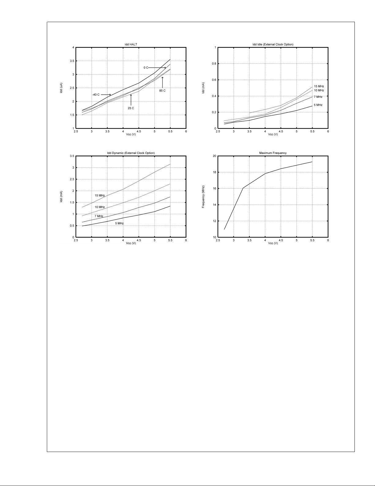
Typical Performance Characteristics T
A
=
25˚C (unless otherwise specified)
DS101317-49 DS101317-50
DS101317-51 DS101317-52
COP8SG Family
www.national.com 12
4.0 Pin Descriptions
The COP8SGx I/O structure enables designers to reconfig-
ure the microcontroller’s I/O functions with a single instruc-
tion. Each individual I/O pin can be independently configured
as output pin low, output high, input with high impedance or
input with weak pull-up device. A typical example is the use
of I/O pins as the keyboard matrix input lines. The input lines
can be programmed with internal weak pull-ups so that the
input lines read logic high when the keys are all open. With
a key closure, the corresponding input line will read a logic
zero since the weak pull-up can easily be overdriven. When
the key is released, the internal weak pull-up will pull the in-
put line back to logic high. This eliminates the need for exter-
nal pull-up resistors. The high current options are available
for driving LEDs, motors and speakers. This flexibility helps
to ensure a cleaner design, with less external components
and lower costs. Below is the general description of all avail-
able pins.
V
CC
and GND are the power supply pins. All V
CC
and GND
pins must be connected.
CKI is the clock input. This can come from the Internal R/C
oscillator, external, or a crystal oscillator (in conjunction with
CKO). See Oscillator Description section.
RESET is the master reset input. See Reset description sec-
tion.
Each device contains four bidirectional 8-bit I/O ports (C, G,
L and F), where each individual bit may be independently
configured as an input (Schmitt trigger inputs on ports L and
G), output or TRI-STATE under program control. Three data
memory address locations are allocated for each of these
I/O ports. Each I/O port has two associated 8-bit memory
mapped registers, the CONFIGURATION register and the
output DATA register. A memory mapped address is also re-
served for the input pins of each I/O port. (See the memory
map for the various addresses associated with the I/O ports.)
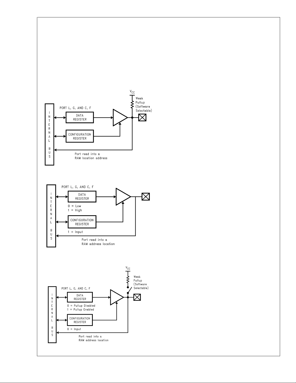
Figure 5
shows the I/O port configurations. The DATA and
CONFIGURATION registers allow for each port bit to be in-
dividually configured under software control as shown below:
CONFIGURATION
Register
DATA
Register
Port Set-Up
0 0 Hi-Z Input
(TRI-STATE Output)
0 1 Input with Weak Pull-Up
1 0 Push-Pull Zero Output
1 1 Push-Pull One Output
Port L is an 8-bit I/O port. All L-pins have Schmitt triggers on
the inputs.
Port L supports the Multi-Input Wake Up feature on all eight
pins. Port L has the following alternate pin functions:
L7 Multi-input Wakeup or T3B (Timer T3B Input)
L6 Multi-input Wakeup or T3A (Timer T3A Input)
L5 Multi-input Wakeup or T2B (Timer T2B Input)
L4 Multi-input Wakeup or T2A (Timer T2A Input)
L3 Multi-input Wakeup and/or RDX (USART Receive)
L2 Multi-input Wakeup or TDX (USART Transmit)
L1 Multi-input Wakeup and/or CKX (USART Clock)
L0 Multi-input Wakeup
Port G is an 8-bit port. Pin G0, G2–G5 are bi-directional I/O
ports. Pin G6 is always a general purpose Hi-Z input. All pins
have Schmitt Triggers on their inputs.Pin G1 serves as the
dedicated WATCHDOG output with weak pullup if
WATCHDOG feature is selected by the Mask Option reg-
ister.The pin is a general purpose I/O if WATCHDOG fea-
ture is not selected. If WATCHDOG feature is selected, bit
1 of the Port G configuration and data register does not have
any effect on Pin G1 setup. Pin G7 is either input or output
depending on the oscillator option selected. With the crystal
oscillator option selected, G7 serves as the dedicated output
pin for the CKO clock output. With the internal R/C or the ex-
ternal oscillator option selected, G7 serves as a general pur-
pose Hi-Z input pin and is also used to bring the device out
of HALT mode with a low to high transition on G7.
Since G6 is an input only pin and G7 is the dedicated CKO
clock output pin (crystal clock option) or general purpose in-
put (R/C or external clock option), the associated bits in the
data and configuration registers for G6 and G7 are used for
special purpose functions as outlined below. Reading the G6
and G7 data bits will return zeroes.
Each device will be placed in the HALTmode by writing a “1”
to bit 7 of the Port G Data Register. Similarly the device will
be placed in the IDLE mode by writing a “1” to bit 6 of the
Port G Data Register.
Writing a “1” to bit 6 of the Port G Configuration Register en-
ables the MICROWIRE/PLUS to operate with the alternate
phase of the SK clock. The G7 configuration bit, if set high,
enables the clock start up delay after HALT when the R/C
clock configuration is used.
Config. Reg. Data Reg.
G7 CLKDLY HALT
G6 Alternate SK IDLE
Port G has the following alternate features:
G7 CKO Oscillator dedicated output or general purpose in-
put
G6 SI (MICROWIRE Serial Data Input)
G5 SK (MICROWIRE Serial Clock)
G4 SO (MICROWIRE Serial Data Output)
G3 T1A (Timer T1 I/O)
G2 T1B (Timer T1 Capture Input)
G1 WDOUT WATCHDOGand/or CLock Monitor if WATCH-
DOG enabled, otherwise it is a general purpose I/O
G0 INTR (External Interrupt Input)
Port C is an 8-bit I/O port. The 40-pin device does not have
a full complement of Port C pins. The unavailable pins are
not terminated. A read operation on these unterminated pins
will return unpredictable values. The 28 pin device do not of-
fer Port C. On this device, the associated Port C Data and
Configuration registers should not be used.
Port F is an 8-bit I/O port. The 28--pin device does not have
a full complement of Port F pins. The unavailable pins are
not terminated. A read operation on these unterminated pins
will return unpredictable values.
Port F1–F3 are used for Comparator 1. Port F4–F6 are used
for Comparator 2.
The Port F has the following alternate features:
F6 COMP2OUT (Comparator 2 Output)
F5 COMP2+IN (Comparator 2 Positive Input)
F4 COMP2-IN (Comparator 2 Negative Input)
F3 COMP1OUT (Comparator 1 Output)
F2 COMP1+IN (Comparator 1 Positive Input)
F1 COMP1-IN (Comparator 1 Negative Input)
Note: For compatibility with existing software written for COP888xG devices
and with existing Mask ROM devices, a read of the Port I input pins
COP8SG Family
www.national.com13
4.0 Pin Descriptions (Continued)
(address xxD7) will return the same data as reading the Port F input
pins (address xx96). It is recommended new applications which will go
to production with the COP8SGx use the Port F addresses. Note that
compatible ROM devices contains the input only Port I instead of the
bi-directional Port F.
Port D is an 8-bit output port that is preset high when RESET
goes low. The user can tie two or more D port outputs (ex-
cept D2) together in order to get a higher drive.
Note: Care must be exercised with the D2 pin operation. At RESET, the ex-
ternal loads on this pin must ensure that the output voltages stay
above 0.7 V
CC
to prevent the chip from entering special modes. Also
keep the external loading on D2 to less than 1000 pF.
5.0 Functional Description
The architecture of the devices are a modified Harvard archi-
tecture. With the Harvard architecture, the program memory
ROM is separated from the data store memory (RAM). Both
ROM and RAM have their own separate addressing space
with separate address buses. The architecture, though
based on the Harvard architecture, permits transfer of data
from ROM to RAM.
5.1 CPU REGISTERS
The CPU can do an 8-bit addition, subtraction, logical or shift
operation in one instruction (t
C
) cycle time.
There are six CPU registers:
A is the 8-bit Accumulator Register
PC is the 15-bit Program Counter Register
PU is the upper 7 bits of the program counter (PC)
PL is the lower 8 bits of the program counter (PC)
B is an 8-bit RAM address pointer, which can be optionally
post auto incremented or decremented.
X is an 8-bit alternate RAM address pointer, which can be
optionally post auto incremented or decremented.
S is the 8-bit Segment Address Register used to extend the
lower half of the address range (00 to 7F) into 256 data seg-
ments of 128 bytes each.
SP is the 8-bit stack pointer, which points to the subroutine/
interrupt stack (in RAM). With reset the SP is initialized to
RAM address 02F Hex (devices with 64 bytes of RAM), or
initialized to RAM address 06F Hex (devices with 128 bytes
of RAM).
All the CPU registers are memory mapped with the excep-
tion of the Accumulator (A) and the Program Counter (PC).
5.2 PROGRAM MEMORY
The program memory consists of varies sizes of ROM.
These bytes may hold program instructions or constant data
(data tables for the LAID instruction, jump vectors for the JID
instruction, and interrupt vectors for the VIS instruction). The
program memory is addressed by the 15-bit program
counter (PC). All interrupts in the device vector to program
memory location 0FF Hex. The contents of the program
memory read 00 Hex in the erased state. Program execution
starts at location 0 after RESET.
5.3 DATA MEMORY
The data memory address space includes the on-chip RAM
and data registers, the I/O registers (Configuration, Data and
Pin), the control registers, the MICROWIRE/PLUS SIO shift
register, and the various registers, and counters associated
with the timers (with the exception of the IDLE timer). Data
memory is addressed directly by the instruction or indirectly
by the B, X and SP pointers.
The data memory consists of 256 or 512 bytes of RAM. Six-
teen bytes of RAM are mapped as “registers” at addresses
0F0 to 0FE Hex. These registers can be loaded immediately,
and also decremented and tested with the DRSZ (decrement
register and skip if zero) instruction. The memory pointer
registers X, SP and B are memory mapped into this space at
address locations 0FC to 0FE Hex respectively, with the
other registers (except 0FF) being available for general us-
age.
The instruction set permits any bit in memory to be set, reset
or tested. All I/O and registers (except A and PC) are
DS101317-10
FIGURE 5. I/O Port Configurations
DS101317-12
FIGURE 6. I/O Port Configurations — Output Mode
DS101317-11
FIGURE 7. I/O Port Configurations — Input Mode
COP8SG Family
www.national.com 14
5.0 Functional Description (Continued)
memory mapped; therefore, I/O bits and register bits can be
directly and individually set, reset and tested. The accumula-
tor (A) bits can also be directly and individually tested.
Note: RAM contents are undefined upon power-up.
5.4 DATA MEMORY SEGMENT RAM EXTENSION
Data memory address 0FF is used as a memory mapped lo-
cation for the Data Segment Address Register (S).
The data store memory is either addressed directly by a
single byte address within the instruction, or indirectly rela-
tive to the reference of the B, X, or SP pointers (each con-
tains a single-byte address). This single-byte address allows
an addressing range of 256 locations from 00 to FF hex. The
upper bit of this single-byte address divides the data store
memory into two separate sections as outlined previously.
With the exception of the RAM register memory from ad-
dress locations 00F0 to 00FF, all RAM memory is memory
mapped with the upper bit of the single-byte address being
equal to zero. This allows the upper bit of the single-byte ad-
dress to determine whether or not the base address range
(from 0000 to 00FF) is extended. If this upper bit equals one
(representing address range 0080 to 00FF), then address
extension does not take place. Alternatively, if this upper bit
equals zero, then the data segment extension register S is
used to extend the base address range (from 0000 to 007F)
from XX00 to XX7F,where XX represents the 8 bits from the
S register. Thus the 128-byte data segment extensions are
located from addresses 0100 to 017F for data segment 1,
0200 to 027F for data segment 2, etc., up to FF00 to FF7F
for data segment 255. The base address range from 0000 to
007F represents data segment 0.
Figure 8
illustrates how the S register data memory exten-
sion is used in extending the lower half of the base address
range (00 to 7F hex) into 256 data segments of 128 bytes
each, with a total addressing range of 32 kbytes from XX00
to XX7F. This organization allows a total of 256 data seg-
ments of 128 bytes each with an additional upper base seg-
ment of 128 bytes. Furthermore, all addressing modes are
available for all data segments. The S register must be
changed under program control to move from one data seg-
ment (128 bytes) to another. However, the upper base seg-
ment (containing the 16 memory registers, I/O registers,
control registers, etc.) is always available regardless of the
contents of the S register, since the upper base segment
(address range 0080 to 00FF) is independent of data seg-
ment extension.
The instructions that utilize the stack pointer (SP) always ref-
erence the stack as part of the base segment (Segment 0),
regardless of the contents of the S register. The S register is
not changed by these instructions. Consequently, the stack
(used with subroutine linkage and interrupts) is always lo-
cated in the base segment. The stack pointer will be initial-
ized to point at data memory location 006F as a result of re-
set.
The 128 bytes of RAM contained in the base segment are
split between the lower and upper base segments. The first
112bytes of RAM are resident from address 0000 to 006F in
the lower base segment, while the remaining 16 bytes of
RAM represent the 16 data memory registers located at ad-
dresses 00F0 to 00FF of the upper base segment. No RAM
is located at the upper sixteen addresses (0070 to 007F) of
the lower base segment.
Additional RAM beyond these initial 128 bytes, however, will
always be memory mapped in groups of 128 bytes (or less)
at the data segment address extensions (XX00 to XX7F) of
the lower base segment. The additional 384 bytes of RAM in
this device are memory mapped at address locations 0100
to 017F, 0200 to 027F and 0300 to 037F hex.
DS101317-45
FIGURE 8. RAM Organization
COP8SG Family
www.national.com15
5.0 Functional Description (Continued)
Memory address ranges 0200 to 027F and 0300 to 037F are
unavailable on the COP8SGx5 and, if read, will return under-
fined data.
5.5 ECON (CONFIGURATION) REGISTER
For compatibility with COP8SGx7 devices, mask options are
defined by an ECON Configuration Register which is pro-
grammed at the same time as the program code. Therefore,
the register is programmed at the same time as the program
memory.
The format of the ECON register is as follows:
Bit 7 Bit 6 Bit 5 Bit 4 Bit 3 Bit 2 Bit 1 Bit 0
X POR SECURITY CKI 2 CKI 1 WATCH F-Port HALT
DOG
Bit 7 = x This is for factory test. The polarity is “Don’t
Care.”
Bit 6 = 1 Power-on reset enabled.
= 0 Power-on reset disabled.
Bit 5 = 1 Security enabled.
Bits 4,3=0,0 External CKI option selected. G7 is avail-
able as a HALT restart and/or general pur-
pose input. CKI is clock input.
= 0, 1 R/C oscillator option selected. G7 is avail-
able as a HALT restart and/or general pur-
pose input. CKI clock input. Internal R/C
components are supplied for maximum R/C
frequency.
= 1, 0 Crystal oscillator with on-chip crystal bias
resistor disabled. G7 (CKO) is the clock
generator output to crystal/resonator.
= 1, 1 Crystal oscillator with on-chip crystal bias
resistor enabled. G7 (CKO) is the clock
generator output to crystal/resonator.
Bit 2 = 1 WATCHDOGfeature disabled. G1 is a gen-
eral purpose I/O.
= 0 WATCHDOG feature enabled. G1 pin is
WATCHDOG output with weak pullup.
Bit 1 = 1 Force port I compatibility. Disable port F
outputs and pull-ups. This is intended for
compatibility with existing code and Mask
ROMMed devices only. This bit should be
programmed to 0 for all other applications.
= 0 Enable full port F capability.
Bit 0 = 1 HALT mode disabled.
= 0 HALT mode enabled.
5.6 USER STORAGE SPACE IN EPROM
The ECON register is outside of the normal address range of
the ROM and can not be accessed by the executing soft-
ware.
The COP8 assembler defines a special ROM section type,
CONF, into which the ECON may be coded. Both ECON and
User Data are programmed automatically by programmers
that are certified by National.
The following examples illustrate the declaration of ECON
and the User information.
Syntax:
[label:] .sect econ, conf
.db value ;1 byte,
;configures options
.db <user information>
.endsect ; up to 8 bytes
Example: The following sets a value in the ECON register
and User Identification for a COP8SGR728M7. The ECON
bit values shown select options: Power-on enabled, Security
disabled, Crystal oscillator with on-chip bias disabled,
WATCHDOG enabled and HALT mode enabled.
.sect econ, conf
.db 0x55 ;por, xtal, wd, halt
.db 'my v1.00' ;user data declaration
.endsect
5.7 OTP SECURITY
The device has a security feature that, when enabled, pre-
vents external reading of the OTP program memory. The se-
curity bit in the ECON register determines, whether security
is enabled or disabled. If the security feature is disabled, the
contents of the internal EPROM may be read.
If the security feature is enabled, then any attempt to ex-
ternally read the contents of the EPROM will result in the
value FF Hex being read from all program locations Un-
der no circumstances can a secured part be read. In ad-
dition, with the security feature enabled, the write operation
to the EPROM program memory and ECON register is inhib-
ited. The ECON register is readable regardless of the state
of the security bit. The security bit, when set, cannot be
erased, even in windowed packages. If the security bit is
set in a device in a windowed package, that device may be
erased but will not be further programmable.
If security is being used, it is recommended that all other bits
in the ECON register be programmed first. Then the security
bit can be programmed.
5.8 ERASURE CHARACTERISTICS
The erasure characteristics of the device are such that era-
sure begins to occur when exposed to light with wavelengths
shorter than approximately 4000 Angstroms (Ar ). It should be
noted that sunlight and certain types of fluorescent lamps
have wavelengths in the 3000Ar - 4000Ar range.
After programming, opaque labels should be placed over the
window of windowed devices to prevent unintentional era-
sure. Covering the window will also prevent temporary func-
tional failure due to the generation of photo currents.
The recommended erasure procedure for windowed devices
is exposure to short wave ultraviolet light which has a wave-
length of 2537 Angstroms (Ar). The integrated dose (i.e. UV
intensity X exposure time) for erasure should be a minimum
of 15W-sec/cm
2
.
5.9 RESET
The devices are initialized when the RESET pin is pulled low
or the On-chip Power-On Reset is enabled.
COP8SG Family
www.national.com 16
5.0 Functional Description (Continued)
The following occurs upon initialization:
Port L: TRI-STATE (High Impedance Input)
Port C: TRI-STATE (High Impedance Input)
Port G: TRI-STATE (High Impedance Input)
Port F: TRI-STATE (High Impedance Input)
Port D: HIGH
PC: CLEARED to 0000
PSW, CNTRL and ICNTRL registers: CLEARED
SIOR:
UNAFFECTED after RESET with power already applied
RANDOM after RESET at power-on
T2CNTRL: CLEARED
T3CNTRL: CLEARED
Accumulator, Timer 1, Timer 2 and Timer 3:
RANDOM after RESET with crystal clock option
(power already applied)
UNAFFECTED after RESET with R/C clock option
(power already applied)
RANDOM after RESET at power-on
WKEN, WKEDG: CLEARED
WKPND: RANDOM
SP (Stack Pointer):
Initialized to RAM address 06F Hex
B and X Pointers:
UNAFFECTED after RESET with power already applied
RANDOM after RESET at power-on
S Register: CLEARED
RAM:
UNAFFECTED after RESET with power already applied
RANDOM after RESET at power-on
USART:
PSR, ENU, ENUR, ENUI: Cleared except the TBMT bit
which is set to one.
COMPARATORS:
CMPSL; CLEARED
WATCHDOG (if enabled):
The device comes out of reset with both the WATCH-
DOG logic and the Clock Monitor detector armed, with the
WATCHDOG service window bits set and the Clock Monitor
bit set. The WATCHDOG and Clock Monitor circuits are in-
hibited during reset. The WATCHDOG service window bits
being initialized high default to the maximum WATCHDOG
service window of 64k t
C
clock cycles. The Clock Monitor bit
being initialized high will cause a Clock Monitor error follow-
ing reset if the clock has not reached the minimum specified
frequency at the termination of reset. A Clock Monitor error
will cause an active low error output on pin G1. This error
output will continue until 16 t
C
–32 t
C
clock cycles following
the clock frequency reaching the minimum specified value,
at which time the G1 output will go high.
5.9.1 External Reset
The RESET input when pulled low initializes the device. The
RESET pin must be held low for a minimum of one instruc-
tion cycle to guarantee a valid reset. During Power-Up initial-
ization, the user must ensure that the RESET pin is held low
until the device is within the specified V
CC
voltage. An R/C
circuit on the RESET pin with a delay 5 times (5x) greater
than the power supply rise time or 15 µs whichever is
greater,is recommended. Reset should also be wide enough
to ensure crystal start-up upon Power-Up.
RESET may also be used to cause an exit from the HALT
mode.
A recommended reset circuit for this device is shown in
Fig-
ure 10
.
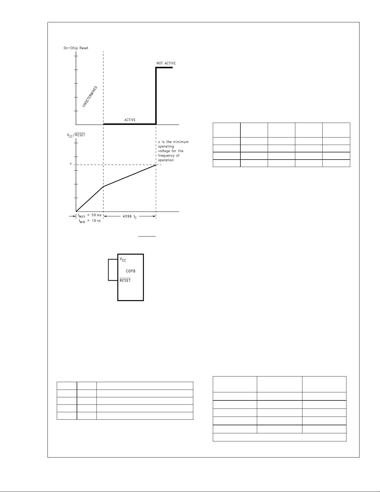
5.9.2 On-Chip Power-On Reset
The on-chip reset circuit is selected by a bit in the ECON reg-
ister. When enabled, the device generates an internal reset
as V
CC
rises to a voltage level above 2.0V. The on-chip reset
circuitry is able to detect both fast and slow rise times on V
CC
(V
CC
rise time between 10 ns and 50 ms).To guarantee an
on-chip power-on-reset, V
CC
must start at a voltage less than
the start voltage specified in the DC characteristics. Also, if
V
CC
be lowered to the start voltage before powering back up
to the operating range. If this is not possible, it is recom-
mended that external reset be used.
Under no circumstances should the RESET pin be allowed
to float. If the on-chip Power-On Reset feature is being used,
RESET pin should be connected directly, or through a
pull-up resistor, to V
CC
. The output of the power-on reset de-
tector will always preset the Idle timer to 0FFF(4096 t
C
). At
this time, the internal reset will be generated.
If the Power-On Reset feature is enabled, the internal reset
will not be turned off until the Idle timer underflows. The inter-
nal reset will perform the same functions as external reset.
The user is responsible for ensuring that V
CC
is at the mini-
mum level for the operating frequency within the 4096 t
C
. Af-
ter the underflow, the logic is designed such that no addi-
tional internal resets occur as long as V
CC
remains above
2.0V.
The contents of data registers and RAM are unknown follow-
ing the on-chip reset.
DS101317-13
FIGURE 9. Reset Logic
DS101317-14
RC
>
5x power supply rise time or 15 µs, whichever is greater.
FIGURE 10. Reset Circuit Using External Reset
COP8SG Family
www.national.com17
5.0 Functional Description (Continued)
5.10 OSCILLATOR CIRCUITS
There are four clock oscillator options available: Crystal Os-
cillator with or without on-chip bias resistor, R/C Oscillator
with on-chip resistor and capacitor, and External Oscillator.
The oscillator feature is selected by programming the ECON
register, which is summarized in
Table 1
.
TABLE 1. Oscillator Option
ECON4 ECON3 Oscillator Option
0 0 External Oscillator
1 0 Crystal Oscillator without Bias Resistor
0 1 R/C Oscillator
1 1 Crystal Oscillator with Bias Resistor
5.10.1 Crystal Oscillator
The crystal Oscillator mode can be selected by programming
ECON Bit 4 to 1. CKI is the clock input while G7/CKO is the
clock generator output to the crystal. An on-chip bias resistor
connected between CKI and CKO can be enabled by pro-
gramming ECON Bit 3 to 1 with the crystal oscillator option
selection. The value of the resistor is in the range of 0.5M to
2M (typically 1.0M).
Table 2
shows the component values re-
quired for various standard crystal values. Resistor R2 is
only used when the on-chip bias resistor is disabled.
Figure
13
shows the crystal oscillator connection diagram.
TABLE 2. Crystal Oscillator Configuration,
T
A
= 25˚C, V
CC
=5V
R1 (kΩ)R2(MΩ) C1 (pF) C2 (pF)
CKI Freq.
(MHz)
0 1 18 18 15
0 1 20 20 10
0 1 25 25 4
5.6 1 100 100–156 0.455
5.10.2 External Oscillator
The External Oscillator mode can be selected by program-
ming ECON Bit 3 to 0 and ECON Bit 4 to 0. CKI can be
driven by an external clock signal provided it meets the
specified duty cycle, rise and fall times, and input levels. G7/
CKO is available as a general purpose input G7 and/or Halt
control.
Figure 14
shows the external oscillator connection
diagram.
5.10.3 R/C Oscillator
The R/C Oscillator mode can be selected by programming
ECON Bit 3 to 1 and ECON Bit 4 to 0. In R/C oscillation
mode, CKI is left floating, while G7/CKO is available as a
general purpose input G7 and/or HALT control. The R/C con-
trolled oscillator has on-chip resistor and capacitor for maxi-
mum R/C oscillator frequency operation. The maximum fre-
quency is 5 MHz
±
35
%
for V
CC
between 4.5V to 5.5V and
temperature range of −40˚C to +85˚C. For max frequency
operation, the CKI pin should be left floating. For lower fre-
quencies, an external capacitor should be connected be-
tween CKI and either V
CC
or GND. Immunity of the R/C os-
cillator to external noise can be improved by connecting one
half the external capacitance to V
CC
and one half to GND.
PC board trace length on the CKI pin should be kept as short
as possible.
Table 3
shows the oscillator frequency as a
function of external capacitance on the CKI pin.
Figure 15
shows the R/C oscillator configuration.
TABLE 3. R/C Oscillator Configuration,
−40˚C to +85˚C, V
CC
= 4.5V to 5.5V,
OSC Freq. Variation of
±
35
%
External
Capacitor (pF)*
R/C OSC Freq
(MHz)
Instr. Cycle
(µs)
0 5 2.0
9 4 2.5
52 2 5.0
125 1 10
6100 32 kHz 312.5
* Assumes 3-5 pF board capacitance.
DS101317-15
FIGURE 11. Reset Timing (Power-On Reset Enabled)
with V
CC
Tied to RESET
DS101317-16
FIGURE 12. Reset Circuit Using Power-On Reset
COP8SG Family
www.national.com 18
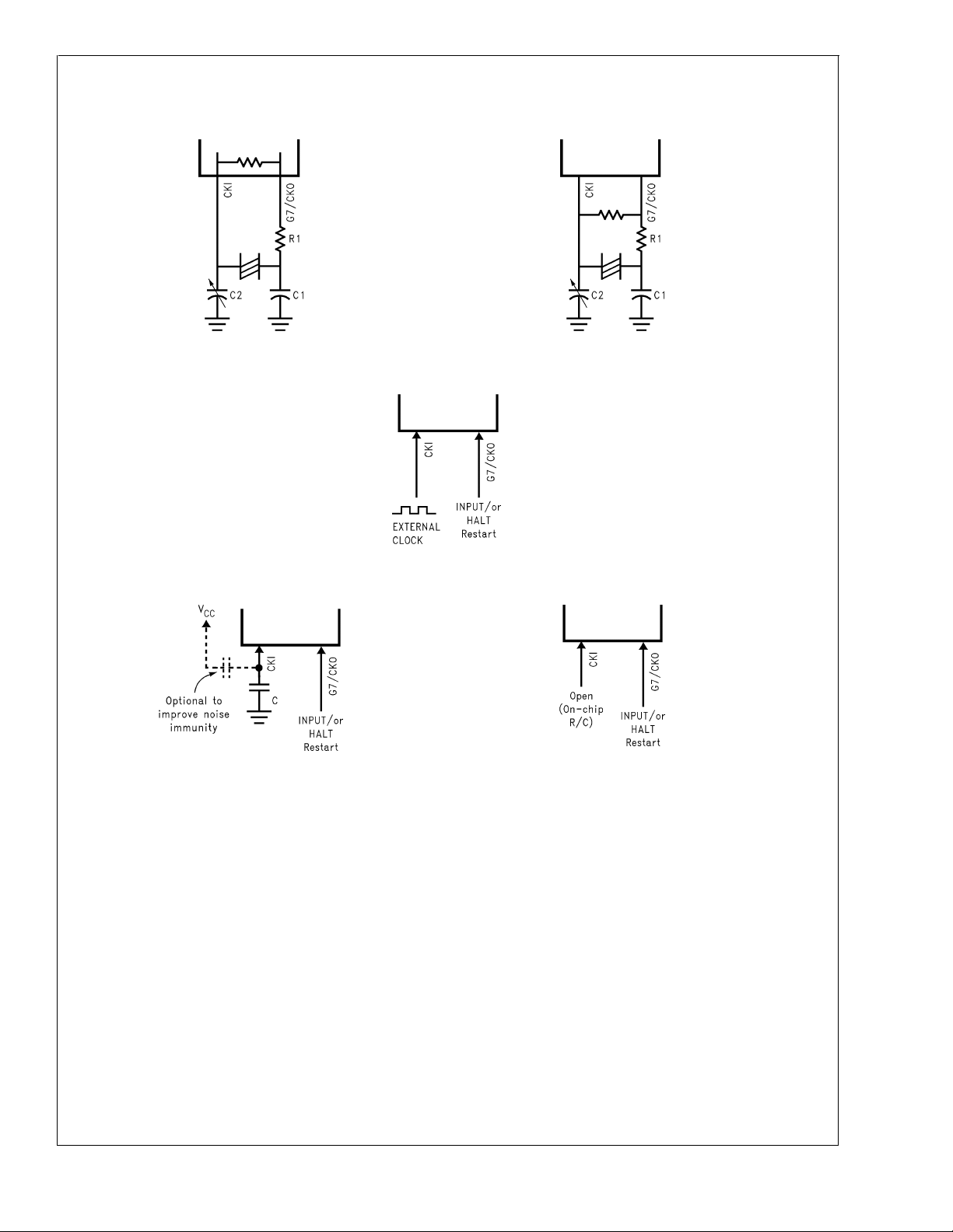
5.0 Functional Description (Continued)
With On-Chip Bias Resistor
DS101317-17
Without On-Chip Bias Resistor
DS101317-18
FIGURE 13. Crystal Oscillator
DS101317-19
FIGURE 14. External Oscillator
DS101317-20
For operation at lower than maximum R/C oscillator frequency.
DS101317-21
For operation at maximum R/C oscillator frequency.
FIGURE 15. R/C Oscillator
COP8SG Family
www.national.com19
 Loading...