


DP8441VLJ-40
DP8440-40/DP8440-25/DP8441-40/DP8441-25
microCMOS Programmable 16/64 Mbit
Dynamic RAM Controller/Driver
February 1995
DP8440-40/DP8440-25/DP8441-40/DP8441-25 microCMOS Programmable 16/64 Mbit
Dynamic RAM Controller/Driver
General Description
The DP8440/41 Dynamic RAM Controllers provide an easy
interface between dynamic RAM arrays and 8-, 16-, 32- and
64-bit microprocessors. The DP8440/41 DRAM Controllers
generate all necessary control and timing signals to successfully interface and design dynamic memory systems.
With significant enhancements over the DP8420/21/22
predecessors, the DP8440/41 are suitable for high performance memory systems. These controllers support page and
burst accesses for fast page, static column and nibble
DRAMs. Refreshes and accesses are arbitrated on chip.
RAS
low time during refresh and RAS precharge time are
guaranteed by these controllers. Separate precharge counters for each RAS
output avoid delayed back to back accesses due to precharge when using memory interleaving.
Programmable features make the DP8440/41 DRAM Controllers flexible enough to fit many memory systems.
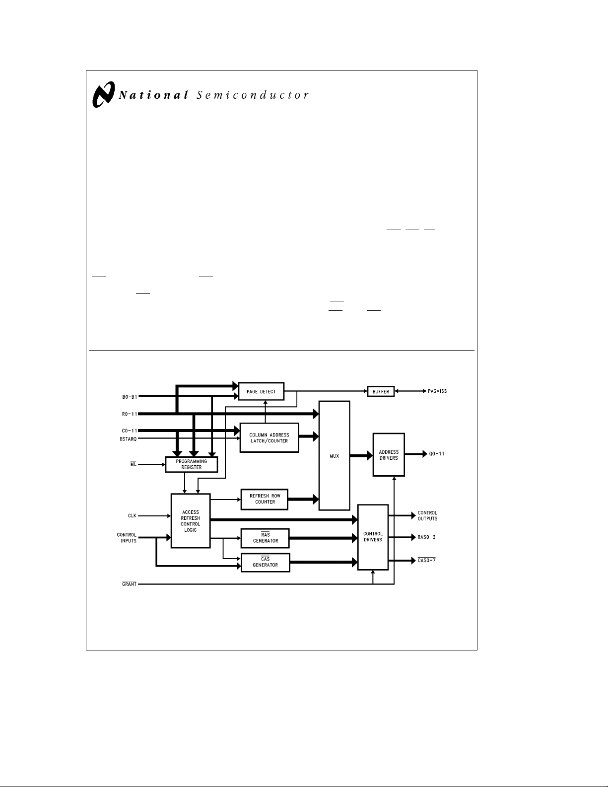
Block Diagram
Features
Y
40 MHz and 25 MHz operation
Y
Page detection
Y
Automatic CPU burst accesses
Y
Support 1/4/16/64 Mbits DRAMs
Y
High capacitance drivers for RAS, CAS,WEand Q outputs
Y
Support for fast page, static column and nibble mode
DRAMs
Y
High precision PLL based delay line
Y
Byte enable for word size up to 32 bits on the DP8440
or 64 bits on the DP8441
Y
Automatic Internal Refresh
Y
Staggered RAS-Only refresh
Y
Burst and CAS-before-RAS refresh
Y
Error scrubbing during refresh
Y
TRI-STATEÉoutputs
Y
Easy interface to all major microprocessors
FIGURE 1
TL/F/11718– 1
TRI-STATEÉis a registered trademark of National Semiconductor Corporation.
C
1995 National Semiconductor Corporation RRD-B30M75/Printed in U. S. A.
TL/F/11718
DRAM Maximum Clock Package Bus Width Largest DRAM
Controller Frequency Type Supporting Possible
DP8440V-40 40 MHz 84-Pin PLCC 8, 16, 32 16 Mbits
DP8440VLJ-40 40 MHz 100-Pin PQFP 8, 16, 32 16 Mbits
DP8440VLJ-25 25 MHz 100-Pin PQFP 8, 16, 32 16 Mbits
DP8441VLJ-40 40 MHz 100-Pin PQFP 8, 16, 32, 64 64 Mbits
DP8441VLJ-25 25 MHz 100-Pin PQFP 8, 16, 32, 64 64 Mbits
Table of Contents
1.0 CONNECTION DIAGRAMS
2.0 FUNCTIONAL INTRODUCTION
3.0 SIGNAL DESCRIPTION
3.1 Address and Control Signals
3.2 DRAM Control Signals
3.3 Refresh Signals
3.4 Reset and Programming Signals
3.5 Clock Inputs
3.6 Power Signals and Capacitor Input
4.0 PROGRAMMING AND RESETTING
4.1 Reset
4.2 Programming Sequence
4.3 Programming Selection Bits
5.0 ACCESS MODES
5.1 Opening Access
5.2 Normal Mode
5.3 Page Mode
5.4 Burst Access
5.5 Inner Page Burst Access
6.0 REFRESH MODES
6.1 Auto-Internal Refresh
6.2 Externally Controlled Refresh
6.3 Error Scrubbing during Refresh
6.4 Extending Refresh
6.5 Refresh Types
7.0 WAIT SUPPORT
7.1 DTACK
7.2 DTACK
7.3 DTACK
7.4 Next Address or Early DTACK
8.0 ABSOLUTE MAXIMUM RATINGS
9.0 DC ELECTRICAL CHARACTERISTICS
10.0 LOAD CAPACITANCE
11.0 AC TIMING PARAMETERS
12.0 AC TIMING WAVEFORMS
CLK and DECLK Timing
Refresh Timing
Refresh and Access Timing
Programming and Initialization Period Timing
Normal Mode Access Timing
Page Mode Access Timing
Burst Mode Access Timing
13.0 ERRATA
14.0 PHYSICAL DIMENSIONS
During Opening Access
During Page Access
During Burst Access
Support
2
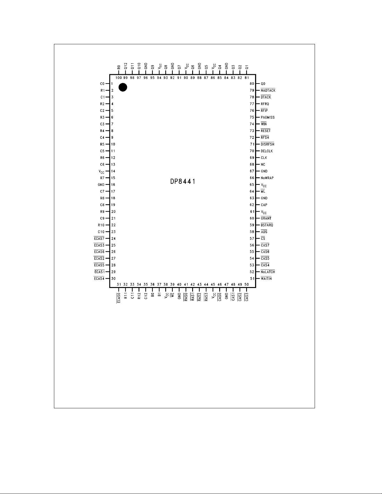
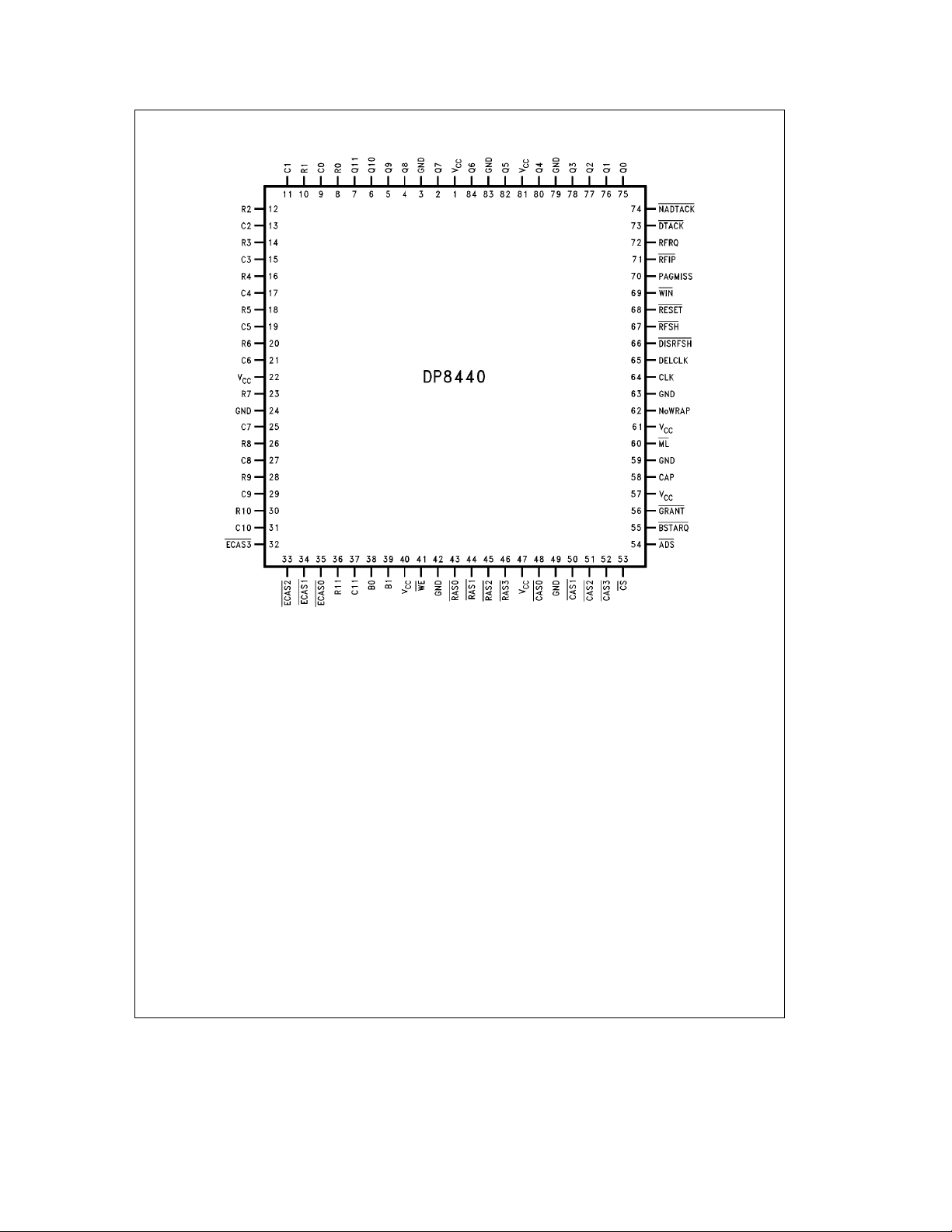
1.0 Connection Diagrams
Top View
FIGURE 2
Order Number DP8441VLJ-40 (40 MHz Operation), DP8441VLJ-25 (25 MHz Operation)
See NS Package Number VLJ100A
3
TL/F/11718– 2
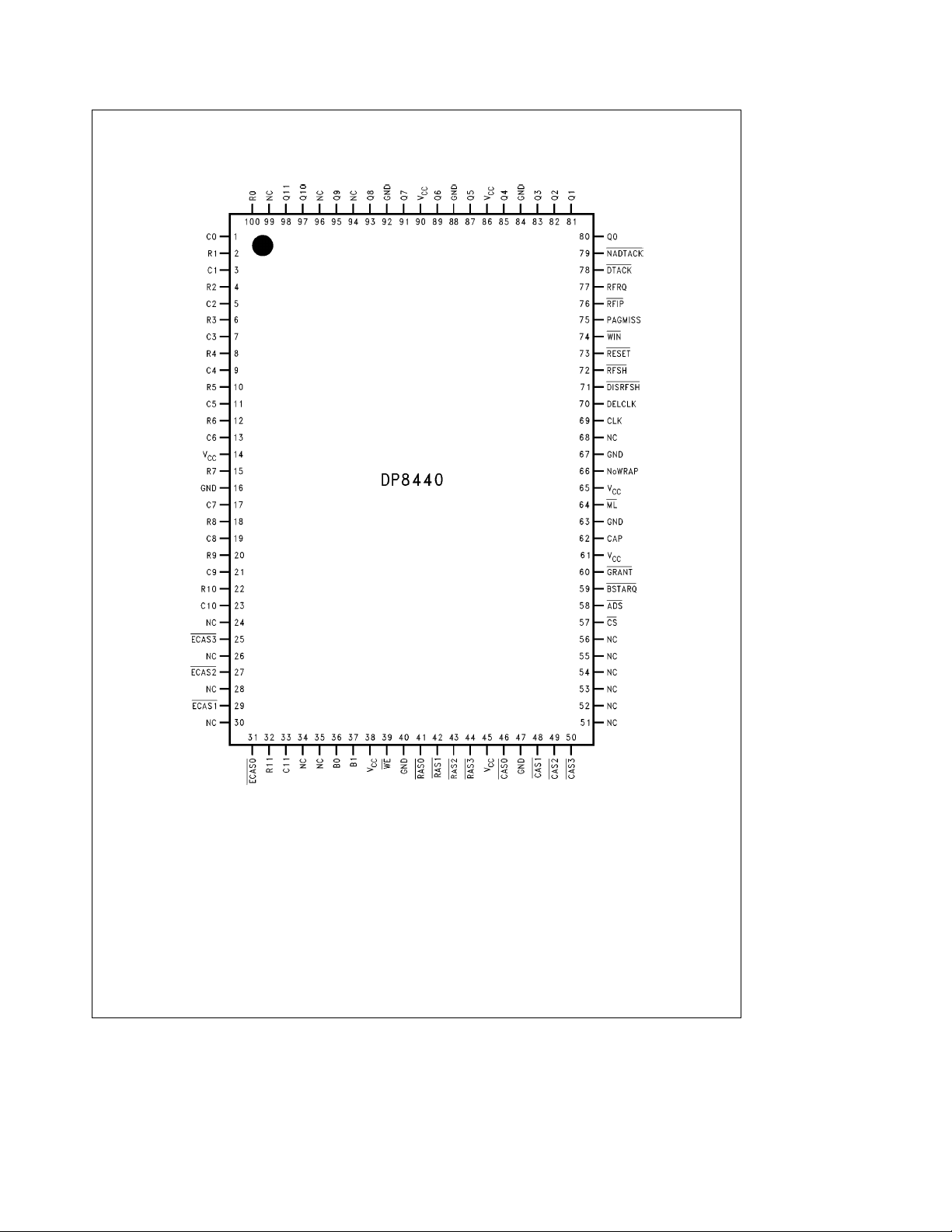
1.0 Connection Diagrams (Continued)
Top View
FIGURE 3
Order Number DP8440VLJ-40 (40 MHz Operation), DP8440VLJ-25 (25 MHz Operation)
See NS Package Number VLJ100A
4
TL/F/11718– 38
1.0 Connection Diagrams (Continued)
Top View
FIGURE 4
Order Number DP8440V-40 (40 MHz Operation)
See NS Package Number V84A
5
TL/F/11718– 3

2.0 Functional Introduction
Reset and Programming: After the power up, the
DP8440/41 must be reset and programmed before it can be
used to access the DRAM. The chip is programmed through
the address bus.
Initialization Period: After programming, the DP8440/41
enter a 60 ms initialization period. During this time the
DP8440/41 perform refreshes to the DRAM. Further warm
up cycles are unnecessary. The user must wait until the
initialization is over to access the memory.
Modes of Operation: The DP8440/41 are synchronous
DRAM controllers. Every access is synchronized to the system clock. The controllers can be programmed in Page
Mode or Normal Mode. Burst accesses are dynamically requested through the input BSTARQ.
Opening Access: They involve a new row address. Regardless of the access mode programmed, opening accesses
behave in the same way. ADS
every access. After asserting the ADS
assert RAS
DP8440/41 will hold the row address on the DRAM address
bus and guarantee that the row address is held for the Row
Address Hold Time (t
ler will then switch the internal multiplexor to place the column address on the DRAM address bus and assert CAS
DTACK
fore asserting to indicate the end of the access.
Normal Access: If the controller is programmed in Normal
Mode (B1
grammed RAS
if desired.
Page Access: The DP8440/41 have an internal page comparator. This feature enables the user to do a series of accesses without negating RAS
remains unchanged. The user needs to provide a new address for every access. The page comparator can also be
programmed as an input. This is beneficial for CPUs that
have an internal page comparator. The user can do burst
accesses while in page if desired.
from the next rising edge of the CLK. The
RAH
will wait the programmed number of wait states be-
e
1), RAS will assert and negate after the prolow time. The user can perform burst access
and CS initiate and qualify
, the DP8440/41 will
) programmed. The DRAM control-
for as long as the row address
Burst Access: These controllers can also generate new
addresses to burst a specific number of locations. The user
can choose to burst in a wrap around fashion for 2, 4, 8, 16
locations. Or, if the input NoWRAP is asserted, the controller will burst consecutive locations and the column address
will not wrap around. The controller must be programmed in
Latch Mode to generate the burst addresses.
Refresh Modes: The DP8440/41 can perform Automatic
Internal Refreshes, or Externally Controlled Refreshes. During a long page access the controller can queue up to six
refresh requests and burst refresh the addresses missed
when the access finishes.
Refresh Types: The DP8440/41 can be programmed to do
all RAS
Refresh, Staggered Refresh, Error Scrubbing during
Refresh or CAS
Wait Support: These controllers provide wait logic for all
three types of accesses. The user needs to program the
desired number of wait states for opening, page and burst
accesses.
RAS
and CAS Configurations: The RAS outputs can be
programmed to drive one, two or four banks of memory and
the CAS
es up to 64 bits wide.
.
TRI-STATE Outputs and Multiporting: The GRANT
can be used for multi-porting. When high this input will
TRI-STATE the outputs, allowing another controller to drive
the DRAM.
Other Features: Independent RAS
low memory interleaving, thus back to back access to different memory banks is not delayed due to precharge.
The output NADTACK
getting the next access to start one clock early.
The input NoWRAP will increment the address during a
burst access in a linear fashion. This is convenient for
graphics or long page access.
Terminology: This paragraph explains the terminology
used in this data sheet. The terms negated and asserted are
used. For example, ECAS0
put is at logic 0. The term NoWRAP asserted means that
NoWRAP is at logic 1.
-before-RAS refresh.
drivers can be programmed for byte writing in bus-
precharge counters al-
can be used to pipeline one address,
asserted means the ECAS0 in-
input
6

3.0 Signal Descriptions
3.1 ADDRESS AND CONTROL SIGNALS
Pin Device (if not Input/
Name Applicable to All) Output
R0–11 DP8440 I ROW ADDRESS: These inputs are used to specify the row address during an access to
R0–12 DP8441
C0–11 DP8440 I COLUMN ADDRESS: These inputs are used to specify the column address during an
C0–12 DP8441
B0–B1 I BANK SELECT: Depending on programming, these inputs are used to select group RAS
ECAS0–3 DP8440 I ENABLE CAS: These inputs asserted enable a single or group of CAS outputs. In
ECAS
0–7 DP8441
NoWRAP I NO WRAP: Asserting this signal causes the column address to be incremented
(EXTNDRF)
NoLATCH DP8441 I COLUMN ADDRESS LATCH DISABLE: This input will disable ADS from latching the
ADS I ADDRESS STROBE: This input starts every access. Depending on programming this input
CS I CHIP SELECT: This input signal must be asserted to enable ADS to start an access.
DTACK O DATA TRANSFER ACKNOWLEDGE: This output can be programmed to insert wait
NADTACK O NEXT ADDRESS or EARLY DTACK: This output asserts one clock cycle before DTACK.
WAITIN DP8441 I WAIT INPUT: This input asserted delays DTACK for one extra clock period.
GRANT I MEMORY ACCESS GRANT: The GRANT input functions as an output enable. If negated,
PAGMISS I/O PAGE MISS: When programmed as an output, this signal asserts when either the row or
BSTARQ/IBURST ACCESS REQUEST: This input enables the Burst Access Mode. This input can be
BSTARQ
the DRAM. They are also used to program the chip when ML
access to the DRAM. They are also used to program the chip when ML
and CAS outputs to assert during an access. They are also used to program the chip when
is asserted.
the ML
combination with the B0, B1 and the programming selection, these inputs select which
CAS
outputs will assert during an access. The ECAS signals can also be used to toggle a
group of CAS
the chip when ML is asserted.
sequentially by one. The column address will not wrap around if NoWRAP is asserted.
When RFIP
of CLK periods until EXTNDRF is negated.
column address when Latch Mode is selected.
could latch the column address from the rising edge.
states into a CPU access cycle. DTACK
signifies that the access has taken place. This signal can be delayed a number of positive
or negative edges of clock. During burst accesses, DTACK
column address.
This output can be used to request the next address in a sort of pipelining fashion or it
provides more time when DTACK
it forces the outputs to a TRI-STATE condition.
the bank address changes from the previous access cycle or the column address has
been incremented beyond the page boundary. If this pin is programmed as an input, it is
the responsibility of the system to tell the controller if the next access is within the page.
Useful for CPUs with internal page comparators, PAGMISS is valid only if ADS
asserted.
programmed to be active high or active low.
outputs during page or burst mode accesses. They are also used to program
is asserted, this signal is an EXTNDRF, used to extend refresh by any number
Description
is asserted.
is asserted.
negated signifies a wait condition, when asserted
transitions increment the
needs to be generated externally.
and CS are
7
3.0 Signal Descriptions (Continued)
3.2 DRAM CONTROL SIGNALS
Pin Device (if not Input/
Name Applicable to All) Output
Q0–11 DP8440 O DRAM ADDRESS: These output signals are the multiplexed outputs of the R0–11/12 and
Q0–12 DP8441
RAS0–3 O ROW ADDRESS STROBES: These outputs are asserted to latch the row address
CAS0–3 DP8440 O COLUMN ADDRESS STROBES: These outputs are asserted to latch the column address
CAS
0–7 DP8441
WE O WRITE ENABLE: This output asserted specifies a write operation to the DRAM. When
WIN I WRITE ENABLE IN: This input is used to signify a write operation to the DRAM. The WE
3.3 REFRESH SIGNALS
Pin Device (if not Input/
Name Applicable to All) Output
RFRQ O REFRESH REQUEST: When RFRQ is asserted, it specifies that 15 msor120ms have
RFIP O REFRESH IN PROGRESS: This output is asserted prior to a refresh cycle and is negated
RFSH I REFRESH: This input asserted with DISRFSH already asserted will request a refresh. If
DISRFSH I DISABLE REFRESH: This input is used to disable internal refreshes and must be asserted
C0–11/12 and form the DRAM address bus. These outputs contain the refresh address
whenever RFIP
resistors.
contained on the outputs Q0–11/12 into the DRAM. When RFIP
outputs are used to latch the refresh row address contained on the Q0–11/12 outputs into
the DRAM. These outputs have high capacitive drivers with 20X series damping resistors.
contained on the outputs Q0–11/12 into the DRAM. When RFIP
before-RAS
the RAS
damping resistors.
negated, this output specifies a read operation to the DRAM. This output has a high
capacitive driver and a 20X series damping resistor.
output will follow this input. Also, this input controls the precharge time for Read and Write
during Burst Mode Access.
passed. If DISRFSH
DP8440/41 will perform an internal refresh. If DISRFSH
externally request a refresh by asserting the input RFSH
when all the RAS
this input is continually asserted, the DP8440/41 will perform refresh cycles in a burst
refresh fashion until the input is negated. If RFSH
internal refresh address counter is cleared. This technique is useful for burst refreshes.
when using RFSH for externally requested refreshes.
is asserted. They have high capacitive drivers with 20Xs series damping
refresh is selected, the CAS outputs will assert 1T (one clock period) before
outputs are asserted. These outputs have high capacitive drivers with 20X series
is negated and the controller is not into an access cycle, the
outputs are negated for that refresh.
Description
is asserted, the RAS
is asserted and CAS-
Description
is asserted, RFRQ can be used to
.
is asserted with DISRFSH negated, the
3.4 RESET AND PROGRAMMING SIGNALS
Pin Device (if not Input/
Name Applicable to All) Output
ML I MODE LOAD: This input signal, when low, enables the internal programming register that
stores the programming information.
RESET I SYSTEM RESET: Reset forces the DP8440/41 to be set at a known state. VCC, CLK and
DELCLK have to reach their proper DC and AC specifications for at least 1 ms before
negating the RESET signal. All outputs are negated when RESET is asserted.
8
Description
3.0 Signal Descriptions (Continued)
3.5 CLOCK INPUTS
Pin Device (if not Input/
Name Applicable to All) Output
CLK I SYSTEM CLOCK: This input may be in the range of 500 kHz to 40 MHz. This input is
DELCLK I DELAY LINE CLOCK: The clock input DELCLK, may be in the range of 10 MHz to 40 MHz
3.6 POWER SIGNALS AND CAPACITOR INPUT
Pin Device (if not Input/
Name Applicable to All) Output
V
CC
GND I GROUND: Supply Voltage Reference.
CAP I CAPACITOR: This input is used by the internal PLL for stabilization. The value of the
generally a constant frequency but it may be controlled externally to change frequencies
for some arbitrary reason. This input provides the clock to the internal state machine that
arbitrates between accesses and refreshes. This clock’s positive edges and negative
edges are used to extend the DTACK
RAS precharge time, the RAS low during refresh time and CAS precharge time.
and should be a multiple of 2 to have the DP8440/41 switching characteristics hold. If
DELCLK is not one of the above frequencies, the accuracy of the internal delay line will
suffer. This happens because the phase lock loop that generates the delay line assumes
an input clock frequency multiple of 2 MHz.
For example, if DELCLK input is 17 MHz and we choose to divide by 8 (program bits
C0–3), this will produce 2.125 MHz which is 6.25% off of 2 MHz. Therefore, the
DP8440/41 delay line will produce delays that are shorter (faster delays) than intended. If
divide by 9 was chosen, the delay line would produce longer delays (slower delays) than
intended (1.89 MHz instead of 2 MHz). This clock is also divided to create the internal
refresh clock.
I POWER: Supply Voltage.
ceramic capacitor should be 0.1 mF and it should be connected between this input and
ground.
Description
signal. This clock is also used as a reference for the
Description
9
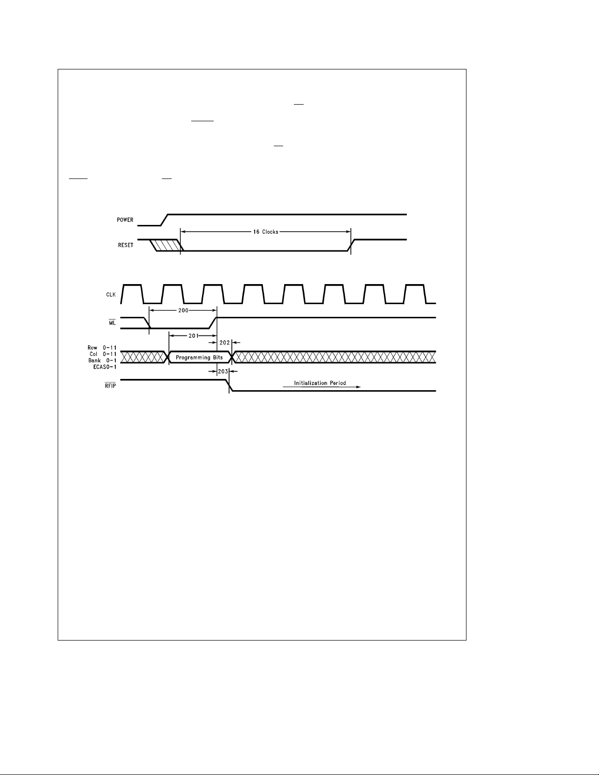
4.0 Programming and Resetting
4.1 RESET
After power up, the DP8440/41 must be reset and programmed before it can be used to access the DRAM. Reset
is accomplished by asserting the input RESET
16 positive edges of CLK after V
the part can be programmed.
stabilizes. After reset,
CC
4.2 PROGRAMMING
Programming is accomplished by presenting a valid programming selection on the row, column, bank selects and
ECAS
inputs and toggling the ML input from low to high.
for at least
When ML
goes high the part is programmed. After the first
programming after a reset the part will enter a 60 ms initialization period. During this period the controller will refresh
the memory, so further DRAM warm up cycles are not necessary. The user can program the part on the fly by pulsing
ML
low and high (provided that no refresh is in progress)
while a valid programming selection is on the address bus.
The part will not enter the initialization period when it is only
re-programmed.
FIGURE 5. Reset
FIGURE 6. Programming
TL/F/11718– 4
TL/F/11718– 5
10

Programming the DP8440/41
4.3 PROGRAMMING SELECTION
RAS LOW AND PRECHARGE TIME
R1 R0
002T
013T
104T
115T
DTACK DURING OPENING ACCESS WILL ASSERT AFTER RAS
R3 R2
001T
012T
103T
114T
DTACK DURING BURST ACCESS WILL ASSERT AFTER CAS
R5 R4
000T
011T
102T
113T
DTACK DURING PAGE ACCESS WILL ASSERT AFTER CAS
R7 R6
000T
011T
102T
113T
PAGE SIZE SELECT
R9 R8
0 0 512
0 1 1024
1 0 2048
1 1 4096
WRAP AROUND SIZE
R11 R10
00 2
01 4
10 8
1116
11
Programming the DP8440/41 (Continued)
4.3 PROGRAMMING SELECTION (Continued)
DIVISOR SELECT
C3 C2 C1 C0
000020
000119
001018
001117
010016
010115
011014
011113
100012
100111
101010
10119
11008
11017
11106
11115
RAS AND CAS CONFIGURATIONS AND REFRESH BEHAVIOR
C5 C4
0 0 All RAS
and all CAS are selected. B0 and B1 are not used. All RAS refresh.
0 1 If C6e0 Non Error B1 B0 is not Used If C6e1 Error B1 B0 is Not Used
1 0 If C6e0 Non Error B1 B0 If C6e1 Error B1 B0
1 1 If C6e0 Non Error B1 B0 is not used. If C6e1 Error B1 B0 is not used.
ERROR SCRUBBING MODE SELECT
C6
Scrubbing Selected. All
CAS Selected. 2-Step
Staggered Refresh. CAS Pairs Selected.
Scrubbing Selected.
All CASs Selected.
4-Step Staggered
Refresh.
Scrubbing. 2-Step
Staggered Refresh.
CAS Pairs Selected. CAS Pairs Selected.
0 Staggered Refresh (Non Error Scrubbing)
1 Error Scrubbing (No CAS
0 RAS0 – 1
1 RAS2 – 3
0 0 RAS0
0 1 RAS1
1 0 RAS2
1 1 RAS3
0 RAS0 – 1 and CAS0,1,4,5
1 RAS2 – 3 and CAS2,3,6,7
-before-RAS and No Staggered Refresh)
Scrubbing Selected.
All RAS Refresh.
Scrubbing Selected.
All RAS Refresh.
CAS Pairs
Selected.
Scrubbing Selected.
All RAS Refresh.
0 RAS0 – 1 and CAS0 – 1, CAS4–5
1 RAS2 – 3 and CAS2 – 3, CAS6–7
0 0 RAS0, CAS0 –4
0 1 RAS1, CAS1 –5
1 0 RAS2, CAS2 –6
1 1 RAS3, CAS3 –7
0 RAS0 – 1 and CAS0,1,4,5
1 RAS2 – 3 and CAS2,3,6,7
12
Programming the DP8440/41 (Continued)
4.3 PROGRAMMING SELECTION (Continued)
ROW ADDRESS HOLD TIME SELECT t
C7
010ns
115ns
PAGMISS INPUT OR OUTPUT SELECT
C8
0 Input
1 Output
CAS PRECHARGE DURING BURST
C9 Read Cycle Write Cycle
0 (/2T1T
11T 2T
REFRESH MODE SELECT
C10
0 RAS
1 CAS
FINE TUNE REFRESH CYCLE
C11
015ms
1 120 ms
COLUMN ADDRESS COUNTER CONTROL SELECT
B0
0 DTACK
1 DTACK
PAGE OR NORMAL MODE SELECT
B1
0 Page Mode
1 Normal Mode
ADDRESS LATCH MODE
ECAS 0
0 Latch Mode
1 Fall Through Mode
BURST REQUEST SELECT (BSTARQ INPUT)
ECAS1
0 Active Low
1 Active High
CAS AND DTACK CLOCK EDGE SELECT
ECAS2
0 Rising Edge
1 Falling Edge
RESERVED
ECAS3
0
1
Only Refresh
-before-RAS Refresh
Falling Edge
Rising Edge
RAH
13
5.0 Accessing Modes
The DP8440/41 are synchronous machines. They allow the
user to access the DRAM in three different ways, Page,
Burst and Normal mode. Every one of these accesses starts
in the same way, this datasheet calls it an Opening Access.
5.1 OPENING ACCESS
Every access starts with ADS
and the address inputs must meet setup timings with respect to the next rising edge of CLK. The DP8440/41
places the row address on the Q outputs and RAS
from the rising edge of CLK that ADS
DP8440/41 guarantees the programmed Row Address Hold
Time, t
place the column address on the Q outputs. After the col-
, before switching the internal multiplexer to
RAH
umn address is valid on the Q outputs, the controller asserts
CAS
. The DRAM controller always guarantees t
DTACK
asserts after RAS according to the programming
selection (R2 –3). If the user programs Latch Mode, through
programming bit ECAS0
column address on the rising edge of ADS
Mode). If not, the controller keeps the latches in a fall
through mode.
and CS asserting. ADS,CS
asserts
is set up to. The
of 0 ns.
ASC
, the DRAM controller latches the
(Normal or Page
5.2 NORMAL MODE
When the controller is programmed in Normal Mode
e
(B1
1), RAS asserts only for the programmed number of
clocks selected by R0 – 1, RAS
Low Time, and automatically
negates from a rising clock edge. To finish the access, CAS
negates from the same clock edge at which DTACK negates. After RAS
negates, the DP8440/41 will guarantee
the programmed number of positive edges of clock for RAS
precharge. RAS will not assert for another access until precharge is met.
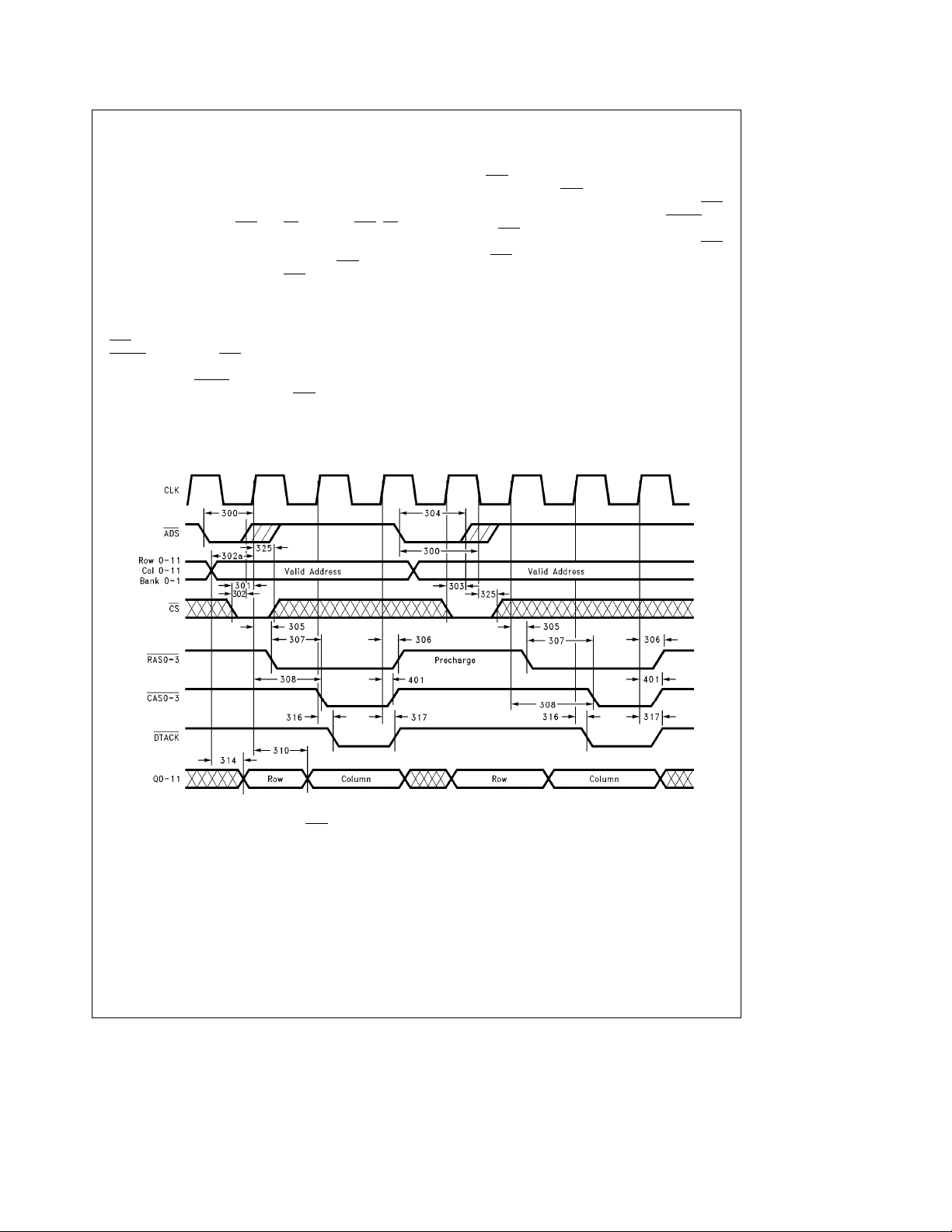
Figure 7
shows an opening access (Normal
Mode) followed by a delayed access due to precharge (accessing the same bank). The second access is delayed by
one clock period to meet precharge time requirements.
FIGURE 7. A Normal Opening Access and Delayed Access
(RAS
Low Time is Programmed for 2 Clocks)
14
TL/F/11718– 6
 Loading...