


NSC DS1489N, DS1489MX, DS1489M, DS1489AN, DS1489AMX Datasheet
...
May 1998
DS1489/DS1489A
Quad Line Receiver
General Description
The DS1489/DS1489A are quad line receivers designed to interface data terminal equipment with data communications equipment. They are constructed on a single monolithic silicon chip. These devices satisfy the specifications of EIA Standard RS-232D. The DS1489/DS1489A meet and exceed the specifications of MC1489/MC1489A and are pin-for-pin replacements.
Features
nFour separate receivers per package
nProgrammable threshold
nBuilt-in input threshold hysteresis
nªFail safeº operating mode: high output for open inputs
nInputs withstand ±30V
Schematic and Connection Diagrams
DS005777-1
(1¤4 of unit shown) DS1489: RF = 10k DS1489A: RF = 2k
Dual-In-Line Package
DS005777-2
Top View
Order Number DS1489M, DS1489N
DS1489AM or DS1489AN
See NS Package Number M14A or N14A
Receiver Line Quad DS1489/DS1489A
© 1998 National Semiconductor Corporation |
DS005777 |
www.national.com |
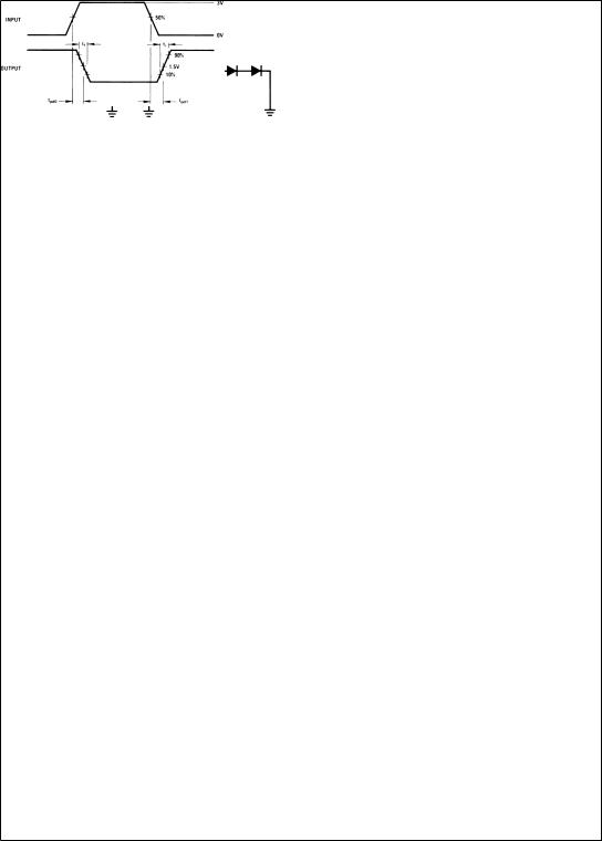
AC Test Circuit and Voltage Waveforms
DS005777-3
DS005777-4
FIGURE 1.
www.national.com |
2 |

Absolute Maximum Ratings (Note 2)
If Military/Aerospace specified devices are required, please contact the National Semiconductor Sales Office/ Distributors for availability and specifications.
Power Supply Voltage |
10V |
Input Voltage Range |
±30V |
Output Load Current |
20 mA |
Power Dissipation (Note 3) |
1W |
Operating Temperature Range |
0ÊC to +75ÊC |
Storage Temperature Range |
−65ÊC to +150ÊC |
Maximum Power Dissipation (Note 1) at 25ÊC |
|
Molded DIP Package |
1207 mW |
SO Package |
1042 mW |
Lead Temperature (Soldering, 4 |
|
sec.) |
260ÊC |
Note 1: Derate molded DIP package 9.7 mW/ÊC above 25ÊC; derate SO package 8.33 mW/ÊC above 25ÊC.
Electrical Characteristics (Notes 3, 4, 5)
DS1489/DS1489A: The following apply for VCC = 5.0V ±1%, 0ÊC £ TA £ +75ÊC unless otherwise specified.
Symbol |
Parameter |
|
Conditions |
|
Min |
Typ |
Max |
Units |
|
|
|
|
|
|
|
|
|
|
|
VTH |
Input High Threshold Voltage |
VOUT £ 0.45V, |
DS1489 |
|
TA = 25ÊC |
1.0 |
1.25 |
1.5 |
V |
|
|
IOUT = 10 mA |
|
|
|
0.9 |
|
1.6 |
V |
|
|
|
DS1489A |
|
TA = 25ÊC |
1.75 |
2.00 |
2.25 |
V |
|
|
|
|
|
|
1.55 |
|
2.40 |
V |
|
|
|
|
|
|
|
|
|
|
VTL |
Input Low Threshold Voltage |
VOUT ³ 2.5V, |
|
|
TA = 25ÊC |
0.75 |
1.00 |
1.25 |
V |
|
|
IOUT = −0.5 mA |
|
|
|
0.65 |
|
1.35 |
V |
IIN |
Input Current |
VIN = +25V |
|
|
|
+3.6 |
+5.6 |
+8.3 |
mA |
|
|
VIN = −25V |
|
|
|
−3.6 |
−5.6 |
−8.3 |
mA |
|
|
VIN = +3V |
|
|
|
+0.43 |
+0.53 |
|
mA |
|
|
VIN = −3V |
|
|
|
−0.43 |
−0.53 |
|
mA |
VOH |
Output High Voltage |
IOUT = −0.5 mA |
V IN = 0.75V |
|
2.6 |
3.8 |
5.0 |
V |
|
|
|
|
Input = Open |
|
2.6 |
3.8 |
5.0 |
V |
|
|
|
|
|
|
|
|
|
|
|
VOL |
Output Low Voltage |
VIN = 3.0V, IOUT = 10 mA |
|
|
0.33 |
0.45 |
V |
||
ISC |
Output Short Circuit Current |
VIN = 0.75V |
|
|
|
|
−3.0 |
|
mA |
ICC |
Supply Current |
VIN = 5.0V |
|
|
|
|
14 |
26 |
mA |
Pd |
Power Dissipation |
VIN = 5.0V |
|
|
|
|
70 |
130 |
mW |
Switching Characteristics
VCC = 5V, TA = 25ÊC
Symbol |
Parameter |
Conditions |
Min |
Typ |
Max |
Units |
tpd1 |
Input to Output ªHighº |
RL = 3.9k, (Figure 1) (AC Test Circuit) |
|
28 |
85 |
ns |
|
Propagation Delay |
|
|
|
|
|
|
|
|
|
|
|
|
tpd0 |
Input to Output ªLowº |
RL = 390W, (Figure 1) (AC Test Circuit) |
|
20 |
50 |
ns |
|
Propagation Delay |
|
|
|
|
|
|
|
|
|
|
|
|
tr |
Output Rise Time |
RL = 3.9k, (Figure 1) (AC Test Circuit) |
|
110 |
175 |
ns |
tf |
Output Fall Time |
RL = 390W, (Figure 1) (AC Test Circuit) |
|
9 |
20 |
ns |
Note 2: ªAbsolute Maximum Ratingsº are those values beyond which the safety of the device cannot be guaranteed. Except for ªOperating Temperature Rangeº they are not meant to imply that the devices should be operated at these limits. The table of ªElectrical Characteristicsº provides conditions for actual eviced operation.
Note 3: Unless otherwise specified min/max limits apply across the 0ÊC to +75ÊC temperature range for the DS1489 and DS1489A.
Note 4: All currents into device pins shown as positive, out of device pins as negative, all voltages referenced to ground unless otherwise noted. All values shown as max or min on absolute value basis.
Note 5: These specifications apply for response control pin = open.
3 |
www.national.com |
 Loading...