


LM1117MPX-5.0
NSC LM1117MPX-5.0, LM1117T-ADJ, LM1117T-5.0, LM1117T-3.3, LM1117T-2.85 Datasheet
...
LM1117
800mA Low-Dropout Linear Regulator
General Description
The LM1117 is a series of low dropout voltage regulators
with a dropout of 1.2V at 800mA of load current. It has the
same pin-out as National Semiconductor’s industry standard
LM317.
The LM1117 is available in an adjustable version, which can
set the output voltage from 1.25V to 13.8V with only two external resistors. In addition, it is also available in five fixed
voltages, 1.8V, 2.5V, 2.85V, 3.3V, and 5V.
The LM1117 offers current limiting and thermal shutdown. Its
circuit includes a zener trimmed bandgap reference to assure output voltage accuracy to within
±
1%.
The LM1117 series is available in SOT-223, TO-220, and
TO-252 D-PAK packages. A minimum of 10µF tantalum capacitor is required at the output to improve the transient response and stability.
Features
n Available in 1.8V, 2.5V, 2.85V, 3.3V, 5V, and Adjustable
Versions
n Space Saving SOT-223 Package
n Current Limiting and Thermal Protection
n Output Current 800mA
n Temperature Range 0˚C to 125˚C
n Line Regulation 0.2%(Max)
n Load Regulation 0.4%(Max)
Applications
n 2.85V Model for SCSI-2 Active Termination
n Post Regulator for Switching DC/DC Converter
n High Efficiency Linear Regulators
n Battery Charger
n Battery Powered Instrumentation
Typical Application
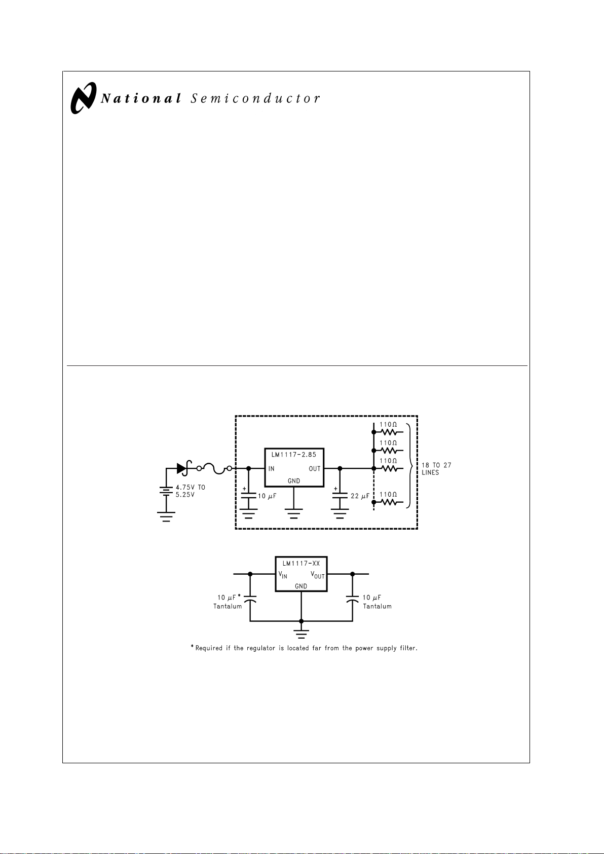
Active Terminator for SCSI-2 Bus
DS100919-5
Fixed Output Regulator
DS100919-28
February 2000
LM1117 800mA Low-Dropout Linear Regulator
© 2000 National Semiconductor Corporation DS100919 www.national.com
Ordering Information
Package
Temperature Range
Packaging Marking Transport Media NSC Drawing
0˚C to +125˚C
3-lead SOT-223 LM1117MPX-ADJ N03A Tape and Reel MA04A
LM1117MPX-1.8 N12A Tape and Reel
* LM1117MPX-2.5 N13A Tape and Reel
LM1117MPX-2.85 N04A Tape and Reel
LM1117MPX-3.3 N05A Tape and Reel
LM1117MPX-5.0 N06A Tape and Reel
3-lead TO-220 LM1117T-ADJ LM1117T-ADJ Rails T03B
LM1117T-2.85 LM1117T-2.85 Rails
LM1117T-3.3 LM1117T-3.3 Rails
LM1117T-5.0 LM1117T-5.0 Rails
3-lead TO-252 LM1117DTX-ADJ LM1117DT-ADJ Tape and Reel TD03B
LM1117DTX-1.8 LM1117DT-1.8 Tape and Reel
* LM1117DTX-2.5 LM1117DT-2.5 Tape and Reel
LM1117DTX-2.85 LM1117DT-2.85 Tape and Reel
LM1117DTX-3.3 LM1117DT-3.3 Tape and Reel
LM1117DTX-5.0 LM1117DT-5.0 Tape and Reel
Note:*Contact factory for availability.
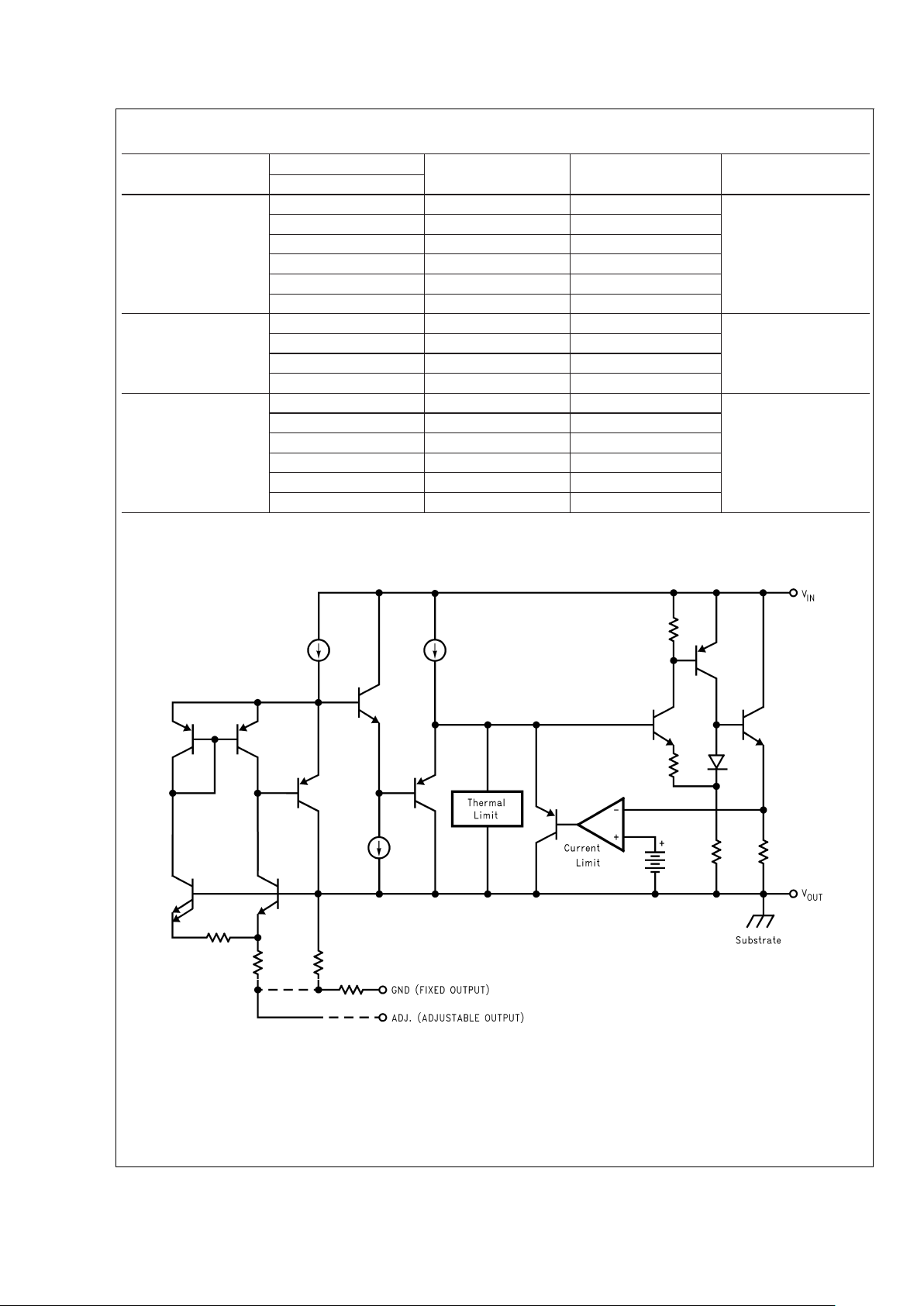
Block Diagram
DS100919-1
LM1117
www.national.com 2
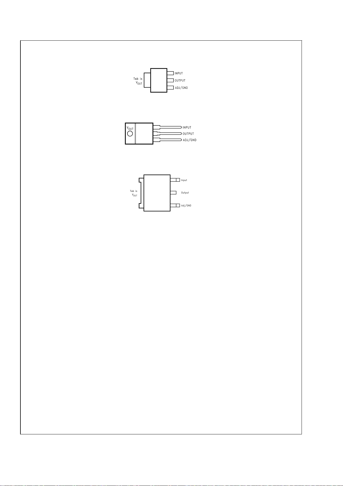
Connection Diagrams
SOT-223
DS100919-4
Top View
TO-220
DS100919-2
Top View
TO-252
DS100919-38
Top View
LM1117
www.national.com3
Absolute Maximum Ratings (Note 1)
If Military/Aerospace specified devices are required,
please contact the NationalSemiconductor Sales Office/
Distributors for availability and specifications.
Maximum Input Voltage (V
IN
to GND)
LM1117-ADJ, LM1117-1.8,
LM1117-2.5, LM1117-3.3,
LM1117-5.0 20V
Power Dissipation (Note 2) Internally Limited
Junction Temperature (T
J
)
(Note 2)
150˚C
Storage Temperature Range -65˚C to 150˚C
Lead Temperature
TO-220 (T) Package 260˚C, 10 sec
SOT-223 (IMP) Package 260˚C, 4 sec
ESD Tolerance (Note 3) 2000V
Operating Ratings (Note 1)
Input Voltage (V
IN
to GND)
LM1117-ADJ, LM1117-1.8,
LM1117-2.5, LM1117-3.3,
LM1117-5.0
15V
LM1117-2.85 10V
Junction Temperature Range
(T
J
)(Note 2)
0˚C to 125˚C
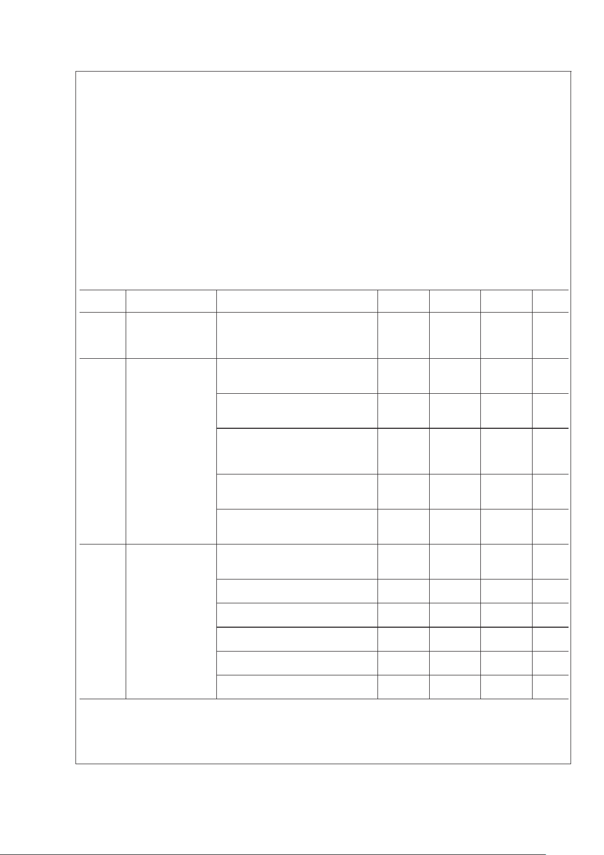
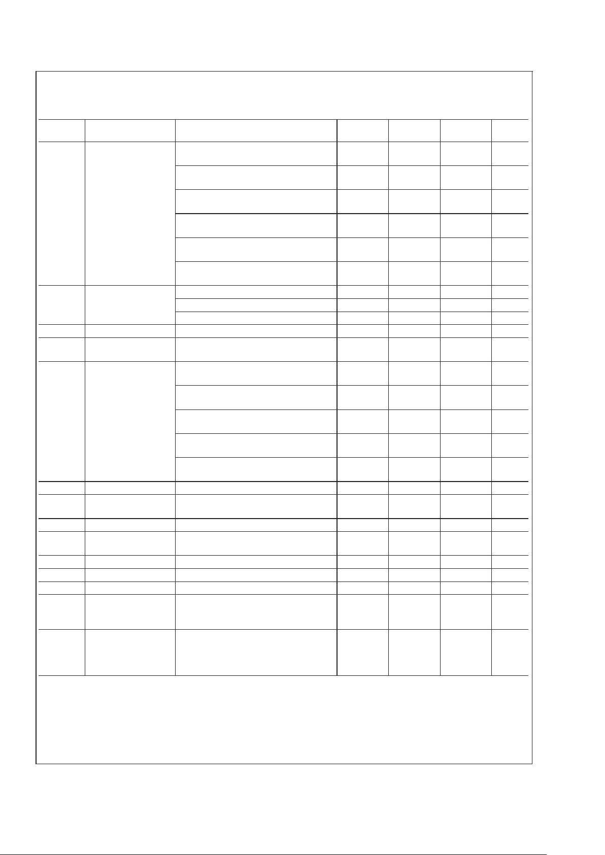
Electrical Characteristics
Typicals and limits appearing in normal type apply for TJ= 25˚C. Limits appearing in Boldface type apply over the entire junction temperature range for operation, 0˚C to 125˚C.
Symbol Parameter Conditions
Min
(Note 5)
Typ
(Note 4)
Max
(Note 5)
Units
V
REF
Reference Voltage LM1117-ADJ
I
OUT
= 10mA, VIN-V
OUT
= 2V, TJ= 25˚C
10mA ≤ I
OUT
≤ 800mA, 1.4V ≤ VIN-V
OUT
≤ 10V
1.238
1.225
1.250
1.250
1.262
1.270
V
V
V
OUT
Output Voltage LM1117-1.8
I
OUT
= 10mA, VIN= 3.8V, TJ= 25˚C
0 ≤ I
OUT
≤ 800mA, 3.2V ≤ VIN≤ 10V
1.782
1.746
1.800
1.800
1.818
1.854
V
V
LM1117-2.5
I
OUT
= 10mA, VIN= 4.5V, TJ= 25˚C
0 ≤ I
OUT
≤ 800mA, 3.9V ≤ VIN≤ 10V
2.475
2.450
2.500
2.500
2.525
2.550
V
V
LM1117-2.85
I
OUT
= 10mA, VIN= 4.85V, TJ= 25˚C
0 ≤ I
OUT
≤ 800mA, 4.25V ≤ VIN≤ 10V
0 ≤ I
OUT
≤ 500mA, VIN= 4.10V
2.820
2.790
2.790
2.850
2.850
2.850
2.880
2.910
2.910
V
V
V
LM1117-3.3
I
OUT
= 10mA, VIN=5VTJ= 25˚C
0 ≤ I
OUT
≤ 800mA, 4.75V≤ VIN≤ 10V
3.267
3.235
3.300
3.300
3.333
3.365
V
V
LM1117-5.0
I
OUT
= 10mA, VIN= 7V, TJ= 25˚C
0 ≤ I
OUT
≤ 800mA, 6.5V ≤ VIN≤ 12V
4.950
4.900
5.000
5.000
5.050
5.100
V
V
∆V
OUT
Line Regulation
(Note 6)
LM1117-ADJ
I
OUT
= 10mA, 1.5V ≤ VIN-V
OUT
≤
13.75V
0.035 0.2
%
LM1117-1.8
I
OUT
= 0mA, 3.2V ≤ VIN≤ 10V
1 6 mV
LM1117-2.5
I
OUT
= 0mA, 3.9V ≤ VIN≤ 10V
1 6 mV
LM1117-2.85
I
OUT
= 0mA, 4.25V ≤ VIN≤ 10V 1 6 mV
LM1117-3.3
I
OUT
= 0mA, 4.75V ≤ VIN≤ 15V 1 6 mV
LM1117-5.0
I
OUT
= 0mA, 6.5V ≤ VIN≤ 15V 1 10 mV
LM1117
www.national.com 4
Electrical Characteristics (Continued)
Typicals and limits appearing in normal type apply for TJ= 25˚C. Limits appearing in Boldface type apply over the entire junction temperature range for operation, 0˚C to 125˚C.
Symbol Parameter Conditions
Min
(Note 5)
Typ
(Note 4)
Max
(Note 5)
Units
∆V
OUT
Load Regulation
(Note 6)
LM1117-ADJ
V
IN-VOUT
= 3V, 10 ≤ I
OUT
≤ 800mA 0.2 0.4
%
LM1117-1.8
V
IN
= 3.2V, 0 ≤ I
OUT
≤ 800mA
1 10 mV
LM1117-2.5
V
IN
= 3.9V, 0 ≤ I
OUT
≤ 800mA
1 10 mV
LM1117-2.85
V
IN
= 4.25V, 0 ≤ I
OUT
≤ 800mA 1 10 mV
LM1117-3.3
V
IN
= 4.75V, 0 ≤ I
OUT
≤ 800mA 1 10 mV
LM1117-5.0
V
IN
= 6.5V, 0 ≤ I
OUT
≤ 800mA 1 15 mV
V
IN-VOUT
Dropout Voltage
(Note 7)
I
OUT
= 100mA 1.10 1.20 V
I
OUT
= 500mA 1.15 1.25 V
I
OUT
= 800mA 1.20 1.30 V
I
LIMIT
Current Limit VIN-V
OUT
= 5V, TJ= 25˚C 800 1200 1500 mA
Minimum Load
Current (Note 8)
LM1117-ADJ
V
IN
= 15V 1.7 5 mA
Quiescent Current LM1117-1.8
V
IN
≤ 15V
5 10 mA
LM1117-2.5
V
IN
≤ 15V
5 10 mA
LM1117-2.85
V
IN
≤ 10V 5 10 mA
LM1117-3.3
V
IN
≤ 15V 5 10 mA
LM1117-5.0
V
IN
≤ 15V 5 10 mA
Thermal Regulation T
A
= 25˚C, 30ms Pulse 0.01 0.1
%
/W
Ripple Regulation f
RIPPLE
=1 20Hz, VIN-V
OUT
=3V
V
RIPPLE
=1V
PP
60 75 dB
Adjust Pin Current 60 120 µA
Adjust Pin Current
Change
10 ≤ I
OUT
≤ 800mA,
1.4V ≤ V
IN-VOUT
≤ 10V 0.2 5 µA
Temperature Stability 0.5
%
Long Term Stability T
A
= 125˚C, 1000Hrs 0.3
%
RMS Output Noise (%of V
OUT
), 10Hz ≤ f ≤10kHz 0.003
%
Thermal Resistance
Junction-to-Case
3-Lead SOT-223
3-Lead TO-220
3-Lead TO-252
15.0
3.0
10
˚C/W
˚C/W
˚C/W
Thermal Resistance
Junction-to-Ambient
(No heat sink;
No air flow)
3-Lead SOT-223
3-Lead TO-220
3-Lead TO-252 (Note 9)
136
79
92
˚C/W
˚C/W
˚C/W
Note 1: Absolute Maximum Ratings indicatelimits beyond which damage to the device may occur. Operating Ratings indicate conditions for which the device is intended to be functional, but specific performance is not guaranteed. For guaranteed specifications and the test conditions, see the Electrical Characteristics.
Note 2: The maximum power dissipation is a function of T
J(max)
, θJA, and TA. The maximum allowable power dissipation at any ambient temperature is
P
D
=(T
J(max)–TA
)/θJA. All numbers apply for packages soldered directly into a PC board.
Note 3: For testing purposes, ESD was applied using human body model, 1.5kΩ in series with 100pF.
Note 4: Typical Values represent the most likely parametric norm.
Note 5: All limits are guaranteed by testing or statistical analysis.
Note 6: Load and line regulation are measured at constant junction room temperature.
LM1117
www.national.com5

Electrical Characteristics (Continued)
Note 7: The dropout voltage is the input/output differential at which the circuit ceases to regulate against further reduction in input voltage. It is measured when the
output voltage has dropped 100mV from the nominal value obtained at V
IN=VOUT
+1.5V.
Note 8: The minimum output current required to maintain regulation.
Note 9: Minimum pad size of 0.038in
2
LM1117
www.national.com 6
 Loading...