


NSC COP8CCR9LVA8, COP8CCR9LVA7, COP8CCR9KMT7, COP8CCR9IMT7, COP8CCR9HVA7 Datasheet
...August 2003
COP8CBR9/COP8CCR9/COP8CDR9
8-Bit CMOS Flash Microcontroller with 32k Memory, Virtual EEPROM, 10-Bit A/D and Brownout
1.0 General Description
The COP8CBR/CCR/CDR9 Flash microcontrollers are highly integrated COP8™ Feature core devices, with 32k Flash memory and advanced features including Virtual EEPROM, A/D, High Speed Timers, USART, and Brownout Reset. This single-chip CMOS device is suited for applica-
Device included in this datasheet:
tions requiring a full featured, in-system reprogrammable controller with large memory and low EMI. The same device is used for development, pre-production and volume production with a range of COP8 software and hardware development tools.
|
Flash Program |
RAM |
Brownout |
I/O |
|
|
|
Device |
Memory |
Packages |
Temperature |
||||
(bytes) |
Voltage |
Pins |
|||||
|
(bytes) |
|
|
||||
|
|
|
|
|
|
||
|
|
|
|
|
|
|
|
|
|
|
|
37,39,49, |
44 LLP, |
|
|
COP8CBR9 |
32k |
1k |
2.7V to 2.9V |
44/68 PLCC, |
−40˚C to +85˚C |
||
59 |
|||||||
|
|
|
|
48/56 TSSOP |
|
||
|
|
|
|
|
|
||
|
|
|
|
|
|
|
|
|
|
|
|
37,39,49, |
44 LLP, |
−40˚C to +85˚C |
|
COP8CCR9 |
32k |
1k |
4.17V to 4.5V |
44/68 PLCC, |
|||
59 |
−40˚C to +125˚C |
||||||
|
|
|
|
48/56 TSSOP |
|||
|
|
|
|
|
|
||
|
|
|
|
|
|
|
|
|
|
|
|
37,39,49, |
44 LLP, |
−40˚C to +85˚C |
|
COP8CDR9 |
32k |
1k |
No Brownout |
44/68 PLCC, |
|||
59 |
−40˚C to +125˚C |
||||||
|
|
|
|
48/56 TSSOP |
|||
|
|
|
|
|
|
||
|
|
|
|
|
|
|
2.0 Features
KEY FEATURES
n32 kbytes Flash Program Memory with Security Feature
nVirtual EEPROM using Flash Program Memory
n1 kbyte volatile RAM
n10-bit Successive Approximation Analog to Digital Converter (up to 16 channels)
n100% Precise Analog Emulation
nUSART with onchip baud generator
n2.7V – 5.5V In-System Programmability of Flash
nHigh endurance -100k Read/Write Cycles
nSuperior Data Retention - 100 years
nDual Clock Operation with HALT/IDLE Power Save Modes
nThree 16-bit timers:
—Timers T2 and T3 can operate at high speed (50 ns resolution)
—Processor Independent PWM mode
—External Event counter mode
—Input Capture mode
nBrown-out Reset (COP8CBR9/CCR9)
OTHER FEATURES
nSingle supply operation:
—2.7V–5.5V (−40˚C to +85˚C)
—4.5V–5.5V (−40˚C to +125˚C)
nQuiet Design (low radiated emissions)
nMulti-Input Wake-up with optional interrupts
nMICROWIRE/PLUS (Serial Peripheral Interface Compatible)
nClock Doubler for 20 MHz operation from 10 MHz Oscillator, with 0.5 µs Instruction Cycle
nThirteen multi-source vectored interrupts servicing:
—External Interrupt
—USART (2)
—Idle Timer T0
—Three Timers (each with 2 interrupts)
—MICROWIRE/PLUS Serial peripheral interface
—Multi-Input Wake-up
—Software Trap
nIdle Timer with programmable interrupt interval
n8-bit Stack Pointer SP (stack in RAM)
nTwo 8-bit Register Indirect Data Memory Pointers
nTrue bit manipulation
nWATCHDOG and Clock Monitor logic
nSoftware selectable I/O options
—TRI-STATE® Output/High Impedance Input
—Push-Pull Output
—Weak Pull Up Input
nSchmitt trigger inputs on I/O ports
nHigh Current I/Os
nTemperature range: –40˚C to +85˚C and –40˚C to +125˚C (COP8CCR9/CDR9)
nPackaging: 44 and 68 PLCC, 44 LLP, 48 and 56 TSSOP
nTrue In-System, real time emulation and debug tools available
COP8™ is a trademark of National Semiconductor Corporation.
Memory, 32k with Microcontroller Based Flash CMOS Bit-8 COP8CBR9/COP8CCR9/COP8CDR9
Brownout and A/D Bit-10 EEPROM, Virtual
© 2003 National Semiconductor Corporation |
DS101374 |
www.national.com |

COP8CBR9/COP8CCR9/COP8CDR9
3.0 Block Diagram
|
|
|
|
|
|
10137401 |
4.0 Ordering Information |
|
|
|
|
|
|
|
|
Part Numbering Scheme |
|
|
||
|
|
|
|
|
|
|
COP8 |
CB |
R |
9 |
H |
VA |
8 |
|
|
|
|
|
|
|
|
Family and |
Program |
Program |
|
Package |
|
|
Feature Set |
Memory |
Memory |
No. Of Pins |
Temperature |
|
|
Type |
|||||
|
Indicator |
Size |
Type |
|
|
|
|
|
|
|
|||
|
|
|
|
|
|
|
|
CB = Low Brownout Voltage |
R = 32k |
9 = Flash |
H = 44 Pin |
LQ = LLP |
7 = -40 to +125˚C |
|
CC = High Brownout Voltage |
|
|
I = 48 Pin |
MT = TSSOP |
8 = -40 to +85˚C |
|
CD = No Brownout |
|
|
k = 56 Pin |
VA = PLCC |
|
|
|
|
|
L = 68 Pin |
|
|
|
|
|
|
|
|
|
www.national.com |
2 |

Table of Contents |
|
1.0 General Description ..................................................................................................................................... |
1 |
2.0 Features ....................................................................................................................................................... |
1 |
3.0 Block Diagram .............................................................................................................................................. |
2 |
4.0 Ordering Information .................................................................................................................................... |
2 |
5.0 Connection Diagrams ................................................................................................................................... |
6 |
6.0 Architectural Overview ............................................................................................................................... |
10 |
6.1 EMI REDUCTION .................................................................................................................................... |
10 |
6.2 IN-SYSTEM PROGRAMMING AND VIRTUAL EEPROM ...................................................................... |
10 |
6.3 DUAL CLOCK AND CLOCK DOUBLER ................................................................................................. |
10 |
6.4 TRUE IN-SYSTEM EMULATION ............................................................................................................ |
10 |
6.5 ARCHITECTURE ................................................................................................................................... |
10 |
6.6 INSTRUCTION SET ............................................................................................................................... |
10 |
6.6.1 Key Instruction Set Features ............................................................................................................. |
10 |
6.6.2 Single Byte/Single Cycle Code Execution ....................................................................................... |
10 |
6.6.3 Many Single-Byte, Multi-Function Instructions .................................................................................. |
10 |
6.6.4 Bit-Level Control ................................................................................................................................ |
11 |
6.6.5 Register Set ....................................................................................................................................... |
11 |
6.7 PACKAGING/PIN EFFICIENCY .............................................................................................................. |
11 |
7.0 Absolute Maximum Ratings ....................................................................................................................... |
12 |
8.0 Electrical Characteristics ............................................................................................................................ |
12 |
9.0 Pin Descriptions ......................................................................................................................................... |
18 |
9.1 EMULATION CONNECTION ................................................................................................................... |
20 |
10.0 Functional Description .............................................................................................................................. |
20 |
10.1 CPU REGISTERS ................................................................................................................................. |
20 |
10.2 PROGRAM MEMORY ........................................................................................................................... |
20 |
10.3 DATA MEMORY .................................................................................................................................... |
20 |
10.4 DATA MEMORY SEGMENT RAM EXTENSION .................................................................................. |
21 |
10.4.1 Virtual EEPROM .............................................................................................................................. |
22 |
10.5 OPTION REGISTER ............................................................................................................................. |
22 |
10.6 SECURITY ............................................................................................................................................ |
23 |
10.7 RESET ................................................................................................................................................... |
23 |
10.7.1 External Reset ................................................................................................................................. |
24 |
10.7.2 On-Chip Brownout Reset ................................................................................................................. |
24 |
10.8 OSCILLATOR CIRCUITS ...................................................................................................................... |
26 |
10.8.1 Oscillator .......................................................................................................................................... |
26 |
................................................................................................................................................................... |
0 |
10.8.2 Clock Doubler .................................................................................................................................. |
27 |
10.9 CONTROL REGISTERS ....................................................................................................................... |
27 |
10.9.1 CNTRL Register (Address X'00EE) ................................................................................................. |
27 |
10.9.2 PSW Register (Address X'00EF) ..................................................................................................... |
27 |
10.9.3 ICNTRL Register (Address X'00E8) ................................................................................................ |
27 |
10.9.4 T2CNTRL Register (Address X'00C6) ............................................................................................. |
27 |
10.9.5 T3CNTRL Register (Address X'00B6) ............................................................................................. |
27 |
10.9.6 HSTCR Register (Address X'00AF) ................................................................................................ |
28 |
10.9.7 ITMR Register (Address X'00CF) .................................................................................................... |
28 |
10.9.8 ENAD Register (Address X'00CB) .................................................................................................. |
28 |
11.0 In-System Programming ........................................................................................................................... |
28 |
11.1 INTRODUCTION ................................................................................................................................... |
28 |
11.2 FUNCTIONAL DESCRIPTION .............................................................................................................. |
28 |
11.3 REGISTERS .......................................................................................................................................... |
29 |
11.3.1 ISP Address Registers ..................................................................................................................... |
29 |
11.3.2 ISP Read Data Register .................................................................................................................. |
29 |
11.3.3 ISP Write Data Register ................................................................................................................... |
29 |
11.3.4 ISP Write Timing Register ................................................................................................................ |
29 |
11.4 MANEUVERING BACK AND FORTH BETWEEN FLASH MEMORY AND BOOT ROM ..................... |
30 |
11.5 FORCED EXECUTION FROM BOOT ROM ......................................................................................... |
30 |
11.6 RETURN TO FLASH MEMORY WITHOUT HARDWARE RESET ....................................................... |
31 |
11.7 MICROWIRE/PLUS ISP ........................................................................................................................ |
31 |
11.8 USER ISP AND VIRTUAL E2 ................................................................................................................ |
32 |
11.9 RESTRICTIONS ON SOFTWARE WHEN CALLING ISP ROUTINES IN BOOT ROM ....................... |
34 |
11.10 FLASH MEMORY DURABILITY CONSIDERATIONS ........................................................................ |
34 |
12.0 Timers ....................................................................................................................................................... |
35 |
COP8CBR9/COP8CCR9/COP8CDR9
3 |
www.national.com |

COP8CBR9/COP8CCR9/COP8CDR9
|
Table of Contents (Continued) |
|
12.1 |
TIMER T0 (IDLE TIMER) ...................................................................................................................... |
35 |
12.1.1 ITMR Register .................................................................................................................................. |
36 |
|
12.2 |
TIMER T1, TIMER T2, AND TIMER T3 ................................................................................................ |
36 |
12.2.1 Timer Operating Speeds .................................................................................................................. |
36 |
|
12.2.2 Mode 1. Processor Independent PWM Mode ................................................................................. |
36 |
|
12.2.3 Mode 2. External Event Counter Mode ........................................................................................... |
37 |
|
12.2.4 Mode 3. Input Capture Mode .......................................................................................................... |
37 |
|
12.3 |
TIMER CONTROL FLAGS .................................................................................................................... |
38 |
13.0 Power Saving Features ............................................................................................................................ |
38 |
|
13.1 |
POWER SAVE MODE CONTROL REGISTER .................................................................................... |
39 |
13.2 |
OSCILLATOR STABILIZATION ............................................................................................................. |
40 |
13.3 |
HIGH SPEED MODE OPERATION ...................................................................................................... |
40 |
13.3.1 High Speed Halt Mode .................................................................................................................... |
40 |
|
13.3.1.1 Entering The High Speed Halt Mode ......................................................................................... |
40 |
|
13.3.1.2 Exiting The High Speed Halt Mode ........................................................................................... |
40 |
|
13.3.1.3 HALT Exit Using Reset .............................................................................................................. |
40 |
|
13.3.1.4 HALT Exit Using Multi-Input Wake-up ....................................................................................... |
40 |
|
13.3.1.5 Options ....................................................................................................................................... |
41 |
|
13.3.2 High Speed Idle Mode ..................................................................................................................... |
41 |
|
13.4 |
DUAL CLOCK MODE OPERATION ...................................................................................................... |
42 |
13.4.1 Dual Clock HALT Mode ................................................................................................................... |
42 |
|
13.4.1.1 Entering The Dual Clock Halt Mode .......................................................................................... |
42 |
|
13.4.1.2 Exiting The Dual Clock Halt Mode ............................................................................................. |
42 |
|
13.4.1.3 HALT Exit Using Reset .............................................................................................................. |
42 |
|
13.4.1.4 HALT Exit Using Multi-Input Wake-up ....................................................................................... |
42 |
|
13.4.1.5 Options ....................................................................................................................................... |
42 |
|
13.4.2 Dual Clock Idle Mode ...................................................................................................................... |
42 |
|
13.5 |
LOW SPEED MODE OPERATION ....................................................................................................... |
43 |
13.5.1 Low Speed HALT Mode ................................................................................................................... |
43 |
|
13.5.1.1 Entering The Low Speed Halt Mode ......................................................................................... |
43 |
|
13.5.1.2 Exiting The Low Speed Halt Mode ............................................................................................ |
43 |
|
13.5.1.3 HALT Exit Using Reset .............................................................................................................. |
43 |
|
13.5.1.4 HALT Exit Using Multi-Input Wake-up ....................................................................................... |
43 |
|
13.5.1.5 Options ....................................................................................................................................... |
43 |
|
13.5.2 Low Speed Idle Mode ...................................................................................................................... |
44 |
|
13.6 |
MULTI-INPUT WAKE-UP ...................................................................................................................... |
45 |
14.0 USART ..................................................................................................................................................... |
45 |
|
14.1 |
USART CONTROL AND STATUS REGISTERS ................................................................................... |
46 |
14.2 |
DESCRIPTION OF USART REGISTER BITS ...................................................................................... |
46 |
14.3 ASSOCIATED I/O PINS ........................................................................................................................ |
47 |
|
14.4 |
USART OPERATION ............................................................................................................................ |
48 |
14.4.1 Asynchronous Mode ........................................................................................................................ |
48 |
|
14.4.2 Synchronous Mode .......................................................................................................................... |
48 |
|
14.5 |
FRAMING FORMATS ............................................................................................................................ |
48 |
14.6 |
USART INTERRUPTS .......................................................................................................................... |
49 |
14.7 |
BAUD CLOCK GENERATION .............................................................................................................. |
49 |
14.8 |
EFFECT OF HALT/IDLE ....................................................................................................................... |
51 |
14.9 |
DIAGNOSTIC ........................................................................................................................................ |
51 |
14.10 ATTENTION MODE ............................................................................................................................. |
51 |
|
14.11 BREAK GENERATION ........................................................................................................................ |
51 |
|
15.0 A/D Converter ........................................................................................................................................... |
51 |
|
15.1 |
OPERATING MODES ........................................................................................................................... |
52 |
15.1.1 A/D Control Register ........................................................................................................................ |
52 |
|
15.1.1.1 Channel Select ........................................................................................................................... |
52 |
|
15.1.1.2 Multiplexor Output Select ........................................................................................................... |
53 |
|
15.1.1.3 Mode Select ............................................................................................................................... |
54 |
|
15.1.1.4 Prescaler Select ......................................................................................................................... |
54 |
|
15.1.1.5 Busy Bit ...................................................................................................................................... |
54 |
|
15.1.2 A/D Result Registers ....................................................................................................................... |
54 |
|
15.2 A/D OPERATION ................................................................................................................................... |
55 |
|
15.2.1 Prescaler .......................................................................................................................................... |
55 |
|
www.national.com |
4 |

|
Table of Contents (Continued) |
|
15.3 ANALOG INPUT AND SOURCE RESISTANCE CONSIDERATIONS .................................................. |
55 |
|
16.0 Interrupts .................................................................................................................................................. |
56 |
|
16.1 |
INTRODUCTION ................................................................................................................................... |
56 |
16.2 |
MASKABLE INTERRUPTS ................................................................................................................... |
56 |
16.3 |
VIS INSTRUCTION ............................................................................................................................... |
57 |
16.3.1 VIS Execution .................................................................................................................................. |
58 |
|
16.4 |
NON-MASKABLE INTERRUPT ............................................................................................................ |
59 |
16.4.1 Pending Flag .................................................................................................................................... |
59 |
|
16.4.2 Software Trap .................................................................................................................................. |
59 |
|
16.4.2.1 Programming Example: External Interrupt ................................................................................. |
60 |
|
16.5 |
PORT L INTERRUPTS .......................................................................................................................... |
61 |
16.6 |
INTERRUPT SUMMARY ....................................................................................................................... |
61 |
17.0 WATCHDOG/Clock Monitor ..................................................................................................................... |
61 |
|
17.1 |
CLOCK MONITOR ................................................................................................................................ |
62 |
17.2 |
WATCHDOG/CLOCK MONITOR OPERATION .................................................................................... |
62 |
17.3 WATCHDOG AND CLOCK MONITOR SUMMARY .............................................................................. |
63 |
|
17.4 |
DETECTION OF ILLEGAL CONDITIONS ............................................................................................ |
63 |
18.0 MICROWIRE/PLUS .................................................................................................................................. |
63 |
|
18.1 |
MICROWIRE/PLUS OPERATION ......................................................................................................... |
64 |
18.1.1 MICROWIRE/PLUS Master Mode Operation .................................................................................. |
64 |
|
18.1.2 MICROWIRE/PLUS Slave Mode Operation .................................................................................... |
64 |
|
18.1.2.1 Alternate SK Phase Operation and SK Idle Polarity ................................................................. |
65 |
|
19.0 Memory Map ............................................................................................................................................ |
66 |
|
20.0 Instruction Set .......................................................................................................................................... |
67 |
|
20.1 |
INTRODUCTION ................................................................................................................................... |
67 |
20.2 |
INSTRUCTION FEATURES .................................................................................................................. |
67 |
20.3 ADDRESSING MODES ......................................................................................................................... |
68 |
|
20.3.1 Operand Addressing Modes ............................................................................................................ |
68 |
|
20.3.2 Tranfer-of-Control Addressing Modes .............................................................................................. |
69 |
|
20.4 |
INSTRUCTION TYPES ......................................................................................................................... |
69 |
20.4.1 Arithmetic Instructions ...................................................................................................................... |
70 |
|
20.4.2 Transfer-of-Control Instructions ....................................................................................................... |
70 |
|
20.4.3 Load and Exchange Instructions ..................................................................................................... |
70 |
|
20.4.4 Logical Instructions .......................................................................................................................... |
70 |
|
20.4.5 Accumulator Bit Manipulation Instructions ....................................................................................... |
70 |
|
20.4.6 Stack Control Instructions ................................................................................................................ |
70 |
|
20.4.7 Memory Bit Manipulation Instructions ............................................................................................. |
70 |
|
20.4.8 Conditional Instructions ................................................................................................................... |
70 |
|
20.4.9 No-Operation Instruction .................................................................................................................. |
70 |
|
20.5 |
REGISTER AND SYMBOL DEFINITION .............................................................................................. |
70 |
20.6 |
INSTRUCTION SET SUMMARY .......................................................................................................... |
72 |
20.7 |
INSTRUCTION EXECUTION TIME ...................................................................................................... |
73 |
21.0 Development Support .............................................................................................................................. |
76 |
|
21.1 TOOLS ORDERING NUMBERS FOR THE COP8 FLASH FAMILY DEVICES ................................... |
76 |
|
21.2 |
COP8 TOOLS OVERVIEW ................................................................................................................... |
78 |
21.3 |
WHERE TO GET TOOLS ..................................................................................................................... |
79 |
22.0 Revision History ....................................................................................................................................... |
80 |
|
23.0 Physical Dimensions ................................................................................................................................ |
83 |
|
COP8CBR9/COP8CCR9/COP8CDR9
5 |
www.national.com |
COP8CBR9/COP8CCR9/COP8CDR9
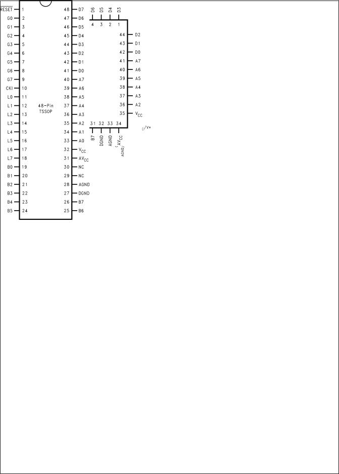
5.0 Connection Diagrams
10137402
Top View
Plastic Chip Package
See NS Package Number V68A
10137455
Top View
LLP Package
See NS Package Number LQA44A
10137403
Top View
Plastic Chip Package
See NS Package Number V44A
10137456
Top View
TSSOP Package
See NS Package Number MTD48
www.national.com |
6 |
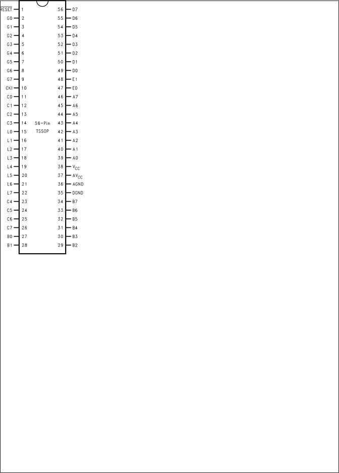
5.0 Connection Diagrams (Continued)
10137457
Top View
TSSOP Package
See NS Package Number MTD56
COP8CBR9/COP8CCR9/COP8CDR9
7 |
www.national.com |

COP8CBR9/COP8CCR9/COP8CDR9
5.0 Connection Diagrams |
(Continued) |
|
|
|
|
|
|||
|
|
|
TABLE 1. Pinouts for All Packages |
|
|
|
|||
|
|
|
|
|
|
|
|
|
|
|
|
|
In System |
|
44-Pin |
48-Pin |
56-Pin |
68-Pin |
|
Port |
Type |
Alt. Fun |
Emulation |
44-Pin LLP |
|||||
PLCC |
TSSOP |
TSSOP |
PLCC |
||||||
|
|
|
Mode |
|
|||||
|
|
|
|
|
|
|
|
||
|
|
|
|
|
|
|
|
|
|
L0 |
I/O |
MIWU or Low Speed OSC In |
|
16 |
11 |
11 |
15 |
22 |
|
L1 |
I/O |
MIWU or CKX or Low Speed |
|
17 |
12 |
12 |
16 |
23 |
|
|
|
OSC Out |
|
|
|
|
|
|
|
L2 |
I/O |
MIWU or TDX |
|
18 |
13 |
13 |
17 |
24 |
|
L3 |
I/O |
MIWU or RDX |
|
19 |
14 |
14 |
18 |
25 |
|
L4 |
I/O |
MIWU or T2A |
|
20 |
15 |
15 |
19 |
26 |
|
L5 |
I/O |
MIWU or T2B |
|
21 |
16 |
16 |
20 |
27 |
|
L6 |
I/O |
MIWU or T3A |
|
22 |
17 |
17 |
21 |
28 |
|
L7 |
I/O |
MIWU or T3B |
|
23 |
18 |
18 |
22 |
29 |
|
|
|
|
|
|
|
|
|
|
|
G0 |
I/O |
INT |
Input |
7 |
2 |
2 |
2 |
3 |
|
G1 |
I/O |
WDOUTa |
POUT |
8 |
3 |
3 |
3 |
4 |
|
G2 |
I/O |
T1B |
Output |
9 |
4 |
4 |
4 |
5 |
|
G3 |
I/O |
T1A |
Clock |
10 |
5 |
5 |
5 |
6 |
|
G4 |
I/O |
SO |
|
11 |
6 |
6 |
6 |
11 |
|
G5 |
I/O |
SK |
|
12 |
7 |
7 |
7 |
12 |
|
G6 |
I |
SI |
|
13 |
8 |
8 |
8 |
13 |
|
G7 |
I |
CKO |
|
14 |
9 |
9 |
9 |
14 |
|
|
|
|
|
|
|
|
|
|
|
D0 |
O |
|
|
42 |
37 |
41 |
49 |
58 |
|
D1 |
O |
|
|
43 |
38 |
42 |
50 |
59 |
|
D2 |
O |
|
|
44 |
39 |
43 |
51 |
60 |
|
D3 |
O |
|
|
1 |
40 |
44 |
52 |
61 |
|
D4 |
O |
|
|
2 |
41 |
45 |
53 |
62 |
|
D5 |
O |
|
|
3 |
42 |
46 |
54 |
63 |
|
D6 |
O |
|
|
4 |
43 |
47 |
55 |
64 |
|
D7 |
O |
|
|
5 |
44 |
48 |
56 |
65 |
|
|
|
|
|
|
|
|
|
|
|
E0 |
I/O |
|
|
|
|
|
47 |
54 |
|
E1 |
I/O |
|
|
|
|
|
48 |
55 |
|
E2 |
I/O |
|
|
|
|
|
|
56 |
|
E3 |
I/O |
|
|
|
|
|
|
57 |
|
E4 |
I/O |
|
|
|
|
|
|
67 |
|
E5 |
I/O |
|
|
|
|
|
|
68 |
|
E6 |
I/O |
|
|
|
|
|
|
1 |
|
E7 |
I/O |
|
|
|
|
|
|
2 |
|
|
|
|
|
|
|
|
|
|
|
C0 |
I/O |
|
|
|
|
|
11 |
18 |
|
C1 |
I/O |
|
|
|
|
|
12 |
19 |
|
C2 |
I/O |
|
|
|
|
|
13 |
20 |
|
C3 |
I/O |
|
|
|
|
|
14 |
21 |
|
C4 |
I/O |
|
|
|
|
|
23 |
30 |
|
C5 |
I/O |
|
|
|
|
|
24 |
31 |
|
C6 |
I/O |
|
|
|
|
|
25 |
32 |
|
C7 |
I/O |
|
|
|
|
|
26 |
33 |
|
|
|
|
|
|
|
|
|
|
|
A0 |
I/O |
ADCH0 |
|
|
|
33 |
39 |
46 |
|
A1 |
I/O |
ADCH1 |
|
|
|
34 |
40 |
47 |
|
A2 |
I/O |
ADCH2 |
|
36 |
31 |
35 |
41 |
48 |
|
A3 |
I/O |
ADCH3 |
|
37 |
32 |
36 |
42 |
49 |
|
A4 |
I/O |
ADCH4 |
|
38 |
33 |
37 |
43 |
50 |
|
|
|
|
|
|
|
|
|
|
|
www.national.com |
8 |

|
5.0 Connection Diagrams |
(Continued) |
|
|
|
|
|
|||||
|
|
|
|
TABLE 1. Pinouts for All Packages (Continued) |
|
|
|
|||||
|
|
|
|
|
|
|
|
|
|
|
|
|
|
|
|
|
|
In System |
|
44-Pin |
48-Pin |
56-Pin |
68-Pin |
||
|
Port |
Type |
Alt. Fun |
Emulation |
44-Pin LLP |
|||||||
|
PLCC |
TSSOP |
TSSOP |
PLCC |
||||||||
|
|
|
|
|
|
Mode |
|
|||||
|
|
|
|
|
|
|
|
|
|
|
||
|
|
|
|
|
|
|
|
|
|
|
|
|
A5 |
I/O |
ADCH5 |
|
|
|
39 |
34 |
38 |
44 |
51 |
||
A6 |
I/O |
ADCH6 |
|
|
|
40 |
35 |
39 |
45 |
52 |
||
A7 |
I/O |
ADCH7 |
|
|
|
41 |
36 |
40 |
46 |
53 |
||
|
|
|
|
|
|
|
|
|
|
|
|
|
B0 |
I/O |
ADCH8 |
|
|
|
24 |
19 |
19 |
27 |
34 |
||
B1 |
I/O |
ADCH9 |
|
|
|
25 |
20 |
20 |
28 |
35 |
||
B2 |
I/O |
ADCH10 |
|
|
|
26 |
21 |
21 |
29 |
36 |
||
B3 |
I/O |
ADCH11 |
|
|
|
27 |
22 |
22 |
30 |
37 |
||
B4 |
I/O |
ADCH12 |
|
|
|
28 |
23 |
23 |
31 |
38 |
||
B5 |
I/O |
ADCH13 or A/D MUX OUT |
|
|
|
29 |
24 |
24 |
32 |
39 |
||
B6 |
I/O |
ADCH14 or A/D MUX OUT |
|
|
|
30 |
25 |
25 |
33 |
40 |
||
B7 |
I/O |
ADCH15 or A/DIN |
|
|
|
31 |
26 |
26 |
34 |
41 |
||
|
|
|
|
|
|
|
|
|
|
|
|
|
F0 |
I/O |
|
|
|
|
|
|
|
|
7 |
||
F1 |
I/O |
|
|
|
|
|
|
|
|
8 |
||
F2 |
I/O |
|
|
|
|
|
|
|
|
9 |
||
F3 |
I/O |
|
|
|
|
|
|
|
|
10 |
||
|
|
|
|
|
|
|
|
|
|
|
|
|
DVCC |
|
|
|
VCC |
35 |
30 |
32 |
38 |
17, 45 |
|||
DGND |
|
|
|
GND |
32 |
27 |
27 |
35 |
16, 42 |
|||
|
|
|
|
|
|
|
|
|
|
|
|
|
AVCC |
|
|
|
|
|
34 |
29 |
31 |
37 |
44 |
||
AGND |
|
|
|
|
|
33 |
28 |
28 |
36 |
43 |
||
|
|
|
|
|
|
|
|
|
|
|
|
|
CKI |
I |
|
|
|
|
15 |
10 |
10 |
10 |
15 |
||
|
|
|
|
|
|
|
|
|
|
|
|
|
|
I |
|
|
|
|
6 |
1 |
1 |
1 |
66 |
||
|
RESET |
|
|
|
RESET |
|
||||||
|
|
|
|
|
|
|
|
|
|
|
|
|
a. G1 operation as WDOUT is controlled by Option Register bit 2.
COP8CBR9/COP8CCR9/COP8CDR9
9 |
www.national.com |

COP8CBR9/COP8CCR9/COP8CDR9
6.0Architectural Overview
6.1EMI REDUCTION
The COP8CBR/CCR/CDR devices incorporate circuitry that guards against electromagnetic interference - an increasing problem in today’s microcontroller board designs. National’s patented EMI reduction technology offers low EMI clock circuitry, gradual turn-on output drivers (GTOs) and internal Icc smoothing filters, to help circumvent many of the EMI issues influencing embedded control designs. National has achieved 15 dB–20 dB reduction in EMI transmissions when designs have incorporated its patented EMI reducing circuitry.
6.2 IN-SYSTEM PROGRAMMING AND VIRTUAL EEPROM
The device includes a program in a boot ROM that provides the capability, through the MICROWIRE/PLUS serial interface, to erase, program and read the contents of the Flash memory.
Additional routines are included in the boot ROM, which can be called by the user program, to enable the user to customize in system software update capability if MICROWIRE/ PLUS is not desired.
Additional functions will copy blocks of data between the RAM and the Flash Memory. These functions provide a virtual EEPROM capability by allowing the user to emulate a variable amount of EEPROM by initializing nonvolatile variables from the Flash Memory and occasionally restoring these variables to the Flash Memory.
The contents of the boot ROM have been defined by National. Execution of code from the boot ROM is dependent on the state of the FLEX bit in the Option Register on exit from RESET. If the FLEX bit is a zero, the Flash Memory is assumed to be empty and execution from the boot ROM begins. For further information on the FLEX bit, refer to Section 4.5, Option Register.
6.3 DUAL CLOCK AND CLOCK DOUBLER
The device includes a versatile clocking system and two oscillator circuits designed to drive a crystal or ceramic resonator. The primary oscillator operates at high speed up to 10 MHz. The secondary oscillator is optimized for operation at 32.768 kHz.
The user can, through specified transition sequences (please refer to 13.0 Power Saving Features), switch execution between the high speed and low speed oscillators. The unused oscillator can then be turned off to minimize power dissipation. If the low speed oscillator is not used, the pins are available as general purpose bidirectional ports.
The operation of the CPU will use a clock at twice the frequency of the selected oscillator (up to 20 MHz for high speed operation and 65.536 kHz for low speed operation). This doubled clock will be referred to in this document as ‘MCLK’. The frequency of the selected oscillator will be referred to as CKI. Instruction execution occurs at one tenth the selected MCLK rate.
6.4 TRUE IN-SYSTEM EMULATION
On-chip emulation capability has been added which allows the user to perform true in-system emulation using final production boards and devices. This simplifies testing and evaluation of software in real environmental conditions. The user, merely by providing for a standard connector which can
be bypassed by jumpers on the final application board, can provide for software and hardware debugging using actual production units.
6.5 ARCHITECTURE
The COP8 family is based on a modified Harvard architecture, which allows data tables to be accessed directly from program memory. This is very important with modern microcontroller-based applications, since program memory is usually ROM or EPROM, while data memory is usually RAM. Consequently constant data tables need to be contained in non-volatile memory, so they are not lost when the microcontroller is powered down. In a modified Harvard architecture, instruction fetch and memory data transfers can be overlapped with a two stage pipeline, which allows the next instruction to be fetched from program memory while the current instruction is being executed using data memory. This is not possible with a Von Neumann single-address bus architecture.
The COP8 family supports a software stack scheme that allows the user to incorporate many subroutine calls. This capability is important when using High Level Languages. With a hardware stack, the user is limited to a small fixed number of stack levels.
6.6 INSTRUCTION SET
In today’s 8-bit microcontroller application arena cost/ performance, flexibility and time to market are several of the key issues that system designers face in attempting to build well-engineered products that compete in the marketplace. Many of these issues can be addressed through the manner in which a microcontroller’s instruction set handles processing tasks. And that’s why the COP8 family offers a unique and code-efficient instruction set - one that provides the flexibility, functionality, reduced costs and faster time to market that today’s microcontroller based products require.
Code efficiency is important because it enables designers to pack more on-chip functionality into less program memory space (ROM, OTP or Flash). Selecting a microcontroller with less program memory size translates into lower system costs, and the added security of knowing that more code can be packed into the available program memory space.
6.6.1 Key Instruction Set Features
The COP8 family incorporates a unique combination of instruction set features, which provide designers with optimum code efficiency and program memory utilization.
6.6.2 Single Byte/Single Cycle Code Execution
The efficiency is due to the fact that the majority of instructions are of the single byte variety, resulting in minimum program space. Because compact code does not occupy a substantial amount of program memory space, designers can integrate additional features and functionality into the microcontroller program memory space. Also, the majority instructions executed by the device are single cycle, resulting in minimum program execution time. In fact, 77% of the instructions are single byte single cycle, providing greater code and I/O efficiency, and faster code execution.
6.6.3 Many Single-Byte, Multi-Function Instructions
The COP8 instruction set utilizes many single-byte, multifunction instructions. This enables a single instruction to accomplish multiple functions, such as DRSZ, DCOR, JID, LD (Load) and X (Exchange) instructions with postincrementing and post-decrementing, to name just a few
www.national.com |
10 |
6.0 Architectural Overview (Continued)
examples. In many cases, the instruction set can simultaneously execute as many as three functions with the same single-byte instruction.
JID: (Jump Indirect); Single byte instruction decodes external events and jumps to corresponding service routines (analogous to “DO CASE” statements in higher level languages).
LAID: (Load Accumulator-Indirect); Single byte look up table instruction provides efficient data path from the program memory to the CPU. This instruction can be used for table lookup and to read the entire program memory for checksum calculations.
RETSK: (Return Skip); Single byte instruction allows return from subroutine and skips next instruction. Decision to branch can be made in the subroutine itself, saving code.
AUTOINC/DEC: (Auto-Increment/Auto-Decrement); These instructions use the two memory pointers B and X to efficiently process a block of data (simplifying “FOR NEXT” or other loop structures in higher level languages).
6.6.4 Bit-Level Control
Bit-level control over many of the microcontroller’s I/O ports provides a flexible means to ease layout concerns and save board space. All members of the COP8 family provide the
ability to set, reset and test any individual bit in the data memory address space, including memory-mapped I/O ports and associated registers.
6.6.5 Register Set
Three memory-mapped pointers handle register indirect addressing and software stack pointer functions. The memory data pointers allow the option of post-incrementing or postdecrementing with the data movement instructions (LOAD/ EXCHANGE). And 15 memory-mapped registers allow designers to optimize the precise implementation of certain specific instructions.
6.7 PACKAGING/PIN EFFICIENCY
Real estate and board configuration considerations demand maximum space and pin efficiency, particularly given today’s high integration and small product form factors. Microcontroller users try to avoid using large packages to get the I/O needed. Large packages take valuable board space and increase device cost, two trade-offs that microcontroller designs can ill afford.
The COP8 family offers a wide range of packages and does not waste pins.
COP8CBR9/COP8CCR9/COP8CDR9
11 |
www.national.com |

COP8CBR9/COP8CCR9/COP8CDR9
7.0 Absolute Maximum Ratings
(Note 1)
If Military/Aerospace specified devices are required, please contact the National Semiconductor Sales Office/ Distributors for availability and specifications.
Supply Voltage (VCC) |
7V |
Voltage at Any Pin |
−0.3V to VCC +0.3V |
Total Current into VCC Pin (Source) |
200 mA |
Total Current out of GND Pin (Sink) |
200 mA |
Storage Temperature Range |
−65˚C to +140˚C |
ESD Protection Level |
2 kV (Human Body |
|
Model) |
Note 1: Absolute maximum ratings indicate limits beyond which damage to the device may occur. DC and AC electrical specifications are not ensured when operating the device at absolute maximum ratings.
8.0 Electrical Characteristics
DC Electrical Characteristics (−40˚C ≤ TA ≤ +85˚C)
Datasheet min/max specification limits are guaranteed by design, test, or statistical analysis.
Parameter |
Conditions |
Min |
Typ |
Max |
Units |
|
|
|
|
|
|
Operating Voltage |
|
2.7 |
|
5.5 |
V |
Power Supply Rise Time |
|
10 |
|
50 x 106 |
ns |
Power Supply Ripple (Note 2) |
Peak-to-Peak |
|
|
0.1 VCC |
V |
Supply Current (Note 3) |
|
|
|
|
|
High Speed Mode |
|
|
|
|
|
CKI = 10 MHz |
VCC = 5.5V, tC = 0.5 µs |
|
|
13.2 |
mA |
CKI = 3.33 MHz |
VCC = 4.5V, tC = 1.5 µs |
|
|
6 |
mA |
Dual Clock Mode |
|
|
|
|
|
CKI = 10 MHz, Low Speed OSC = 32 kHz |
VCC = 5.5V, tC = 0.5 µs |
|
|
13.2 |
mA |
CKI = 3.33 MHz, Low Speed OSC = 32 kHz |
VCC = 4.5V, tC = 1.5 µs |
|
|
6 |
mA |
Low Speed Mode |
|
|
|
|
|
Low Speed OSC = 32 kHz |
VCC = 5.5V |
|
60 |
103 |
µA |
HALT Current with BOR Disabled (Note 4) |
|
|
|
|
|
High Speed Mode |
VCC = 5.5V, CKI = 0 MHz |
|
<2 |
10 |
µA |
Dual Clock Mode |
VCC = 5.5V, CKI = 0 MHz, Low |
|
<5 |
17 |
µA |
|
Speed OSC = 32 kHz |
|
|||
|
|
|
|
|
|
Low Speed Mode |
VCC = 5.5V, CKI = 0 MHz, Low |
|
<5 |
17 |
µA |
|
Speed OSC = 32 kHz |
|
|||
|
|
|
|
|
|
|
|
|
|
|
|
Idle Current (Note 3) |
|
|
|
|
|
High Speed Mode |
|
|
|
|
|
CKI = 10 MHz |
VCC = 5.5V, tC = 0.5 µs |
|
|
2.5 |
mA |
CKI = 3.33 MHz |
VCC = 4.5V, tC = 1.5 µs |
|
|
1.2 |
mA |
Dual Clock Mode |
|
|
|
|
|
CKI = 10 MHz, Low Speed OSC = 32 kHz |
VCC = 5.5V, tC = 0.5 µs |
|
|
2.5 |
mA |
CKI = 3.33 MHz, Low Speed OSC = 32 kHz |
VCC = 4.5V, tC = 1.5 µs |
|
|
1.2 |
mA |
Low Speed Mode |
|
|
|
|
|
Low Speed OSC = 32 kHz |
VCC = 5.5V |
|
15 |
30 |
µA |
Supply Current for BOR Feature |
VCC = 5.5V |
|
|
45 |
µA |
High Brownout Trip Level (BOR Enabled) |
|
4.17 |
4.28 |
4.5 |
V |
Low Brownout Trip Level (BOR Enabled) |
|
2.7 |
2.78 |
2.9 |
V |
|
|
|
|
|
|
Input Levels (VIH, VIL) |
|
|
|
|
|
Logic High |
|
0.8 VCC |
|
|
V |
Logic Low |
|
|
|
0.16 VCC |
V |
Internal Bias Resistor for the CKI |
|
0.3 |
1.0 |
2.5 |
MΩ |
Crystal/Resonator Oscillator |
|
||||
|
|
|
|
|
|
|
|
|
|
|
|
Hi-Z Input Leakage |
VCC = 5.5V |
−0.5 |
|
+0.5 |
µA |
Input Pullup Current |
VCC = 5.5V, VIN = 0V |
−50 |
|
−210 |
µA |
Port Input Hysteresis |
|
0.25 VCC |
|
|
V |
www.national.com |
12 |

8.0 Electrical Characteristics (Continued) |
|
|
|
|
|
|
|
|
|
|||
DC Electrical Characteristics (−40˚C ≤ TA ≤ +85˚C) |
(Continued) |
|
|
|
|
|
|
|||||
Datasheet min/max specification limits are guaranteed by design, test, or statistical analysis. |
|
|
|
|
|
|
||||||
|
|
|
|
|
|
|
|
|
|
|
|
|
Parameter |
|
Conditions |
|
|
Min |
Typ |
|
Max |
Units |
|||
|
|
|
|
|
|
|
|
|
|
|
|
|
Output Current Levels |
|
|
|
|
|
|
|
|
|
|
|
|
D Outputs |
|
|
|
|
|
|
|
|
|
|
|
|
Source |
|
VCC = 4.5V, VOH = 3.8V |
|
|
−7 |
|
|
|
|
|
mA |
|
|
|
VCC = 2.7V, VOH = 1.8V |
|
|
−4 |
|
|
|
|
|
mA |
|
Sink (Note 7) |
|
VCC = 4.5V, VOL = 1.0V |
|
10 |
|
|
|
|
|
mA |
||
|
|
VCC = 2.7V, VOL = 0.4V |
|
3.5 |
|
|
|
|
|
mA |
||
All Others |
|
|
|
|
|
|
|
|
|
|
|
|
Source (Weak Pull-Up Mode) |
|
VCC = 4.5V, VOH = 3.8V |
|
|
−10 |
|
|
|
|
|
µA |
|
|
|
VCC = 2.7V, VOH = 1.8V |
|
|
−5 |
|
|
|
|
|
µA |
|
Source (Push-Pull Mode) |
|
VCC = 4.5V, VOH = 3.8V |
|
|
−7 |
|
|
|
|
|
mA |
|
|
|
VCC = 2.7V, VOH = 1.8V |
|
|
−4 |
|
|
|
|
|
mA |
|
Sink (Push-Pull Mode) (Note 7) |
|
VCC = 4.5V, VOL = 1.0V |
|
10 |
|
|
|
|
|
mA |
||
|
|
VCC = 2.7V, VOL = 0.4V |
|
3.5 |
|
|
|
|
|
mA |
||
TRI-STATE Leakage |
|
VCC = 5.5V |
|
|
−0.5 |
|
|
|
+0.5 |
µA |
||
Allowable Sink Current per Pin |
|
|
|
|
|
|
|
|
|
15 |
|
mA |
|
|
|
|
|
|
|
|
|
|
|
|
|
Maximum Input Current without Latchup (Note 5) |
|
|
|
|
|
|
|
|
±200 |
mA |
||
|
|
|
|
|
|
|
|
|
|
|
|
|
RAM Retention Voltage, VR (in HALT Mode) |
|
|
|
|
2.0 |
|
|
|
|
|
V |
|
Input Capacitance |
|
|
|
|
|
|
|
|
|
7 |
|
pF |
|
|
|
|
|
|
|
|
|
|
|
|
|
Load Capacitance on D2 |
|
|
|
|
|
|
|
|
|
1000 |
pF |
|
|
|
|
|
|
|
|
|
|
|
|
|
|
Voltage on G6 to Force Execution from Boot |
|
G6 rise time must be slower than |
2 x VCC |
|
|
|
VCC + 7 |
V |
||||
ROM(Note 8) |
|
100 ns |
|
|
|
|
||||||
|
|
|
|
|
|
|
|
|
|
|||
|
|
|
|
|
|
|
|
|
|
|
|
|
G6 Rise Time to Force Execution from Boot ROM |
|
|
|
100 |
|
|
|
|
|
nS |
||
|
|
|
|
|
|
|
|
|
|
|
|
|
Input Current on G6 when Input > VCC |
|
VIN = 11V, VCC = 5.5V |
|
|
|
500 |
|
|
|
µA |
||
Flash Memory Data Retention |
|
25˚C |
|
|
|
100 |
|
|
|
yrs |
||
|
|
|
|
|
|
|
|
|
|
|
|
|
Flash Memory Number of Erase/Write Cycles |
|
See Table 13, Typical Flash |
|
|
|
105 |
|
|
|
cycles |
||
|
|
Memory Endurance |
|
|
|
|
|
|
||||
|
|
|
|
|
|
|
|
|
|
|
||
|
|
|
|
|
|
|
|
|
|
|
|
|
AC Electrical Characteristics (−40˚C ≤ TA ≤ +85˚C) |
|
|
|
|
|
|
|
|
||||
Datasheet min/max specification limits are guaranteed by design, test, or statistical analysis. |
|
|
|
|
|
|
||||||
|
|
|
|
|
|
|
|
|
|
|
|
|
Parameter |
|
Conditions |
|
Min |
|
Typ |
|
|
Max |
|
Units |
|
|
|
|
|
|
|
|
|
|
|
|
|
|
Instruction Cycle Time (tC) |
|
|
|
|
|
|
|
|
|
|
|
|
Crystal/Resonator |
4.5V ≤ VCC ≤ 5.5V |
|
0.5 |
|
|
|
|
|
DC |
|
µs |
|
|
2.7V ≤ VCC < 4.5V |
|
1.5 |
|
|
|
|
|
DC |
|
µs |
|
Flash Memory Page Erase Time |
See Table 13, Typical |
|
|
|
|
|
|
|
|
|
|
|
|
Flash Memory |
|
|
|
1 |
|
|
|
|
|
ms |
|
|
Endurance |
|
|
|
|
|
|
|
|
|
|
|
|
|
|
|
|
|
|
|
|
|
|
|
|
Flash Memory Mass Erase Time |
|
|
|
|
|
8 |
|
|
|
|
|
ms |
|
|
|
|
|
|
|
|
|
|
|
|
|
Frequency of MICROWIRE/PLUS in |
|
|
|
|
|
|
|
|
2 |
|
MHz |
|
Slave Mode |
|
|
|
|
|
|
|
|
|
|||
|
|
|
|
|
|
|
|
|
|
|
|
|
|
|
|
|
|
|
|
|
|
|
|
|
|
MICROWIRE/PLUS Setup Time (tUWS) |
|
|
|
20 |
|
|
|
|
|
|
|
ns |
MICROWIRE/PLUS Hold Time (tUWH) |
|
|
|
20 |
|
|
|
|
|
|
|
ns |
MICROWIRE/PLUS Output Propagation |
|
|
|
|
|
|
|
|
150 |
|
ns |
|
Delay (tUPD) |
|
|
|
|
|
|
|
|
|
|||
|
|
|
|
|
|
|
|
|
|
|
|
|
Input Pulse Width |
|
|
|
|
|
|
|
|
|
|
|
|
Interrupt Input High Time |
|
|
|
1 |
|
|
|
|
|
|
|
tC |
Interrupt Input Low Time |
|
|
|
1 |
|
|
|
|
|
|
|
tC |
Timer 1 Input High Time |
|
|
|
1 |
|
|
|
|
|
|
|
tC |
COP8CBR9/COP8CCR9/COP8CDR9
13 |
www.national.com |

COP8CBR9/COP8CCR9/COP8CDR9
8.0 Electrical Characteristics |
(Continued) |
|
|
|
|
|
|
AC Electrical Characteristics (−40˚C ≤ TA ≤ +85˚C) |
(Continued) |
|
|
||||
Datasheet min/max specification limits are guaranteed by design, test, or statistical analysis. |
|
|
|||||
|
|
|
|
|
|
|
|
Parameter |
|
Conditions |
Min |
|
Typ |
Max |
Units |
|
|
|
|
|
|
|
|
Timer 1 Input Low Time |
|
|
1 |
|
|
|
tC |
Timer 2, 3 Input High Time (Note 6) |
|
|
1 |
|
|
|
MCLK or tC |
Timer 2, 3 Input Low Time (Note 6) |
|
|
1 |
|
|
|
MCLK or tC |
Output Pulse Width |
|
|
|
|
|
|
|
Timer 2, 3 Output High Time |
|
|
150 |
|
|
|
ns |
Timer 2, 3 Output Low Time |
|
|
150 |
|
|
|
ns |
|
|
|
|
|
|
|
|
USART Bit Time when using External |
|
|
6 CKI |
|
|
|
|
CKX |
|
|
periods |
|
|
|
|
|
|
|
|
|
|
|
|
USART CKX Frequency when being |
|
|
|
|
|
2 |
MHz |
Driven by Internal Baud Rate Generator |
|
|
|
|
|
||
|
|
|
|
|
|
|
|
|
|
|
|
|
|
|
|
Reset Pulse Width |
|
|
1 |
|
|
|
tC |
tC = instruction cycle time. |
|
|
|
|
|
|
|
Note 2: Maximum rate of voltage change must be < 0.5 V/ms.
Note 3: Supply and IDLE currents are measured with CKI driven with a square wave Oscillator, CKO driven 180˚ out of phase with CKI, inputs connected to VCC and outputs driven low but not connected to a load.
Note 4: The HALT mode will stop CKI from oscillating. Measurement of IDD HALT is done with device neither sourcing nor sinking current; with L. A. B, C, E, F, G0, and G2–G5 programmed as low outputs and not driving a load; all D outputs programmed low and not driving a load; all inputs tied to VCC; A/D converter and clock monitor and BOR disabled. Parameter refers to HALT mode entered via setting bit 7 of the G Port data register.
Note 5: Pins G6 and RESET are designed with a high voltage input network. These pins allow input voltages > VCC and the pins will have sink current to VCC when biased at voltages > VCC (the pins do not have source current when biased at a voltage below VCC). These two pins will not latch up. The voltage at the pins must be limited to < 14V. WARNING: Voltages in excess of 14V will cause damage to the pins. This warning excludes ESD transients.
Note 6: If timer is in high speed mode, the minimum time is 1 MCLK. If timer is not in high speed mode, the minimum time is 1 tC.
Note 7: Absolute Maximum Ratings should not be exceeded.
Note 8: Vcc must be valid and stable before G6 is raised to a high voltage.
A/D Converter Electrical Characteristics (−40˚C ≤ TA ≤ +85˚C unless otherwise noted) (Single-ended mode only)
Datasheet min/max specification limits are guaranteed by design, test, or statistical analysis.
Parameter |
Conditions |
Min |
Typ |
Max |
Units |
|
|
|
|
|
|
Resolution |
|
|
|
10 |
Bits |
|
|
|
|
|
|
DNL |
VCC = 5V |
|
|
±1 |
LSB |
DNL |
VCC = 3V, |
|
|
±1 |
LSB |
|
−20˚C ≤ TA ≤ +85˚C |
|
|
|
|
INL |
VCC = 5V |
|
|
±3 |
LSB |
INL |
VCC = 3V, |
|
|
±4 |
LSB |
|
−20˚C ≤ TA ≤ +85˚C |
|
|
|
|
Offset Error |
VCC = 5V |
|
|
+2.5, −1 |
LSB |
Offset Error |
VCC = 3V, |
|
|
±2.5 |
LSB |
|
−20˚C ≤ TA ≤ +85˚C |
|
|
|
|
Gain Error |
VCC = 5V |
|
|
+0.5, −2.5 |
LSB |
Gain Error |
VCC = 3V, |
|
|
±2.5 |
LSB |
|
−20˚C ≤ TA ≤ +85˚C |
|
|
|
|
Input Voltage Range |
2.7V ≤ VCC < 5.5V |
0 |
|
VCC |
V |
Analog Input Leakage Current |
|
|
|
0.5 |
µA |
|
|
|
|
|
|
Analog Input Resistance (Note 9) |
|
|
|
6k |
Ω |
|
|
|
|
|
|
Analog Input Capacitance |
|
|
|
7 |
pF |
|
|
|
|
|
|
Conversion Clock Period |
4.5V ≤ VCC < 5.5V |
0.8 |
|
30 |
µs |
|
2.7V ≤ VCC < 4.5V |
1.2 |
|
30 |
µs |
www.national.com |
14 |

8.0 Electrical Characteristics (Continued)
A/D Converter Electrical Characteristics (−40˚C ≤ TA ≤ +85˚C unless otherwise noted) (Single-ended mode only) (Continued)
Datasheet min/max specification limits are guaranteed by design, test, or statistical analysis.
Parameter |
Conditions |
Min |
Typ |
Max |
Units |
|
|
|
|
|
|
Conversion Time (including S/H Time) |
|
|
15 |
|
A/D |
|
|
|
|
|
Conversion |
|
|
|
|
|
Clock |
|
|
|
|
|
Cycles |
|
|
|
|
|
|
Operating Current on AVCC |
AVCC = 5.5V |
|
0.2 |
0.6 |
mA |
Note 9: Resistance between the device input and the internal sample and hold capacitance.
DC Electrical Characteristics (−40˚C ≤ TA ≤ +125˚C)
Datasheet min/max specification limits are guaranteed by design, test, or statistical analysis.
Parameter |
Conditions |
Min |
Typ |
Max |
Units |
|
|
|
|
|
|
Operating Voltage |
|
4.5 |
|
5.5 |
V |
Power Supply Rise Time |
|
10 |
|
50 x 106 |
ns |
Power Supply Ripple (Note 2) |
Peak-to-Peak |
|
|
0.1 VCC |
V |
Supply Current (Note 3) |
|
|
|
|
|
High Speed Mode |
|
|
|
|
|
CKI = 10 MHz |
VCC = 5.5V, tC = 0.5 µs |
|
|
14.5 |
mA |
CKI = 3.33 MHz |
VCC = 4.5V, tC = 1.5 µs |
|
|
7 |
mA |
Dual Clock Mode |
|
|
|
|
|
CKI = 10 MHz, Low Speed OSC = 32 kHz |
VCC = 5.5V, tC = 0.5 µs |
|
|
14.5 |
mA |
CKI = 3.33 MHz, Low Speed OSC = 32 kHz |
VCC = 4.5V, tC = 1.5 µs |
|
|
7 |
mA |
Low Speed Mode |
|
|
|
|
|
Low Speed OSC = 32 kHz |
VCC = 5.5V |
|
65 |
110 |
µA |
HALT Current with BOR Disabled (Note 4) |
|
|
|
|
|
High Speed Mode |
VCC = 5.5V, CKI = 0 MHz |
|
<4 |
40 |
µA |
Dual Clock Mode |
VCC = 5.5V, CKI = 0 MHz, Low |
|
<9 |
50 |
µA |
|
Speed OSC = 32 kHz |
|
|||
|
|
|
|
|
|
Low Speed Mode |
VCC = 5.5V, CKI = 0 MHz, Low |
|
<9 |
50 |
µA |
|
Speed OSC = 32 kHz |
|
|||
|
|
|
|
|
|
|
|
|
|
|
|
Idle Current (Note 3) |
|
|
|
|
|
High Speed Mode |
|
|
|
|
|
CKI = 10 MHz |
VCC = 5.5V, tC = 0.5 µs |
|
|
2.7 |
mA |
Dual Clock Mode |
|
|
|
|
|
CKI = 10 MHz, Low Speed OSC = 32 kHz |
VCC = 5.5V, tC = 0.5 µs |
|
|
2.7 |
mA |
Low Speed Mode |
|
|
|
|
|
Low Speed OSC = 32 kHz |
VCC = 5.5V |
|
30 |
70 |
µA |
Supply Current for BOR Feature |
VCC = 5.5V |
|
|
45 |
µA |
High Brownout Trip Level (BOR Enabled) |
|
4.17 |
4.28 |
4.5 |
V |
|
|
|
|
|
|
Input Levels (VIH, VIL) |
|
|
|
|
|
Logic High |
|
0.8 VCC |
|
|
V |
Logic Low |
|
|
|
0.16 VCC |
V |
Internal Bias Resistor for the CKI |
|
0.3 |
1.0 |
2.5 |
MΩ |
Crystal/Resonator Oscillator |
|
||||
|
|
|
|
|
|
|
|
|
|
|
|
Hi-Z Input Leakage |
VCC = 5.5V |
−3 |
|
+3 |
µA |
Input Pullup Current |
VCC = 5.5V, VIN = 0V |
−40 |
|
−250 |
µA |
Port Input Hysteresis |
|
0.25 VCC |
|
|
V |
COP8CBR9/COP8CCR9/COP8CDR9
15 |
www.national.com |

COP8CBR9/COP8CCR9/COP8CDR9
8.0 Electrical Characteristics |
(Continued) |
|
|
|
|
|
|
DC Electrical Characteristics (−40˚C ≤ TA ≤ +125˚C) |
(Continued) |
|
|
|
|||
Datasheet min/max specification limits are guaranteed by design, test, or statistical analysis. |
|
|
|
||||
|
|
|
|
|
|
|
|
Parameter |
Conditions |
|
Min |
|
Typ |
Max |
Units |
|
|
|
|
|
|
|
|
Output Current Levels |
|
|
|
|
|
|
|
D Outputs |
|
|
|
|
|
|
|
Source |
VCC = 4.5V, VOH = 3.8V |
|
−6.3 |
|
|
|
mA |
Sink (Note 7) |
VCC = 4.5V, VOL = 1.0V |
|
9 |
|
|
|
mA |
All Others |
|
|
|
|
|
|
|
Source (Weak Pull-Up Mode) |
VCC = 4.5V, VOH = 3.8V |
|
−9 |
|
|
|
µA |
Source (Push-Pull Mode) |
VCC = 4.5V, VOH = 3.8V |
|
−6.3 |
|
|
|
mA |
Sink (Push-Pull Mode) (Note 7) |
VCC = 4.5V, VOL = 1.0V |
|
9 |
|
|
|
mA |
TRI-STATE Leakage |
VCC = 5.5V |
|
−3 |
|
|
+3 |
µA |
Allowable Sink Current per Pin |
|
|
|
|
|
1 |
mA |
|
|
|
|
|
|
|
|
Maximum Input Current without Latchup (Note 5) |
|
|
|
|
|
±200 |
mA |
|
|
|
|
|
|
|
|
RAM Retention Voltage, VR (in HALT Mode) |
|
|
2.0 |
|
|
|
V |
Input Capacitance |
|
|
|
|
|
7 |
pF |
|
|
|
|
|
|
|
|
Load Capacitance on D2 |
|
|
|
|
|
1000 |
pF |
|
|
|
|
|
|
|
|
Voltage on G6 to Force Execution from Boot |
G6 rise time must be slower than |
|
2 x VCC |
|
|
VCC + 7 |
V |
ROM(Note 8) |
100 ns |
|
|
|
|||
|
|
|
|
|
|
||
|
|
|
|
|
|
|
|
G6 Rise Time to Force Execution from Boot ROM |
|
|
100 |
|
|
|
nS |
|
|
|
|
|
|
|
|
Input Current on G6 when Input > VCC |
VIN = 11V, VCC = 5.5V |
|
|
|
500 |
|
µA |
AC Electrical Characteristics (−40˚C ≤ TA ≤ +125˚C)
Datasheet min/max specification limits are guaranteed by design, test, or statistical analysis.
Parameter |
Conditions |
Min |
Typ |
Max |
Units |
|
|
|
|
|
|
Instruction Cycle Time (tC) |
|
|
|
|
|
Crystal/Resonator |
4.5V ≤ VCC ≤ 5.5V |
0.5 |
|
DC |
µs |
Output Propagation Delay |
RL =2.2k, CL = 100 pF |
|
|
|
|
Frequency of MICROWIRE/PLUS in |
|
|
|
2 |
MHz |
Slave Mode |
|
|
|
||
|
|
|
|
|
|
MICROWIRE/PLUS Setup Time (tUWS) |
|
20 |
|
|
ns |
MICROWIRE/PLUS Hold Time (tUWH) |
|
20 |
|
|
ns |
MICROWIRE/PLUS Output Propagation |
|
|
|
150 |
ns |
Delay (tUPD) |
|
|
|
||
|
|
|
|
|
|
Input Pulse Width |
|
|
|
|
|
Interrupt Input High Time |
|
1 |
|
|
tC |
Interrupt Input Low Time |
|
1 |
|
|
tC |
Timer 1 Input High Time |
|
1 |
|
|
tC |
Timer 1 Input Low Time |
|
1 |
|
|
tC |
Timer 2, 3 Input High Time (Note 6) |
|
1 |
|
|
MCLK or tC |
Timer 2, 3 Input Low Time (Note 6) |
|
1 |
|
|
MCLK or tC |
Output Pulse Width |
|
|
|
|
|
Timer 2, 3 Output High Time |
|
150 |
|
|
ns |
Timer 2, 3 Output Low Time |
|
150 |
|
|
ns |
|
|
|
|
|
|
USART Bit Time when using External |
|
6 CKI |
|
|
|
CKX |
|
periods |
|
|
|
USART CKX Frequency when being |
|
|
|
2 |
MHz |
Driven by Internal Baud Rate Generator |
|
|
|
||
|
|
|
|
|
|
|
|
|
|
|
|
Reset Pulse Width |
|
0.5 |
|
|
tC |
tC = instruction cycle time. |
|
|
|
|
|
Note 10: Maximum rate of voltage change must be < 0.5 V/ms. |
|
|
|
|
|
www.national.com |
16 |
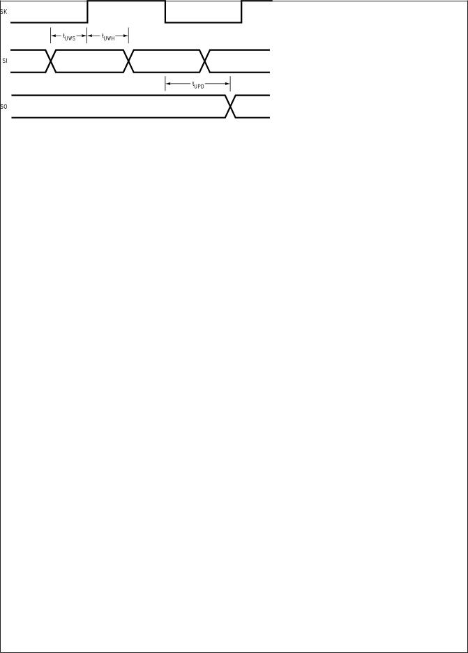
8.0 Electrical Characteristics (Continued)
AC Electrical Characteristics (−40˚C ≤ TA ≤ +125˚C) (Continued)
Note 11: Supply and IDLE currents are measured with CKI driven with a square wave Oscillator, CKO driven 180˚ out of phase with CKI, inputs connected to VCC and outputs driven low but not connected to a load.
Note 12: The HALT mode will stop CKI from oscillating. Measurement of IDD HALT is done with device neither sourcing nor sinking current; with L. A. B, C, E, F, G0, and G2–G5 programmed as low outputs and not driving a load; all D outputs programmed low and not driving a load; all inputs tied to VCC; A/D converter and clock monitor and BOR disabled. Parameter refers to HALT mode entered via setting bit 7 of the G Port data register.
Note 13: Pins G6 and RESET are designed with a high voltage input network. These pins allow input voltages > VCC and the pins will have sink current to VCC when biased at voltages > VCC (the pins do not have source current when biased at a voltage below VCC). These two pins will not latch up. The voltage at the pins must be limited to < (VCC + 7V. WARNING: Voltages in excess of 14V will cause damage to the pins. This warning excludes ESD transients.
Note 14: If timer is in high speed mode, the minimum time is 1 MCLK. If timer is not in high speed mode, the minimum time is 1 tC.
Note 15: Absolute Maximum Ratings should not be exceeded.
Note 16: Vcc must be valid and stable before G6 is raised to a high voltage.
A/D Converter Electrical Characteristics (−40˚C ≤ TA ≤ +125˚C)
(Single-ended mode only)
Datasheet min/max specification limits are guaranteed by design, test, or statistical analysis.
Parameter |
Conditions |
Min |
Typ |
Max |
Units |
|
|
|
|
|
|
Resolution |
|
|
|
10 |
Bits |
|
|
|
|
|
|
DNL |
VCC = 5V |
|
|
±1 |
LSB |
INL |
VCC = 5V |
|
|
±3 |
LSB |
Offset Error |
VCC = 5V |
|
|
+2.5, −1 |
LSB |
Gain Error |
VCC = 5V |
|
|
+0.5, −2.5 |
LSB |
Input Voltage Range |
4.5V ≤ VCC < 5.5V |
0 |
|
VCC |
V |
Analog Input Leakage Current |
|
|
|
0.5 |
µA |
|
|
|
|
|
|
Analog Input Resistance (Note 9) |
|
|
|
6k |
Ω |
Analog Input Capacitance |
|
|
|
7 |
pF |
|
|
|
|
|
|
Conversion Clock Period |
4.5V ≤ VCC < 5.5V |
0.8 |
|
30 |
µs |
Conversion Time (including S/H Time) |
|
|
15 |
|
A/D |
|
|
|
|
|
Conversion |
|
|
|
|
|
Clock |
|
|
|
|
|
Cycles |
|
|
|
|
|
|
Operating Current on AVCC |
AVCC = 5.5V |
|
0.2 |
0.6 |
mA |
Note 17: Resistance between the device input and the internal sample and hold capacitance.
10137405
FIGURE 1. MICROWIRE/PLUS Timing
COP8CBR9/COP8CCR9/COP8CDR9
17 |
www.national.com |
COP8CBR9/COP8CCR9/COP8CDR9
9.0 Pin Descriptions
The COP8CBR/CCR/CDR I/O structure enables designers to reconfigure the microcontroller’s I/O functions with a single instruction. Each individual I/O pin can be independently configured as output pin low, output high, input with high impedance or input with weak pull-up device. A typical example is the use of I/O pins as the keyboard matrix input lines. The input lines can be programmed with internal weak pull-ups so that the input lines read logic high when the keys are all open. With a key closure, the corresponding input line will read a logic zero since the weak pull-up can easily be overdriven. When the key is released, the internal weak pull-up will pull the input line back to logic high. This eliminates the need for external pull-up resistors. The high current options are available for driving LEDs, motors and speakers. This flexibility helps to ensure a cleaner design, with less external components and lower costs. Below is the general description of all available pins.
VCC and GND are the power supply pins. All VCC and GND pins must be connected.
Users of the LLP package are cautioned to be aware that the central metal area and the pin 1 index mark on the bottom of the package may be connected to GND. See figure below:
10137470
FIGURE 2. LLP Package Bottom View
CKI is the clock input. This can be connected (in conjunction with CKO) to an external crystal circuit to form a crystal oscillator. See Oscillator Description section.
RESET is the master reset input. See Reset description section.
AVCC is the Analog Supply for A/D converter. It should be connected to VCC externally. This is also the top of the resistor ladder D/A converter used within the A/D converter.
AGND is the ground pin for the A/D converter. It should be connected to GND externally. This is also the bottom of the resistor ladder D/A converter used within the A/D converter.
The device contains up to six bidirectional 8-bit I/O ports (A, B, C, E, G and L) and one 4-bit I/O port (F), where each individual bit may be independently configured as an input (Schmitt trigger inputs on ports L and G), output or TRISTATE under program control. Three data memory address locations are allocated for each of these I/O ports. Each I/O port has three associated 8-bit memory mapped registers, the CONFIGURATION register, the output DATA register and the Pin input register. (See the memory map for the various addresses associated with the I/O ports.) Figure 3 shows the I/O port configurations. The DATA and CONFIGURATION registers allow for each port bit to be individually configured
under software control as shown below:
CONFIGURATION |
DATA |
Port Set-Up |
|
Register |
Register |
||
|
|||
|
|
|
|
0 |
0 |
Hi-Z Input |
|
|
|
(TRI-STATE Output) |
|
|
|
|
|
0 |
1 |
Input with Weak Pull-Up |
|
|
|
|
|
1 |
0 |
Push-Pull Zero Output |
|
|
|
|
|
1 |
1 |
Push-Pull One Output |
|
|
|
|
Port A is an 8-bit I/O port. All A pins have Schmitt triggers on the inputs. The 44-pin package does not have a full 8-bit port and contains some unbonded, floating pads internally on the chip. The binary value read from these bits is undetermined. The application software should mask out these unknown bits when reading the Port A register, or use only bit-access program instructions when accessing Port A. These unconnected bits draw power only when they are addressed (i.e., in brief spikes). Additionally, if Port A is being used with some combination of digital inputs and analog inputs, the analog inputs will read as undetermined values and should be masked out by software.
Port A supports the analog inputs for the A/D converter. Port A has the following alternate pin functions:
A7 Analog Channel 7
A6 Analog Channel 6
A5 Analog Channel 5
A4 Analog Channel 4
A3 Analog Channel 3
A2 Analog Channel 2
A1 Analog Channel 1
A0 Analog Channel 0
Port B is an 8-bit I/O port. All B pins have Schmitt triggers on the inputs. If Port B is being used with some combination of digital inputs and analog inputs, the analog inputs will read as undetermined values. The application software should mask out these unknown bits when reading the Port B register, or use only bit-access program instructions when accessing Port B.
Port B supports the analog inputs for the A/D converter. Port B has the following alternate pin functions:
B7 Analog Channel 15 or A/D Input
B6 Analog Channel 14 or Analog Multiplexor Output
B5 Analog Channel 13 or Analog Multiplexor Output
B4 Analog Channel 12
B3 Analog Channel 11
B2 Analog Channel 10
B1 Analog Channel 9
B0 Analog Channel 8
Port C is an 8-bit I/O port. The 44-pin device does not offer Port C. The unavailable pins are not terminated. A read operation on these unterminated pins will return unpredictable values. On this device, the associated Port C Data and Configuration registers should not be used. All C pins have Schmitt triggers on the inputs. Port C draws no power when unbonded.
Port E is an 8-bit I/O Port. The 44-pin device does not offer Port E. The unavailable pins are not terminated. A read operation on these unterminated pins will return unpredictable values. On this device, the associated Port E Data and
www.national.com |
18 |

9.0 Pin Descriptions (Continued)
Configuration registers should not be used. All E pins have Schmitt triggers on the inputs. Port E draws no power when unbonded.
Port F is a 4-bit I/O Port. All F pins have Schmitt triggers on the inputs.
The 68-pin package has fewer than eight Port F pins, and contains unbonded, floating pads internally on the chip. The binary values read from these bits are undetermined. The application software should mask out these unknown bits when reading the Port F register, or use only bit-access program instructions when accessing Port F. The unconnected bits draw power only when they are addressed (i.e., in brief spikes).
Port G is an 8-bit port. Pin G0, G2–G5 are bi-directional I/O ports. Pin G6 is always a general purpose Hi-Z input. All pins have Schmitt Triggers on their inputs. Pin G1 serves as the dedicated WATCHDOG output with weak pull-up if the WATCHDOG feature is selected by the Option register. The pin is a general purpose I/O if WATCHDOG feature is not selected. If WATCHDOG feature is selected, bit 1 of the Port G configuration and data register does not have any effect on Pin G1 setup. G7 serves as the dedicated output pin for the CKO clock output.
Since G6 is an input only pin and G7 is the dedicated CKO clock output pin, the associated bits in the data and configuration registers for G6 and G7 are used for special purpose functions as outlined below. Reading the G6 and G7 data bits will return zeros.
The device will be placed in the HALT mode by writing a “1” to bit 7 of the Port G Data Register. Similarly the device will be placed in the IDLE mode by writing a “1” to bit 6 of the Port G Data Register.
Writing a “1” to bit 6 of the Port G Configuration Register enables the MICROWIRE/PLUS to operate with the alternate phase of the SK clock. The G7 configuration bit, if set high, enables the clock start up delay after HALT when the R/C clock configuration is used.
|
|
Config. Reg. |
Data Reg. |
|
|
|
|
|
G7 |
CLKDLY |
HALT |
|
|
|
|
|
G6 |
Alternate SK |
IDLE |
|
|
|
|
Port G has the following alternate features: |
|||
G7 |
CKO Oscillator dedicated output |
|
|
G6 |
SI (MICROWIRE/PLUS Serial Data Input) |
||
G5 |
SK (MICROWIRE/PLUS Serial Clock) |
||
G4 |
SO (MICROWIRE/PLUS Serial Data Output) |
||
G3 |
T1A (Timer T1 I/O) |
|
|
G2 |
T1B (Timer T1 Capture Input) |
|
|
G1 |
WDOUT WATCHDOG and/or Clock Monitor if WATCH- |
||
|
DOG enabled, otherwise it is a general purpose I/O |
||
G0 |
INTR (External Interrupt Input) |
|
|
G0 through G3 are also used for In-System Emulation.
Port L is an 8-bit I/O port. All L-pins have Schmitt triggers on the inputs.
Port L supports the Multi-Input Wake-up feature on all eight pins. Port L has the following alternate pin functions:
L7 Multi-Input Wake-up or T3B (Timer T3B Input)
L6 Multi-Input Wake-up or T3A (Timer T3A Input/Output) L5 Multi-Input Wake-up or T2B (Timer T2B Input)
L4 Multi-input Wake-up or T2A (Timer T2A Input/Output)
L3 Multi-Input Wake-up and/or RDX (USART Receive)
L2 Multi-Input Wake-up or TDX (USART Transmit)
L1 Multi-Input Wake-up and/or CKX (USART Clock) (Low Speed Oscillator Output)
L0 Multi-Input Wake-up (Low Speed Oscillator Input)
Port D is an 8-bit output port that is preset high when RESET goes low. The user can tie two or more D port outputs (except D2) together in order to get a higher drive.
Note: Care must be exercised with the D2 pin operation. At RESET, the external loads on this pin must ensure that the output voltages stay above 0.7 VCC to prevent the chip from entering special modes. Also keep the external loading on D2 to less than 1000 pF.
10137406
FIGURE 3. I/O Port Configurations
10137407
FIGURE 4. I/O Port Configurations — Output Mode
COP8CBR9/COP8CCR9/COP8CDR9
19 |
www.national.com |
COP8CBR9/COP8CCR9/COP8CDR9
9.0 Pin Descriptions (Continued)
10137408
FIGURE 5. I/O Port Configurations — Input Mode
9.1 EMULATION CONNECTION
Connection to the emulation system is made via a 2 x 7 connector which interrupts the continuity of the RESET, G0, G1, G2 and G3 signals between the COP8 device and the rest of the target system (as shown in Figure 6). This connector can be designed into the production pc board and can be replaced by jumpers or signal traces when emulation is no longer necessary. The emulator will replicate all functions of G0 - G3 and RESET. For proper operation, no connection should be made on the device side of the emulator connector.
10137409
FIGURE 6. Emulation Connection
10.0 Functional Description
The architecture of the device is a modified Harvard architecture. With the Harvard architecture, the program memory (Flash) is separate from the data store memory (RAM). Both Program Memory and Data Memory have their own separate
addressing space with separate address buses. The architecture, though based on the Harvard architecture, permits transfer of data from Flash Memory to RAM.
10.1 CPU REGISTERS
The CPU can do an 8-bit addition, subtraction, logical or shift operation in one instruction (tC) cycle time.
There are six CPU registers:
A is the 8-bit Accumulator Register
PC is the 15-bit Program Counter Register
PU is the upper 7 bits of the program counter (PC)
PL is the lower 8 bits of the program counter (PC)
B is an 8-bit RAM address pointer, which can be optionally post auto incremented or decremented.
X is an 8-bit alternate RAM address pointer, which can be optionally post auto incremented or decremented.
S is the 8-bit Data Segment Address Register used to extend the lower half of the address range (00 to 7F) into 256 data segments of 128 bytes each.
SP is the 8-bit stack pointer, which points to the subroutine/ interrupt stack (in RAM). With reset the SP is initialized to RAM address 06F Hex. The SP is decremented as items are pushed onto the stack. SP points to the next available location on the stack.
All the CPU registers are memory mapped with the exception of the Accumulator (A) and the Program Counter (PC).
10.2 PROGRAM MEMORY
The program memory consists of 32,768 bytes of Flash Memory. These bytes may hold program instructions or constant data (data tables for the LAID instruction, jump vectors for the JID instruction, and interrupt vectors for the VIS instruction). The program memory is addressed by the 15-bit program counter (PC). All interrupts in the device vector to program memory location 00FF Hex. The program memory reads 00 Hex in the erased state. Program execution starts at location 0 after RESET.
If a Return instruction is executed when the SP contains 6F (hex), instruction execution will continue from Program Memory location 7FFF (hex). If location 7FFF is accessed by an instruction fetch, the Flash Memory will return a value of 00. This is the opcode for the INTR instruction and will cause a Software Trap.
For the purpose of erasing and rewriting the Flash Memory, it is organized in pages of 128 bytes.
10.3 DATA MEMORY
The data memory address space includes the on-chip RAM and data registers, the I/O registers (Configuration, Data and Pin), the control registers, the MICROWIRE/PLUS SIO shift register, and the various registers, and counters associated with the timers and the USART (with the exception of the IDLE timer). Data memory is addressed directly by the instruction or indirectly by the B, X and SP pointers.
The data memory consists of 1024 bytes of RAM. Sixteen bytes of RAM are mapped as “registers” at addresses 0F0 to 0FF Hex. These registers can be loaded immediately, and also decremented and tested with the DRSZ (decrement register and skip if zero) instruction. The memory pointer registers X, SP, B and S are memory mapped into this space at address locations 0FC to 0FF Hex respectively, with the other registers being available for general usage.
www.national.com |
20 |
10.0 Functional Description
(Continued)
The instruction set permits any bit in memory to be set, reset or tested. All I/O and registers (except A and PC) are memory mapped; therefore, I/O bits and register bits can be directly and individually set, reset and tested. The accumulator (A) bits can also be directly and individually tested.
Note: RAM contents are undefined upon power-up.
10.4 DATA MEMORY SEGMENT RAM EXTENSION
Data memory address 0FF is used as a memory mapped location for the Data Segment Address Register (S).
The data store memory is either addressed directly by a single byte address within the instruction, or indirectly relative to the reference of the B, X, or SP pointers (each contains a single-byte address). This single-byte address allows an addressing range of 256 locations from 00 to FF hex. The upper bit of this single-byte address divides the data store memory into two separate sections as outlined previously. With the exception of the RAM register memory from address locations 00F0 to 00FF, all RAM memory is memory mapped with the upper bit of the single-byte address being equal to zero. This allows the upper bit of the single-byte address to determine whether or not the base address range (from 0000 to 00FF) is extended. If this upper bit equals one (representing address range 0080 to 00FF), then address extension does not take place. Alternatively, if this upper bit equals zero, then the data segment extension register S is used to extend the base address range (from 0000 to 007F) from XX00 to XX7F, where XX represents the 8 bits from the S register. Thus the 128-byte data segment extensions are located from addresses 0100 to 017F for data segment 1, 0200 to 027F for data segment 2, etc., up to FF00 to FF7F for data segment 255. The base address range from 0000 to 007F represents data segment 0.
Figure 7 illustrates how the S register data memory extension is used in extending the lower half of the base address
range (00 to 7F hex) into 256 data segments of 128 bytes each, with a total addressing range of 32 kbytes from XX00 to XX7F. This organization allows a total of 256 data segments of 128 bytes each with an additional upper base segment of 128 bytes. Furthermore, all addressing modes are available for all data segments. The S register must be changed under program control to move from one data segment (128 bytes) to another. However, the upper base segment (containing the 16 memory registers, I/O registers, control registers, etc.) is always available regardless of the contents of the S register, since the upper base segment (address range 0080 to 00FF) is independent of data segment extension.
The instructions that utilize the stack pointer (SP) always reference the stack as part of the base segment (Segment 0), regardless of the contents of the S register. The S register is not changed by these instructions. Consequently, the stack (used with subroutine linkage and interrupts) is always located in the base segment. The stack pointer will be initialized to point at data memory location 006F as a result of reset.
The 128 bytes of RAM contained in the base segment are split between the lower and upper base segments. The first 112 bytes of RAM are resident from address 0000 to 006F in the lower base segment, while the remaining 16 bytes of RAM represent the 16 data memory registers located at addresses 00F0 to 00FF of the upper base segment. No RAM is located at the upper sixteen addresses (0070 to 007F) of the lower base segment.
Additional RAM beyond these initial 128 bytes, however, will always be memory mapped in groups of 128 bytes (or less) at the data segment address extensions (XX00 to XX7F) of the lower base segment. The additional 892 bytes of RAM in this device are memory mapped at address locations 0100 to 017F through 0700 to 077F hex.
COP8CBR9/COP8CCR9/COP8CDR9
21 |
www.national.com |
COP8CBR9/COP8CCR9/COP8CDR9
10.0 Functional Description (Continued)
10137410
FIGURE 7. RAM Organization
10.4.1 Virtual EEPROM
The Flash memory and the User ISP functions (see Section 5.7), provide the user with the capability to use the flash program memory to back up user defined sections of RAM. This effectively provides the user with the same nonvolatile data storage as EEPROM. Management, and even the amount of memory used, are the responsibility of the user, however the flash memory read and write functions have been provided in the boot ROM.
One typical method of using the Virtual EEPROM feature would be for the user to copy the data to RAM during system initialization, periodically, and if necessary, erase the page of Flash and copy the contents of the RAM back to the Flash.
10.5 OPTION REGISTER
The Option register, located at address 0x7FFF in the Flash Program Memory, is used to configure the user selectable security, WATCHDOG, and HALT options. The register can be programmed only in external Flash Memory programming or ISP Programming modes. Therefore, the register must be programmed at the same time as the program memory. The contents of the Option register shipped from the factory read 00 Hex.
www.national.com |
22 |
10.0 Functional Description
(Continued)
The format of the Option register is as follows:
Bit 7 |
Bit 6 |
Bit 5 |
Bit 4 |
Bit 3 |
Bit 2 |
Bit 1 |
Bit 0 |
|
|
|
|
|
|
|
|
|
|
Reserved |
SECURITY |
Reserved |
WATCH |
HALT |
FLEX |
|||
DOG |
||||||||
|
|
|
|
|
|
|
||
|
|
|
|
|
|
|
|
|
Bits 7, 6 These bits are reserved and must be 0.
Bit 5
=1 Security enabled. Flash Memory read and write are not allowed except in User ISP/Virtual E2 commands. Mass Erase is allowed.
=0 Security disabled. Flash Memory read and write are allowed.
Bits 4, 3 These bits are reserved and must be 0.
Bit 2
=1 WATCHDOG feature disabled. G1 is a general purpose I/O.
=0 WATCHDOG feature enabled. G1 pin is WATCHDOG output with weak pullup.
Bit 1
=1 HALT mode disabled.
=0 HALT mode enabled. Bit 0
=1 Execution following RESET will be from Flash Memory.
=0 Flash Memory is erased. Execution following RESET will be from Boot ROM with the MICROWIRE/ PLUS ISP routines.
The COP8 assembler defines a special ROM section type, CONF, into which the Option Register data may be coded. The Option Register is programmed automatically by programmers that are certified by National.
The user needs to ensure that the FLEX bit will be set when the device is programmed.
The following examples illustrate the declaration of the Option Register.
Syntax: |
|
|
[label:].sect |
config, conf |
|
.db |
value |
;1 byte, |
|
|
;configures |
|
|
;options |
.endsect
Example: The following sets a value in the Option Register and User Identification for a COP8CBR9HVA7. The Option Register bit values shown select options: Security disabled, WATCHDOG enabled HALT mode enabled and execution will commence from Flash Memory.
.chip |
8CBR |
|
.sect |
option, conf |
|
.db |
0x01 |
;wd, halt, flex |
.endsect |
|
|
... |
|
|
.end |
start |
|
Note: All programmers certified for programming this family of parts will support programming of the Option Register. Please contact National or your device programmer supplier for more information.
10.6 SECURITY
The device has a security feature which, when enabled, prevents external reading of the Flash program memory. The security bit in the Option Register determines, whether security is enabled or disabled. If the security feature is disabled, the contents of the internal Flash Memory may be read by external programmers or by the built in MICROWIRE/PLUS serial interface ISP. Security must be enforced by the user when the contents of the Flash Memory are accessed via the user ISP or Virtual EEPROM capability.
If the security feature is enabled, then any attempt to externally read the contents of the Flash Memory will result in the value FF (hex) being read from all program locations (except the Option Register). In addition, with the security feature enabled, the write operation to the Flash program memory and Option Register is inhibited. Page Erases are also inhibited when the security feature is enabled. The Option Register is readable regardless of the state of the security bit by accessing location FFFF (hex). Mass Erase Operations are possible regardless of the state of the security bit.
The security bit can be erased only by a Mass Erase of the entire contents of the Flash unless Flash operation is under the control of User ISP functions.
Note: The actual memory address of the Option Register is 7FFF (hex), however the MICROWIRE/PLUS ISP routines require the address FFFF (hex) to be used to read the Option Register when the Flash Memory is secured.
The entire Option Register must be programmed at one time and cannot be rewritten without first erasing the entire last page of Flash Memory.
10.7 RESET
The device is initialized when the RESET pin is pulled low or the On-chip Brownout Reset is activated. The Brownout Reset feature is not available on the COP8CDR9.
10137411
FIGURE 8. Reset Logic
The following occurs upon initialization:
Port A: TRI-STATE (High Impedance Input)
Port B: TRI-STATE (High Impedance Input)
Port C: TRI-STATE (High Impedance Input)
Port D: HIGH
Port E: TRI-STATE (High Impedance Input)
Port F: TRI-STATE (High Impedance Input)
Port G: TRI-STATE (High Impedance Input). Exceptions: If Watchdog is enabled, then G1 is Watchdog output. G0 and G2 have their weak pull-up enabled during RESET.
Port L: TRI-STATE (High Impedance Input)
PC: CLEARED to 0000
PSW, CNTRL and ICNTRL registers: CLEARED
SIOR:
UNAFFECTED after RESET with power already applied
RANDOM after RESET at power-on
COP8CBR9/COP8CCR9/COP8CDR9
23 |
www.national.com |
COP8CBR9/COP8CCR9/COP8CDR9
10.0 Functional Description
(Continued)
T2CNTRL: CLEARED
T3CNTRL: CLEARED
HSTCR: CLEARED
ITMR: Cleared except Bit 6 (HSON) = 1
Accumulator, Timer 1, Timer 2 and Timer 3:
RANDOM after RESET
WKEN, WKEDG: CLEARED
WKPND: RANDOM
SP (Stack Pointer):
Initialized to RAM address 06F Hex
B and X Pointers:
UNAFFECTED after RESET with power already applied
RANDOM after RESET at power-on
S Register: CLEARED
RAM:
UNAFFECTED after RESET with power already applied
RANDOM after RESET at power-on
USART:
PSR, ENU, ENUR, ENUI: Cleared except the TBMT bit
which is set to one.
ANALOG TO DIGITAL CONVERTER:
ENAD: CLEARED
ADRSTH: RANDOM
ADRSTL: RANDOM
ISP CONTROL:
ISPADLO: CLEARED
ISPADHI: CLEARED
PGMTIM: PRESET TO VALUE FOR 10 MHz CKI
WATCHDOG (if enabled):
The device comes out of reset with both the WATCHDOG logic and the Clock Monitor detector armed, with the WATCHDOG service window bits set and the Clock Monitor bit set. The WATCHDOG and Clock Monitor circuits are inhibited during reset. The WATCHDOG service window bits being initialized high default to the maximum WATCHDOG service window of 64k T0 clock cycles. The Clock Monitor bit being initialized high will cause a Clock Monitor error following reset if the clock has not reached the minimum specified frequency at the termination of reset. A Clock Monitor error will cause an active low error output on pin G1. This error output will continue until 16–32 T0 clock cycles following the clock frequency reaching the minimum specified value, at which time the G1 output will go high.
10.7.1 External Reset
The RESET input when pulled low initializes the device. The RESET pin must be held low for a minimum of one instruction cycle to guarantee a valid reset. During Power-Up initialization, the user must ensure that the RESET pin of a device without the Brownout Reset feature is held low until the device is within the specified VCC voltage. Any rising edge on the RESET pin while VCC is below the specified operating range may cause unpredictable results. An R/C circuit on the RESET pin with a delay 5 times (5x) greater than the power supply rise time is recommended. Reset should also be wide enough to ensure crystal start-up upon Power-Up.
RESET may also be used to cause an exit from the HALT mode.
A recommended reset circuit for this device is shown in
Figure 9.
10137412
FIGURE 9. Reset Circuit Using External Reset
10.7.2 On-Chip Brownout Reset
When enabled, the device generates an internal reset as VCC rises. While VCC is less than the specified brownout voltage (Vbor), the device is held in the reset condition and the Idle Timer is preset with 00Fx (240–256 tC). When VCC reaches a value greater than Vbor, the Idle Timer starts counting down. Upon underflow of the Idle Timer, the internal reset is released and the device will start executing instructions. This internal reset will perform the same functions as external reset. Once VCC is above the Vbor and this initial Idle Timer time-out takes place, instruction execution begins and the Idle Timer can be used normally. If, however, VCC drops below the selected Vbor, an internal reset is generated, and the Idle Timer is preset with 00Fx. The device now waits until VCC is greater than Vbor and the countdown starts over. When enabled, the functional operation of the device, at frequency, is guaranteed down to the Vbor level.
www.national.com |
24 |
10.0 Functional Description (Continued)
10137413
FIGURE 10. Brownout Reset Operation
One exception to the above is that the brownout circuit will insert a delay of approximately 3 ms on power up or any time the VCC drops below a voltage of about 1.8V. The device will be held in Reset for the duration of this delay before the Idle Timer starts counting the 240 to 256 tC. This delay starts as soon as the VCC rises above the trigger voltage (approximately 1.8V). This behavior is shown in Figure 10.
In Case 1, VCC rises from 0V and the on-chip RESET is undefined until the supply is greater than approximately 1.0V. At this time the brownout circuit becomes active and holds the device in RESET. As the supply passes a level of about 1.8V, a delay of about 3 ms (td) is started and the Idle Timer is preset to a value between 00F0 and 00FF (hex).
Once VCC is greater than Vbor and td has expired, the Idle Timer is allowed to count down (tid).
Case 2 shows a subsequent dip in the supply voltage which goes below the approximate 1.8V level. As VCC drops below Vbor, the internal RESET signal is asserted. When VCC rises back above the 1.8V level, td is started. Since the power supply rise time is longer for this case, td has expired before VCC rises above Vbor and tid starts immediately when VCC is greater than Vbor.
Case 3 shows a dip in the supply where VCC drops below Vbor, but not below 1.8V. On-chip RESET is asserted when
VCC goes below Vbor and tid starts as soon as the supply goes back above Vbor.
If the Brownout Reset feature is enabled, the internal reset will not be turned off until the Idle Timer underflows. The internal reset will perform the same functions as external reset. The device is guaranteed to operate at the specified frequency down to the specified brownout voltage. After the underflow, the logic is designed such that no additional internal resets occur as long as VCC remains above the brownout voltage.
The device is relatively immune to short duration negativegoing VCC transients (glitches). It is essential that good
filtering of VCC be done to ensure that the brownout feature works correctly. Power supply decoupling is vital even in battery powered systems.
There are two optional brownout voltages. The part numbers for the three versions of this device are:
COP8CBR, Vbor = low voltage range
COP8CCR, Vbor = high voltage range
COP8CDR, BOR is disabled.
Refer to the device specifications for the actual Vbor voltages.
High brownout voltage devices are guaranteed to operate at 10MHz down to the brownout voltage. Low brownout voltage devices are guaranteed to operate at 3.33MHz down to the brownout voltage. Devices are not guaranteed to operate at 10MHz down to the low brownout voltage.
Under no circumstances should the RESET pin be allowed to float. If the on-chip Brownout Reset feature is being used, the RESET pin should be connected directly to VCC. The RESET input may also be connected to an external pull-up resistor or to other external circuitry. Any rising edge on the RESET pin while VCC is below the specified operating range may cause unpredictable results. The output of the brownout reset detector will always preset the Idle Timer to a value between 00F0 and 00FF (240 to 256 tC). At this time, the internal reset will be generated.
If the BOR feature is disabled, then no internal resets are generated and the Idle Timer will power-up with an unknown value. In this case, the external RESET must be used. When BOR is disabled, this on-chip circuitry is disabled and draws no DC current.
The contents of data registers and RAM are unknown following the on-chip reset.
COP8CBR9/COP8CCR9/COP8CDR9
25 |
www.national.com |
COP8CBR9/COP8CCR9/COP8CDR9
10.0 Functional Description
(Continued)
10137414
FIGURE 11. Reset Circuit Using Power-On Reset
10.8 OSCILLATOR CIRCUITS
The device has two crystal oscillators to facilitate low power operation while maintaining throughput when required. Further information on the use of the two oscillators is found in
Section 7.0 Power Saving Features. The low speed oscillator utilizes the L0 and L1 port pins. References in the following text to CKI will also apply to L0 and references to G7/CKO will also apply to L1.
10.8.1 Oscillator
CKI is the clock input while G7/CKO is the clock generator output to the crystal. An on-chip bias resistor connected between CKI and CKO is provided to reduce system part count. The value of the resistor is in the range of 0.5M to 2M (typically 1.0M). Table 2 shows the component values required for various standard crystal values. Resistor R2 is on-chip, for the high speed oscillator, and is shown for reference. Figure 12 shows the crystal oscillator connection diagram. A ceramic resonator of the required frequency may be used in place of a crystal if the accuracy requirements are not quite as strict.
High Speed Oscillator |
Low Speed Oscillator |
10137416
10137415
FIGURE 12. Crystal Oscillator
TABLE 2. Crystal Oscillator Configuration,
TA = 25˚C, VCC = 5V
R1 (kΩ) |
R2 (MΩ) |
C1 (pF) |
C2 (pF) |
CKI Freq. |
|
(MHz) |
|||||
|
|
|
|
||
|
|
|
|
|
|
0 |
On Chip |
18 |
18 |
10 |
|
|
|
|
|
|
|
0 |
On Chip |
18 |
18 |
5 |
|
|
|
|
|
|
|
0 |
On Chip |
18–36 |
18–36 |
1 |
|
|
|
|
|
|
|
5.6 |
On Chip |
100 |
100–156 |
0.455 |
|
|
|
|
|
|
|
0 |
20 |
** |
** |
32.768 |
|
|
|
|
|
kHz* |
|
|
|
|
|
|
*Applies to connection to low speed oscillator on port pins L0 and L1 only. **See Note below.
The crystal and other oscillator components should be placed in close proximity to the CKI and CKO pins to minimize printed circuit trace length.
The values for the external capacitors should be chosen to obtain the manufacturer’s specified load capacitance for the crystal when combined with the parasitic capacitance of the trace, socket, and package (which can vary from 0 to 8 pF). The guideline in choosing these capacitors is:
Manufacturer’s specified load cap = (C1 * C2) / (C1 + C2) +
Cparasitic
C2 can be trimmed to obtain the desired frequency. C2 should be less than or equal to C1.
Note: The low power design of the low speed oscillator makes it extremely sensitive to board layout and load capacitance. The user should place the crystal and load capacitors within 1cm. of the device and must ensure that the above equation for load capacitance is strictly followed. If these conditions are not met, the application may have problems with startup of the low speed oscillator.
TABLE 3. Startup Times
CKI Frequency |
Startup Time |
|
|
10 MHz |
1–10 ms |
|
|
3.33 MHz |
3–10 ms |
|
|
1 MHz |
3–20 ms |
|
|
455 kHz |
10–30 ms |
|
|
32 kHz (low speed oscillator) |
2–5 sec |
|
|
www.national.com |
26 |
 Loading...