NSC CLC501MDC, CLC501AWG-MLS, CLC501AMC, CLC501AJP, CLC501AJE-TR13 Datasheet
...
N June 1999
CLC501
High-Speed Output Clamping Op Amp
General Description
The CLC501 is available in several versions to meet a variety of requirements. A three-letter suffix determines the version:
CLC501AJP |
-40°C to +85°C |
8-pin plastic DIP |
CLC501AJE |
-40°C to +85°C |
8-pin plastic SOIC |
DESC SMD number: 5962-89974 |
|
|
Features
■Output clamping (Vhigh and Vlow)
■1ns recovery from clamping/overdrive
■0.05% settling in 12ns
■Characterized and guaranteed at Av = +32
■Low power, 180mW
Applications
■Residue amplifier in high-accuracy, subranging A/D systems
■High-speed communications
■Output clamping applications
■Pulse amplitude modulation systems
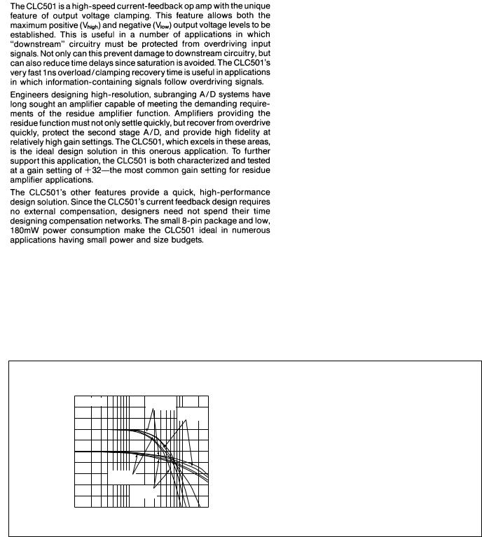
Non-Inverting Frequency Response
|
Vout = 2Vpp |
Rf |
Av = 16 |
|
|
|
= 2.49kΩ |
Av = 8 |
|
|
|
|
|
|
|
|
|
|
Rf = 4.02kΩ |
(1dB/div) |
|
|
|
(deg)Phase |
Magnitude |
|
|
|
0 |
|
|
|
-90 |
|
|
Av = 32 |
|
-180 |
|
|
Rf = 1.5kΩ |
|
-270 |
|
|
|
Av = 64 |
||
|
|
|
||
|
|
Rf = 604Ω |
-360 |
|
|
|
|
|
-450 |
1 |
|
10 |
|
100 |
Pinout
DIP & SOIC
Speed-High |
CLC501 |
Amp Op Clamping Output |
|
© 1999 National Semiconductor Corporation |
http://www.national.com |
Printed in the U.S.A.

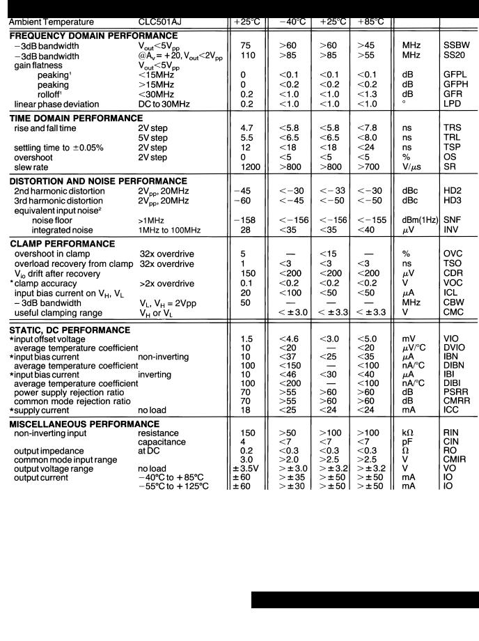
CLC501 Electrical Characteristics (Av = +32,Vcc = ±5V, R L = 100Ω, Rf = 1.5Ω,VH = +3V; unless specified)
Min/max ratings are based on product characterization and simulation. Individual parameters are tested as noted. Outgoing quality levels are determined from tested parameters.
Absolute Maximum Ratings |
Miscellaneous Ratings |
Package Thermal Resistance
|
|
|
Package |
θJC |
θJA |
|
|
|
|
AJP |
70°C/W |
125°C/W |
|
|
|
|
AJE |
65°C/W |
145°C/W |
|
ESD rating (human body model) |
<1000V |
|||||
|
CERDIP |
45°C/W |
135°C/W |
|||
|
|
|
||||
|
|
http://www.national.com |
2 |
 Loading...