


CLC505MDS
NSC CLC505MDS, CLC505MDC, CLC505AMC, CLC505AJP, CLC505AJE-TR13 Datasheet
...
Features
■
10mW power consumption
with 50MHz BW
■
Single-resistor programming of
supply current
■
3.4mA I
cc
provides 100MHz bandwidth
and 14ns settling (0.05%)
■
Fast disable capability
■
0.04% differential gain at I
cc
= 3.4mA
■
0.06% differential phase at I
cc
= 3.4mA
Applications
■
Low-power/battery applications
■
Remote site instrumentation
■
Mobile communications gear
■
Video switching matrix
■
Phased-array radar
General Description
CLC505
High-Speed, Programmable-Supply Current,
Monolithic Op Amp
N
June 1999
CLC505
High-Speed, Programmable-Supply Current, Momolithic Op Amp
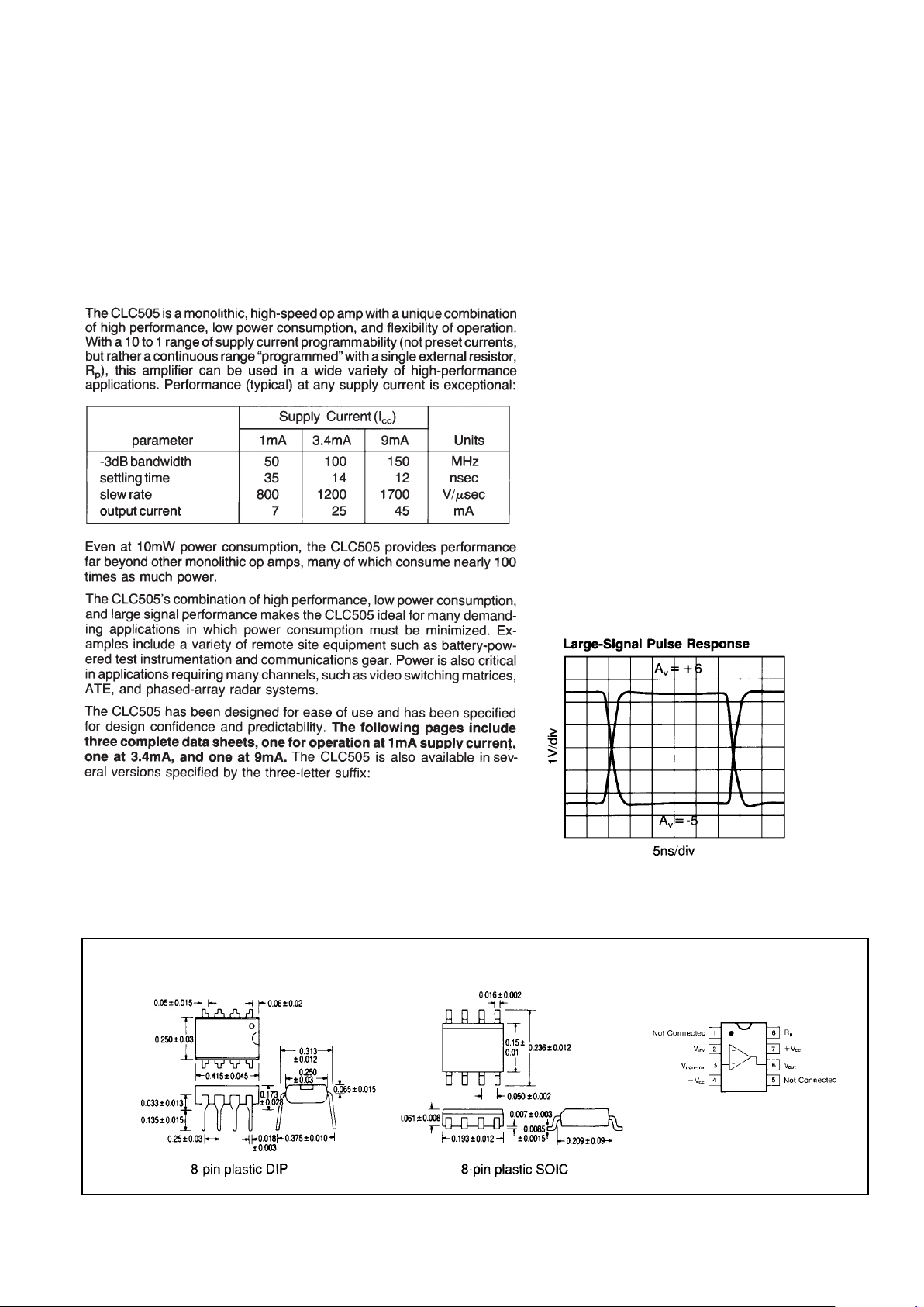
Package Dimensions
Pinout
DIP & SOIC
© 1999 National Semiconductor Corporation http://www.national.com
Printed in the U.S.A.
CLC505AJE -40°C to +85°C 8-pin plastic SOIC
CLC505ALC -40°C to +85°C dice
Contact factory for other packages and DESC SMD number.
http://www.national.com 2
CLC505 Electrical Characteristics
(A
v
= +6,V
cc
= ±5V,R
f
= 1000Ω,C
p
= 100pF;unless specified)
Absolute Maximum Ratings Miscellaneous Ratings
http://www.national.com 2
Min/max ratings are based on product characterization and simulation. Individual parameters are tested as noted. Outgoing quality levels are
determined from tested parameters.
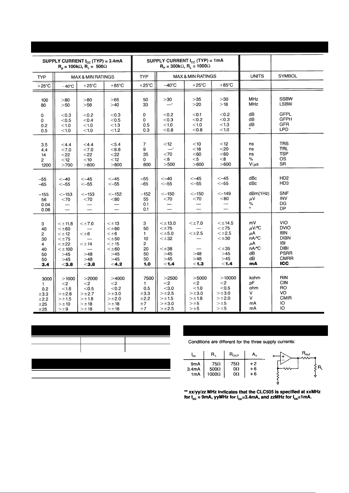
3 http://www.national.com
CLC505 Electrical Characteristics
(A
v
= +6,V
cc
= ±5V,R
f
= 1000Ω,C
p
= 100pF;unless specified)
Notes
<±10.0
<±7.0
<±8.0
Pac kage Thermal Resistance
Package
θθ
JC
θθ
JA
AJE 60°C/W 140°C/W
Reliability Information
Transistor Count 30
http://www.national.com 4
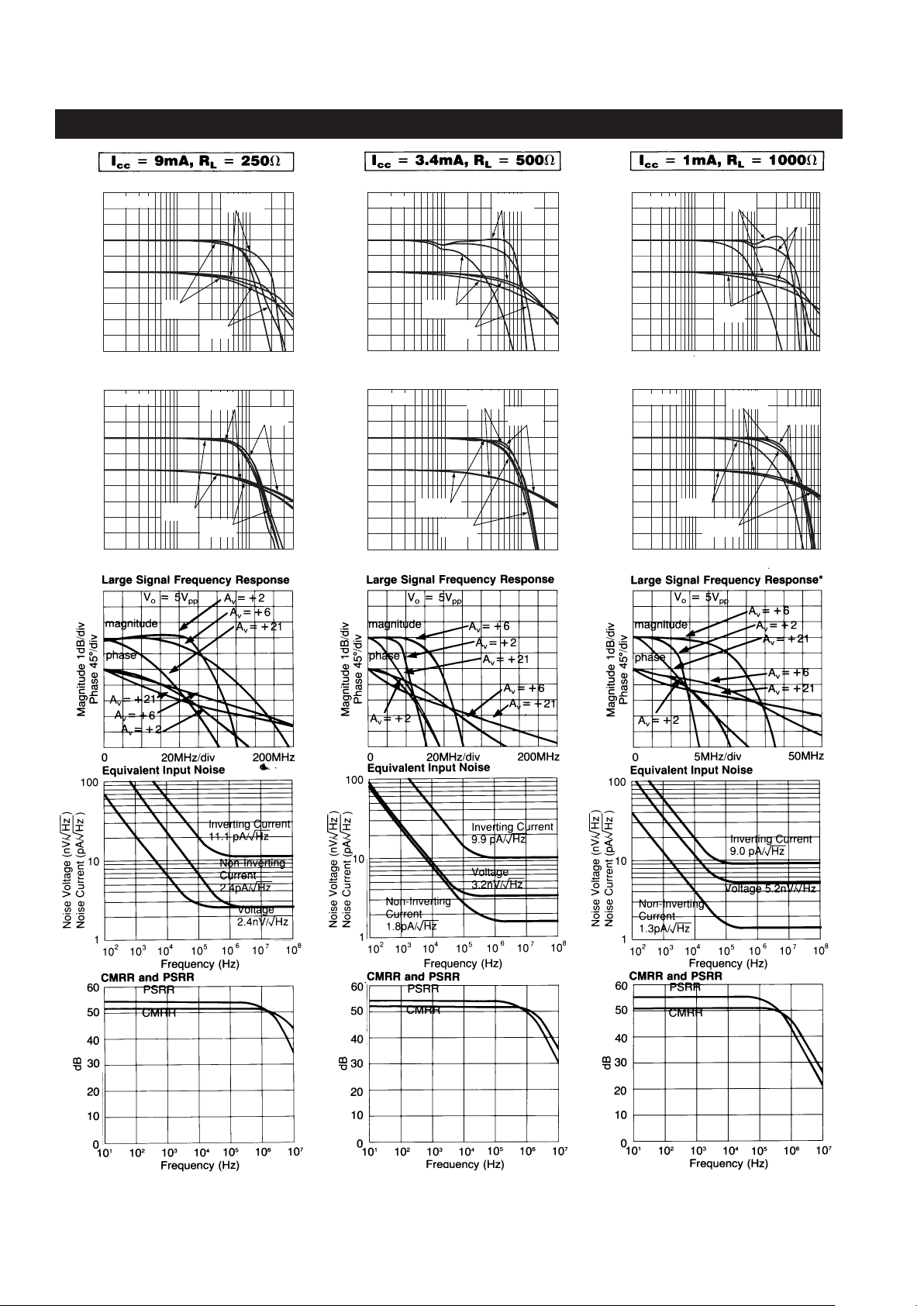
Typical Performance Characteristics
(T
A
= 25°, A
v
= +6,V
CC
= ±5V, R
f
= 1000
ΩΩ
,V
H
= +3V, C
p
= 100pF)
Non-Inverting Frequency Response
Magnitude (1dB/div)
0.1
10
100
Phase (deg)
-180
-450
-270
-360
-90
0
1
V
out
= 2V
pp
A
v
= 2
R
f
= 1kΩ
A
v
= 6
R
f
= 1kΩ
A
v
= 20
R
f
= 1kΩ
Frequency (MHz)
Inverting Frequency Response
Magnitude (1dB/div)
10
100
Phase (deg)
-360
-630
-450
-540
-270
-180
1
V
out
= 2V
pp
A
v
= -2
R
f
= 1.1kΩ
A
v
= -1
R
f
= 1.1kΩ
A
v
= -20
R
f
= 787Ω
A
v
= -6
R
f
= 866Ω
Frequency (MHz)
Inverting Frequency Response
Magnitude (1dB/div)
10
100
Phase (deg)
-360
-630
-450
-540
-270
-180
1
V
out
= 2V
pp
A
v
= -6
R
f
= 866Ω
A
v
= -20
R
f
= 549Ω
A
v
= -1
R
f
= 1.651kΩ
A
v
= -2
R
f
= 1.5kΩ
Frequency (MHz)
Inverting Frequency Response
Magnitude (1dB/div)
0
10
100
Phase (deg)
-360
-630
-450
-540
-270
-180
V
out
= 2V
pp
A
v
= -2
R
f
= 2.87kΩ
A
v
= -1
R
f
= 3.48kΩ
A
v
= -20
R
f
= 1kΩ
A
v
= -6
R
f
= 1.43kΩ
1
Frequency (MHz)
Non-Inverting Frequency Response
Magnitude (1dB/div)
1
10
100
Phase (deg)
-180
-450
-270
-360
-90
0
V
out
= 2V
pp
A
v
= 2
R
f
= 3.01kΩ
A
v
= 20
R
f
= 249Ω
A
v
= 6
R
f
= 1kΩ
Non-Inverting Frequency Response
Magnitude (1dB/div)
1
10
100
Phase (deg)
-180
-450
-270
-360
-90
0
V
out
= 2V
pp
A
v
= 2
R
f
= 3.01kΩ
A
v
= 20
R
f
= 500Ω
A
v
= 6
R
f
= 1kΩ
Frequency (MHz)
Frequency (MHz)
 Loading...